EP0520788A2 - Mémoires à semi-conducteur - Google Patents
Mémoires à semi-conducteur Download PDFInfo
- Publication number
- EP0520788A2 EP0520788A2 EP92305849A EP92305849A EP0520788A2 EP 0520788 A2 EP0520788 A2 EP 0520788A2 EP 92305849 A EP92305849 A EP 92305849A EP 92305849 A EP92305849 A EP 92305849A EP 0520788 A2 EP0520788 A2 EP 0520788A2
- Authority
- EP
- European Patent Office
- Prior art keywords
- writing
- reading
- data latch
- semiconductor memory
- ports
- Prior art date
- Legal status (The legal status is an assumption and is not a legal conclusion. Google has not performed a legal analysis and makes no representation as to the accuracy of the status listed.)
- Withdrawn
Links
Images



Classifications
-
- G—PHYSICS
- G11—INFORMATION STORAGE
- G11C—STATIC STORES
- G11C11/00—Digital stores characterised by the use of particular electric or magnetic storage elements; Storage elements therefor
- G11C11/21—Digital stores characterised by the use of particular electric or magnetic storage elements; Storage elements therefor using electric elements
- G11C11/34—Digital stores characterised by the use of particular electric or magnetic storage elements; Storage elements therefor using electric elements using semiconductor devices
- G11C11/40—Digital stores characterised by the use of particular electric or magnetic storage elements; Storage elements therefor using electric elements using semiconductor devices using transistors
-
- G—PHYSICS
- G11—INFORMATION STORAGE
- G11C—STATIC STORES
- G11C8/00—Arrangements for selecting an address in a digital store
- G11C8/16—Multiple access memory array, e.g. addressing one storage element via at least two independent addressing line groups
Definitions
- the present invention relates to semiconductor memory devices and, more particularly, to semiconductor memory devices having a plurality of writing ports and reading ports.
- microprocessors (arithmetic processing devices, or processors) generally comprise an instruction fetching unit, instruction decoding unit, arithmetic operation executing unit, register file, and the like. Further, these microprocessors have been, for example, designed to execute instructions by pipeline operation.
- a previously-considered microprocessor includes only one arithmetic operation executing unit, and thus the register file may comprise a semiconductor memory device (for example, SRAM) having two-read/one-write ports.
- SRAM semiconductor memory device
- Such semiconductor memory devices having two-read/one-write ports can effectively carry out three address type arithmetic operations, such as adding instructions.
- microprocessors employ parallel processing architecture, such as VLIW (Very Long Instruction Word) or Superscaler, and the like, to enable higher speed processing.
- Microprocessors employing such types of architecture may include a plurality of arithmetic operation executing units and semiconductor memory devices having a plurality of read/write ports for performing a transfer of data between a plurality of arithmetic operation executing units and semiconductor memory devices (register file).
- Such an architecture requires a large number of local register files since it assigns a specific local register file for each sub-routine.
- Such type of register file may, for example, be formed by employing a plurality of two-read/one-write ports semiconductor memory devices.
- An embodiment of the present invention can provide a semiconductor memory device having a plurality of writing ports and reading ports for carrying out parallel writing and reading operations through the writing ports and the reading ports, wherein the semiconductor memory device comprises: a first data latch portion directly accessible by externally entering an address signal; at least one second data latch portions parallel connecting to the first data latch portion; and a communication unit for accessing one of the first-and second data latch portions.
- the writing ports may be operatively connected to the first and second data latch portions through writing control transfer gates, and the reading ports may be operatively connected to the first and second data latch portions through reading control transfer gates.
- the communication unit may comprise a plurality of data latch portion selecting transfer gates provided at a respective writing side and reading side relative to the first and second data latch portions parallel connected, for selecting one of the first and second data latch portions in accordance with a selection signal.
- the selection signal may be dependently generated by using a selection register, or it may be generated by using a selection signal decoder receiving a part of the address signal.
- the writing data may be transferred from the writing ports to one of the first and second data latch portions through a plurality of bit lines for writing, and reading data may be transferred from one of the first and second data latch portions to reading ports through a plurality of bit lines for reading.
- the connection between the bit lines for writing and the first and second data latch portions may be controlled by a plurality of writing port selection gates, and the connection between the first and second data latch portions and the bit lines for reading may be controlled by a plurality of reading port selection gates.
- the writing ports may be operatively connected to the first data latch portion through writing control transfer gates, and the reading ports may be operatively connected to the first data latch portion through reading control transfer gates.
- the communication unit may comprise a plurality of shifting control transfer gates for shifting data of one of the second data latch portions to the first data latch portion and for accessing one of the first and second data latch portions in accordance with a control signal.
- the control signal may be determined to an externally supplied clock signal.
- the writing data may be written from the writing ports into the first data latch portion through a plurality of bit lines for writing, reading data may be read out from the first latch portion to reading ports through a plurality of bit lines for reading, and the data stored in the first data latch portion may be shifted to the second data latch portions.
- the connection between the bit lines for writing and the first data latch portions may be controlled by a plurality of writing port selection gates, and the connection between the first data latch portions and the bit lines for reading may be controlled by a plurality of reading port selection gates.
- a further embodiment of the present invention can provide an arithmetic processing device formed by one chip configuration having an instruction fetching unit for fetching an instruction, an instruction decoding unit for decoding the instruction fetched in the instruction fetching unit, a plurality of arithmetic operation executing units for carrying out arithmetic operations in parallel, and a register file for storing data having a plurality of writing ports and reading ports to carry out writing and reading operations in parallel through the writing ports and the reading ports, wherein the register file comprises: a first data latch portion directly accessible by externally entering an address signal; at least one second data latch portions parallel connecting to the first data latch portion; and a communication unit for accessing one of the first and second data latch portions.
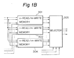
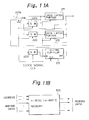
- Figures 1A and 1B show a semiconductor memory device which has a plurality of read/write ports (n-read/m-write ports) and is provided with m write selection switch units (writing port selection gates) 321 to 32m, and n read selection switch units (reading port selection gates) 331 to 33n for one data latch portion (memory cell) 311.
- each of the writing port selection gates 321 to 32m is provided at an intersectional portion between one of the bit lines for writing (writing bit lines) and one of the word lines for writing (writing word lines).
- each of the reading port selection gates 331 to 33n is provided at an intersectional portion between one of the bit lines for reading (reading bit lines) and one of the word lines for reading (reading word lines). Therefore, the number of writing bit lines and writing word lines is the same as the number (m) of writing port selection gates 321 to 32m, and the number of reading bit lines and reading word lines is the same as the number (n) of reading port selection gates 331 to 33n.
- the register file has k memory devices (n-read/m-write memories) 301 to 30k and is designed to be selected by a selector 305.
- the register file of a microprocessor (arithmetic processing devices, or processors) employing parallel processing architecture and local register type (number of local register is generally referred to as k) may be consitituted by k sets of n-read/m-write memories having m writing ports and n reading ports.
- Figure 2 shows a part of a SRAM having four-read/two-write ports to which the semiconductor memory device of Figs. 1A and 1B is applied.
- references BL0 and BL1 denote bit lines for writing (writing bit lines)
- WL0 and WL1 denote word lines for writing (writing word lines)
- BL2, to BL5 denote bit lines for reading (reading bit lines)
- WL2 to WL5 denote word lines for reading (reading word lines).
- the SRAM having four-read/two-write ports has the construction in which two writing port selection gates 321 and 322 and four reading port selection gates 331 to 334 are provided for each SRAM cell 311. Further, each of the writing port selection gates 321 and 322 is provided at an intersectional portion between one of the writing bit lines BL0 and BL1 and one of the writing word lines WL0 and WL1. Similarly, each of the reading port selection gates 331 to 334 is provided at an intersectional portion between one of the reading bit lines BL2 to BL5 and one of the reading word lines WL2 to WL5.
- the two writing ports (WP0, WP1) are operatively connected to the writing bit lines BL0 and BL1 through a sense amplifier, and the like, to write data into each of the SRAM cells 311.
- the four reading ports (RP0, RP1, RP2, RP3) are operatively connected to the reading bit lines BL2 to BL5 through the sense amplifier, and the like, to read out data from each of the SRAM cells 311.
- the writing ports WP0, WP1 and reading ports RP0 to RP3 are not external ports of the microprocessor, but are connected internally of the microprocessor to arithmetic operation executing units (for example, ALUs: Arithmetic and Logic Units) provided in the microprocessor to internally transfer data between the arithmetic operation executing units and the semiconductor memory device (register file).
- arithmetic operation executing units for example, ALUs: Arithmetic and Logic Units
- a semiconductor memory device having a plurality of read/write ports as illustrated in Fig. 1A and-1B is constituted of k local registers (n-read/m-write memories) having m writing ports and n reading ports and thus requires a hardware amount of ((n-read/m-write memories) ⁇ k + selector). Accordingly, multi-port semiconductor memory devices, and microprocessors including such devices, are indesirably expensive.
- two writing ports WP0, WP1 (writing bit lines BL0, BL1) are connected to the SRAM cell 311 (one memory cell) through two writing port selection gates 321 and 322, and four reading ports RP0 to RP3 (reading bit lines BL2 to BL5) are connected to the SRAM cell 311 through four reading port selection gates 331 to 334.
- six transistors (transfer gates 321, 322; 331, 332, 333, 334) are needed for one memory cell (SRAM cell 311). Consequently, the hardware amount required for a large number of memory cells (311) becomes substantial.
- the semiconductor memory device of Fig. 3 has a plurality of read/write ports (n-read/m-write) and comprises m write selection switch units (writing port selection gates) 21 to 2m and n read selection switch units (reading port selection gates) 31 to 3n for a plurality of (k) data latch portions (memory cells) 11 to 1k.
- the semiconductor memory device has a first data latch portion 11 directly accessible by externally entering the address, and second data latch portions 12 to 1k provided parallel to the first data latch portion 11.
- the first and each of the second data latch portions 11 to 1k are provided with respective switching units (data latch portion selecting transfer gates) 41 to 4k and a selector 5.
- switching units 41 to 4k and the selector 5 For each of the switching units 41 to 4k and the selector 5, a selection signal SS is supplied to selectively access one of the first and second data latch portions 11 to 1k.
- the content of the directly accessible memory cell by externally entering an address can be replaced depending upon the designation of the local register file. Namely, by assigning the local register file for respective data latch portions 11 to 1k, one of the targeted data latch portions can be exclusively selected by the switching units 41 to 4k according to the progress of the program.
- Figure 4 shows a part of a SRAM having four-read/two-write ports, to which the semiconductor memory device of Fig. 3 is applied, and further, Fig. 5 shows the configuration of four SRAM cells of Fig. 4.
- references BL0 and BL1 denote bit lines for writing (writing bit lines)
- WL0 and WL1 denote word lines for writing (writing word lines)
- BL2 to BL5 denote bit lines for reading (reading bit lines)
- WL2 to WL5 denote word lines for reading (reading word lines).
- the SRAM has two writing port selection gates 21, 22 and four reading port selection gates 31 to 34 for four SRAM cells 11 to 14. Namely, as shown in Fig. 4, each of the writing port selection gates 21 and 22 is provided at an intersectional portion between one of the writing bit lines BL0 and BL1 and one of the writing word lines WL0 and WL1. Similarly, each of the reading port selection gates 31 to 34 is provided at an intersectional portion between one of the reading bit lines BL2 to BL5 and one of the reading word lines WL2 to WL5. Further, each SRAM 11 to 14 is provided with data latch portion selecting transfer gates 41 to 44 at the writing side and data latch portion selecting transfer gates 51 to 54 at the reading side. These data latch portion selecting transfer gates 41 to 44 and 51 to 54 are controlled by the selection signal SS, so that one of the desired SRAM cells can be selected.
- the two writing ports (WP0, WP1) are operatively connected to the writing bit lines BL0 and BL1 through a sense amplifier, and the like, to write data into one of the selected SRAM cells 11 to 14.
- the four reading ports (RP0, RP1, RP2, RP3) are operatively connected to the reading bit lines BL2, to BL5 through the sense amplifier, and the like, to read out data from one of the selected SRAM cells 11 to 14.
- the writing ports WP0, WP1 and reading ports RP0, to RP3 are not external ports of the microprocessor, but are connected to arithmetic operation execution units (for example, ALUs: Arithmetic and Logic Units) provided in the microprocessor to internally transfer data between the arithmetic operation execution units and the semiconductor memory device (register file).
- arithmetic operation execution units for example, ALUs: Arithmetic and Logic Units
- the present embodiment of a SRAM having four-read/two-write ports of Fig. 4 requires fourteen transistors (transfer gates 21, 22; 31, 32, 33, 34; 41, 42, 43, 44; 51, 52, 53, 54) for four memory cells (SRAM cells) 11, 12, 13 14, however, the SRAM having four-read/two-write ports of Fig. 2 requires six transistors (transfer gates 321, 322; 331, 332, 333, 334) for one memory cell (SRAM cell) 311. Namely, in the present embodiment shown in Fig. 4, only 3.5 (14/4) transistors are required per memory cell, and thus can reduce the hardware amount involved in an SRAM having the same capacity.
- Figure 6 shows a complete semiconductor memory device embodying the present invention.
- reference numeral 100 denotes a selection register
- 200 denotes a row address decoder
- 300 denotes a column address decoder and sense amplifier.
- an address signal (address signals) is supplied to the row address decoder 200 and the column address decoder and sense amplifier 300.
- the two writing ports WP0, WP1 are connected to the memory cells (data latch portions) through sense amplifiers, the writing bit lines BL0 and BL1, and the like.
- the four reading ports RP0, RP1, RP2, RP3 are connected to the memory cells through the sense amplifiers, the reading bit lines BL2 to BL5, and the like.
- the selection register 100 receives selection data and stores the selection data into a register provided in the selection register 100, and further the selection register 100 outputs a selection signal SS to a memory cell array. Namely, the selection signal SS is supplied to the data latch portion selecting transfer gates (41 to 4k and 51 to 54) to selectively access one of the desired first and second data latch portions (11 to 1k.)
- Figure 7 shows an example of a selection signal generation circuit.
- reference numerals 621 to 624 denote selectors
- 631 to 634 denote registers
- 61 denotes an AND gate.
- a shift enabling signal SE is supplied to one input terminal of the AND gate 61 and a clock signal CLK is inverted and supplied to another input terminal of the AND gate 61, and an output signal of the AND gate 61 is supplied to the registers 631 to 634.
- a shift control signal SCS is supplied to the selectors 621 to 624, an output signal of each of the selectors 621 to 624 is supplied to the corresponding registers 631 to 634, and an output signal of each of the registers 631, 632, 633, 634 is supplied to the adjacent selectors 622, 623, 624, 621.
- the selector 621 is constituted by two AND gates 6211 and 6212 and an OR gate 6213.
- the output signal (Q-output signal) of the register 632 is input to one input terminal (S1) of the AND gate 6211, and the shift control signal SCS is inverted and input to another input terminal of the AND gate 6211.
- the output signal (Q-output signal) of the register 634 is input to one input terminal (S2) of the AND gate 6212, and the shift control signal SCS is directly input to another input terminal of the AND gate 6212.
- output signals of the AND gates 6211 and 6212 are input to input terminals of the OR gate 6213.
- each of the selectors 622 to 624 is constituted similarly to the selector 621.
- this selection signal generation circuit of Fig. 7 is used to generate four selection signals SS (SS1 to SS4) for selecting the data latch portion selecting transfer gates 41 to 44 and 51 to 54 shown in Figs. 4 and 5.
- a first selection signal SS is supplied to the gates of the transistors (data latch portion selecting transfer gates) 41 and 51 for a first SRAM cell (memory cell) 11
- a second selection signal SS is supplied to the gates of the transistors 42 and 52 for a second SRAM cell 12
- a third selection signal SS is supplied to the gates of the transistors 43 and 53 for a third SRAM cell 13
- a fourth selection signal SS4 is supplied to the gates of the transistors 44 and 54 for a fourth SRAM cell 14.
- the shift enabling signal SE when the shift enabling signal SE is at a high level "H”, the selection signals SS1 to SS4 are shifted, that is the selection signals SS1 to SS4 are output in a sequential fashion. Namely, the SRAM cells 11 to 14 are selected sequentially and accessed. Conversely, when the shift-enabling signal SE is at a low level "L”, the selection signals SS, to SS4 are not shifted.
- the shift enabling signal SE is at the high level "H”
- the shift control signal SCS is at a high level "H”
- the selection signals SS1 to SS4 are shifted in clockwise rotation, so that the four SRAM cells 11 to 14 are accessed in an orderly manner.
- the SRAM cells 11 to 14 of Fig. 4 are selected as 11 ⁇ 12 ⁇ 13 ⁇ 14 ⁇ 11 ⁇ ⁇ , in accordance with the clock signal CLK.
- the shift enabling signal SE is at the high level "H”
- the shift control signal SCS is at a low level "L”
- the SRAM cells 11 to 14 of Fig. 4 are selected as 11 ⁇ 14 ⁇ 13 ⁇ 12 ⁇ 11 ⁇ ⁇ , in accordance with the clock signal CLK.
- FIG. 8 is a block diagram showing another example of a selection signal generation circuit.
- a reference numeral 400 denotes a selection signal decoder.
- the selection signal generation circuit shown in Fig. 8 generates the selection signal SS by using address signals (AD0 and AD1); however, the selection signal generation circuit shown in Fig. 7 generates the selection signal SS by using the shift enabling signal SE, the shift control signal SCS, and the clock signal CLK.
- j-bits of the address signals AD0 to ADj supplied to the semiconductor memory device consist of two components AD0, AD1 and AD2 to ADj.
- One component the address signals AD0 and AD1) is used to generate the selection signal SS (for example, four selection signals SS1 to SS4), and the other component of the address signals (AD2 to ADj), which corresponds to normal address signals, is used to select and access a specific memory cell in the memory cell array.
- the selection signal SS for example, four selection signals SS1 to SS4
- AD2 to ADj which corresponds to normal address signals
- FIG. 9 is a block diagram showing an example of a microprocessor employing two arithmetic operation execution units and a semiconductor memory device embodying the present invention.
- reference numeral 1 denotes a register file (semiconductor memory device); 2 and 3 denote ALUs (arithmetic operation execution units); 100 denotes a selection register, 101 denotes an instruction decoding unit, and 102 denotes an instruction fetching unit.
- ALUs 2 and 1 are provided, and thus the register file 1 is constituted of a four-read/two-write memory (SRAM having four-read/two-write ports).
- the microprocessor (arithmetic processing device), which is formed by one chip configuration, comprises the instruction fetching unit 102, the instruction decoding unit 101, the register file 1, and two ALUs 2, 3.
- the instruction fetching unit 102 is used to fetch an instruction
- the instruction decoding unit 101 is used to decode the instruction fetched in the instruction fetching unit 102.
- the register file 1 is used to store data
- the ALUs are used to carry out parallel arithmetic operations.
- the register file (semiconductor memory device) 1 includes a plurality of data latch portions 11 to 14, and selectors 51 to 54 (corresponding to selector 5).
- the ALU 2 is connected to the register file 1 by one writing port WP0 (writing bit line BL0) and two reading ports RP0 and RP1 (reading bit lines BL2 and BL3), and similarly, the ALU 3 is connected to the register file 1 by one writing port WP1 (writing bit line BL1) and two reading ports RP2 and RP3 (reading bit lines BL4 and BL5).
- WP0 writing bit line BL0
- RP1 reading bit line BL1
- RP2 and RP3 reading bit lines BL4 and BL5
- Figure 10 shows another semiconductor memory device embodying the present invention.
- a plurality of data latch portions 11 to 1k are parallel connected and one of the data latch portions 11 to 1k is randomly selected by the selection signal SS.
- a first data latch portion Ill directly accessible by externally entering an address
- a plurality of second data latch portions 112 to 11k provided in parallel formation relative to the first data latch portion 11L are directly connected by a communication unit (not shown) so that one of the first and second data latch portion 111 to 11k can be accessed by shifting the data in order (for example, clockwise shifting) with a clock signal CLK.
- the data stored in the data latch portion 113 when data stored in the data latch portion 113 are read out, the data stored in the data latch portion 113 is shifted to the data latch portion 111 through the data latch portion 112 with two cycles of a clock signal CLK, and then the data shifted to the data latch portion 111 is read out.
- the data when writing specific data into the data latch portion 113 after writing the specific data at the data latch portion 111, the data is shifted to the data latch portion 113 in order by the clock signal CLK.
- the second data latch portions (112 to 11k) may be determined to one.
- the data shift of the clockwise rotation denotes that data stored (latched) in the first SRAM cell 111 is transferred to the second SRAM cell 112, or data stored in the third SRAM cell 113 is transferred to the fourth SRAM cell 114 in response to one clock signal CLK.
- Figures 11A and 11B show a practical embodiment of the semiconductor memory device of Fig. 10.
- each of the switching units 221a, 221b, 222 and 223 is, for example, constituted by an N-type MOS transistor, and each of the data latch portions 211, 212 and 213 is, for example, constituted by a D-type flip-flop.
- each data latch portion 211, 212 and 213 are adapted to be both clockwise and counterclockwise shifted.
- three bit memory cells (data latch portion) are provided, but it will be appreciated that memory cells having k bits may be provided to shift the data, as required.
- the signal to control the shifting of data need not be the clock signal CLK supplied from an external semiconductor memory device
- the register file is formed with only a n-read/m-write ⁇ k memory 500 having k number of memory cells.
- a semiconductor memory device (n-read/m-write memory 301 to 30k) having the same capacity as that of Figs. 1A and 1B can be constituted of only the n-read/m-write ⁇ k memory 500, so that the hardware amount can be significantly reduced.
- the semiconductor memory device can be separated into a memory cell array portion and a peripheral portion (decoder, buffer, selector, sense amplifier, and the like).
- the amount of hardware of the register file of the microprocessor employing a parallel processing and local register architecture can be reduced.
- the hardware amount can be reduced significantly.
- the hardware amount of the register file of a microprocessor employing parallel processing and local register architecture can be significantly reduced by providing a first data latch portion and at least one second data latch portion having a communication unit and accessing one of the desired first and second data latch portions.
Landscapes
- Engineering & Computer Science (AREA)
- Microelectronics & Electronic Packaging (AREA)
- Computer Hardware Design (AREA)
- Static Random-Access Memory (AREA)
Applications Claiming Priority (2)
| Application Number | Priority Date | Filing Date | Title |
|---|---|---|---|
| JP153491/91 | 1991-06-25 | ||
| JP15349191 | 1991-06-25 |
Publications (2)
| Publication Number | Publication Date |
|---|---|
| EP0520788A2 true EP0520788A2 (fr) | 1992-12-30 |
| EP0520788A3 EP0520788A3 (en) | 1995-02-15 |
Family
ID=15563730
Family Applications (1)
| Application Number | Title | Priority Date | Filing Date |
|---|---|---|---|
| EP92305849A Withdrawn EP0520788A3 (en) | 1991-06-25 | 1992-06-25 | Semiconductor memory devices |
Country Status (3)
| Country | Link |
|---|---|
| US (1) | US5355335A (fr) |
| EP (1) | EP0520788A3 (fr) |
| KR (1) | KR960001786B1 (fr) |
Cited By (5)
| Publication number | Priority date | Publication date | Assignee | Title |
|---|---|---|---|---|
| WO1997009719A1 (fr) * | 1995-09-07 | 1997-03-13 | Advanced Micro Devices, Inc. | Circuit a segments de lignes de lecture pour reseaux de memoire a plusieurs ports |
| WO2000033315A1 (fr) * | 1998-12-03 | 2000-06-08 | Sun Microsystems, Inc. | Appareil et procede d'optimisation de l'utilisation de la puce matrice et de la vitesse par fractionnement des empilages de registres |
| EP1262991A3 (fr) * | 1995-07-27 | 2004-04-21 | Nortel Networks Limited | Mémoire RAM multiportes |
| US7114056B2 (en) | 1998-12-03 | 2006-09-26 | Sun Microsystems, Inc. | Local and global register partitioning in a VLIW processor |
| US7117342B2 (en) | 1998-12-03 | 2006-10-03 | Sun Microsystems, Inc. | Implicitly derived register specifiers in a processor |
Families Citing this family (19)
| Publication number | Priority date | Publication date | Assignee | Title |
|---|---|---|---|---|
| EP0729616B1 (fr) * | 1994-09-15 | 2002-08-28 | Koninklijke Philips Electronics N.V. | Systeme de traitement de donnees comprenant des unites de traitement et un dispositif d'extension |
| JPH08212132A (ja) * | 1995-02-07 | 1996-08-20 | Mitsubishi Electric Corp | 記憶装置 |
| US5612923A (en) * | 1996-05-09 | 1997-03-18 | Northern Telecom Limited | Multi-port random access memory |
| US5642325A (en) * | 1995-09-27 | 1997-06-24 | Philips Electronics North America Corporation | Register file read/write cell |
| US5629901A (en) * | 1995-12-05 | 1997-05-13 | International Business Machines Corporation | Multi write port register |
| US5724303A (en) * | 1996-02-15 | 1998-03-03 | Nexcom Technology, Inc. | Non-volatile programmable memory having an SRAM capability |
| US5924128A (en) * | 1996-06-20 | 1999-07-13 | International Business Machines Corporation | Pseudo zero cycle address generator and fast memory access |
| US5875346A (en) * | 1996-09-13 | 1999-02-23 | International Business Machines Corporation | System for restoring register data in a pipelined data processing system using latch feedback assemblies |
| US5793944A (en) * | 1996-09-13 | 1998-08-11 | International Business Machines Corporation | System for restoring register data in a pipelined data processing system using register file save/restore mechanism |
| US5933858A (en) * | 1996-10-04 | 1999-08-03 | Xerox Corporation | Efficient internal address encoding scheme for an integrated circuit which facilitates multiple addressing modes |
| US5924117A (en) * | 1996-12-16 | 1999-07-13 | International Business Machines Corporation | Multi-ported and interleaved cache memory supporting multiple simultaneous accesses thereto |
| US5923593A (en) * | 1996-12-17 | 1999-07-13 | Monolithic Systems, Inc. | Multi-port DRAM cell and memory system using same |
| KR100298181B1 (ko) * | 1997-06-30 | 2001-08-07 | 박종섭 | 다중리드/라이트및바이패스경로를가지는레지스터파일 |
| US5953738A (en) * | 1997-07-02 | 1999-09-14 | Silicon Aquarius, Inc | DRAM with integral SRAM and arithmetic-logic units |
| US6018793A (en) * | 1997-10-24 | 2000-01-25 | Cirrus Logic, Inc. | Single chip controller-memory device including feature-selectable bank I/O and architecture and methods suitable for implementing the same |
| US6314493B1 (en) | 1998-02-03 | 2001-11-06 | International Business Machines Corporation | Branch history cache |
| US6882562B2 (en) * | 2001-11-01 | 2005-04-19 | Agilent Technologies, Inc. | Method and apparatus for providing pseudo 2-port RAM functionality using a 1-port memory cell |
| US7483332B2 (en) * | 2005-08-11 | 2009-01-27 | Texas Instruments Incorporated | SRAM cell using separate read and write circuitry |
| CN101346772B (zh) * | 2005-12-27 | 2012-05-09 | 富士通株式会社 | 存储电路及控制该存储电路的方法 |
Family Cites Families (9)
| Publication number | Priority date | Publication date | Assignee | Title |
|---|---|---|---|---|
| EP0011375A1 (fr) * | 1978-11-17 | 1980-05-28 | Motorola, Inc. | Circuit de mémoire à accès aléatoire et portes d'accès multiples pour registre de traitement de l'information |
| JPS58128097A (ja) * | 1981-12-29 | 1983-07-30 | Fujitsu Ltd | 半導体記憶装置 |
| JPS61160898A (ja) * | 1985-01-05 | 1986-07-21 | Fujitsu Ltd | 半導体記憶装置 |
| US5170157A (en) * | 1986-05-20 | 1992-12-08 | Takatoshi Ishii | Memory device for an image display apparatus having a serial port and independently operable data registers |
| IT1206265B (it) * | 1987-02-27 | 1989-04-14 | Texas Instruments Italia Spa | Complesso di memoria ram a doppia porta con organizzazione variabile a misura di utente |
| JP2591010B2 (ja) * | 1988-01-29 | 1997-03-19 | 日本電気株式会社 | シリアルアクセスメモリ装置 |
| JPH01224993A (ja) * | 1988-03-04 | 1989-09-07 | Nec Corp | マルチポートメモリ |
| JPH01296485A (ja) * | 1988-05-24 | 1989-11-29 | Mitsubishi Electric Corp | マルチポートram |
| DE69023258T2 (de) * | 1989-03-15 | 1996-05-15 | Matsushita Electronics Corp | Halbleiter-Speichereinrichtung. |
-
1992
- 1992-06-24 US US07/903,518 patent/US5355335A/en not_active Expired - Fee Related
- 1992-06-25 KR KR92011061A patent/KR960001786B1/ko not_active Expired - Fee Related
- 1992-06-25 EP EP92305849A patent/EP0520788A3/en not_active Withdrawn
Cited By (7)
| Publication number | Priority date | Publication date | Assignee | Title |
|---|---|---|---|---|
| EP1262991A3 (fr) * | 1995-07-27 | 2004-04-21 | Nortel Networks Limited | Mémoire RAM multiportes |
| WO1997009719A1 (fr) * | 1995-09-07 | 1997-03-13 | Advanced Micro Devices, Inc. | Circuit a segments de lignes de lecture pour reseaux de memoire a plusieurs ports |
| US5646893A (en) * | 1995-09-07 | 1997-07-08 | Advanced Micro Devices, Inc. | Segmented read line circuit particularly useful for multi-port storage arrays |
| WO2000033315A1 (fr) * | 1998-12-03 | 2000-06-08 | Sun Microsystems, Inc. | Appareil et procede d'optimisation de l'utilisation de la puce matrice et de la vitesse par fractionnement des empilages de registres |
| US6343348B1 (en) | 1998-12-03 | 2002-01-29 | Sun Microsystems, Inc. | Apparatus and method for optimizing die utilization and speed performance by register file splitting |
| US7114056B2 (en) | 1998-12-03 | 2006-09-26 | Sun Microsystems, Inc. | Local and global register partitioning in a VLIW processor |
| US7117342B2 (en) | 1998-12-03 | 2006-10-03 | Sun Microsystems, Inc. | Implicitly derived register specifiers in a processor |
Also Published As
| Publication number | Publication date |
|---|---|
| KR930001221A (ko) | 1993-01-16 |
| EP0520788A3 (en) | 1995-02-15 |
| KR960001786B1 (en) | 1996-02-05 |
| US5355335A (en) | 1994-10-11 |
Similar Documents
| Publication | Publication Date | Title |
|---|---|---|
| EP0520788A2 (fr) | Mémoires à semi-conducteur | |
| KR0125623B1 (ko) | 데이타 프로세서 및 데이타 처리방법 | |
| US6510510B1 (en) | Digital signal processor having distributed register file | |
| US5299321A (en) | Parallel processing device to operate with parallel execute instructions | |
| US7817492B2 (en) | Memory device using SRAM circuit | |
| US10872642B2 (en) | System comprising a memory capable of implementing calculation operations | |
| US20060101231A1 (en) | Semiconductor signal processing device | |
| US8862835B2 (en) | Multi-port register file with an input pipelined architecture and asynchronous read data forwarding | |
| US6834024B2 (en) | Reduced size multi-port register cell | |
| US4761754A (en) | Vector processor wherein outputs of vector registers are fixedly coupled to inputs of vector calculators | |
| EP2027539A2 (fr) | Architecture de mémoire | |
| US8862836B2 (en) | Multi-port register file with an input pipelined architecture with asynchronous reads and localized feedback | |
| US5923608A (en) | Scalable N-port memory structures | |
| US6219777B1 (en) | Register file having shared and local data word parts | |
| JP2006523340A (ja) | 2次元データメモリ | |
| US5504923A (en) | Parallel processing with improved instruction misalignment detection | |
| JPH06274528A (ja) | ベクトル演算処理装置 | |
| US10452356B2 (en) | Arithmetic processing apparatus and control method for arithmetic processing apparatus | |
| US4811201A (en) | Interconnect circuit | |
| US6175912B1 (en) | Accumulator read port arbitration logic | |
| US6304958B1 (en) | Microcomputer having data execution units mounted thereon | |
| US5875323A (en) | Processor using implicit register addressing | |
| US5001629A (en) | Central processing unit with improved stack register operation | |
| US4747066A (en) | Arithmetic unit | |
| JPS62156742A (ja) | デ−タ書込み制御方式 |
Legal Events
| Date | Code | Title | Description |
|---|---|---|---|
| PUAI | Public reference made under article 153(3) epc to a published international application that has entered the european phase |
Free format text: ORIGINAL CODE: 0009012 |
|
| AK | Designated contracting states |
Kind code of ref document: A2 Designated state(s): DE FR GB |
|
| PUAL | Search report despatched |
Free format text: ORIGINAL CODE: 0009013 |
|
| AK | Designated contracting states |
Kind code of ref document: A3 Designated state(s): DE FR GB |
|
| 17P | Request for examination filed |
Effective date: 19950727 |
|
| 17Q | First examination report despatched |
Effective date: 19960710 |
|
| STAA | Information on the status of an ep patent application or granted ep patent |
Free format text: STATUS: THE APPLICATION IS DEEMED TO BE WITHDRAWN |
|
| 18D | Application deemed to be withdrawn |
Effective date: 19961129 |