EP0522867A2 - Dispositif de reproduction magnétique - Google Patents
Dispositif de reproduction magnétique Download PDFInfo
- Publication number
- EP0522867A2 EP0522867A2 EP92306346A EP92306346A EP0522867A2 EP 0522867 A2 EP0522867 A2 EP 0522867A2 EP 92306346 A EP92306346 A EP 92306346A EP 92306346 A EP92306346 A EP 92306346A EP 0522867 A2 EP0522867 A2 EP 0522867A2
- Authority
- EP
- European Patent Office
- Prior art keywords
- signals
- signal
- frequency
- reproduced
- reproduction apparatus
- Prior art date
- Legal status (The legal status is an assumption and is not a legal conclusion. Google has not performed a legal analysis and makes no representation as to the accuracy of the status listed.)
- Granted
Links
Images




Classifications
-
- H—ELECTRICITY
- H04—ELECTRIC COMMUNICATION TECHNIQUE
- H04N—PICTORIAL COMMUNICATION, e.g. TELEVISION
- H04N9/00—Details of colour television systems
- H04N9/79—Processing of colour television signals in connection with recording
- H04N9/87—Regeneration of colour television signals
- H04N9/89—Time-base error compensation
- H04N9/896—Time-base error compensation using a digital memory with independent write-in and read-out clock generators
-
- H—ELECTRICITY
- H04—ELECTRIC COMMUNICATION TECHNIQUE
- H04N—PICTORIAL COMMUNICATION, e.g. TELEVISION
- H04N9/00—Details of colour television systems
- H04N9/79—Processing of colour television signals in connection with recording
- H04N9/797—Processing of colour television signals in connection with recording for recording the signal in a plurality of channels, the bandwidth of each channel being less than the bandwidth of the signal
- H04N9/7973—Processing of colour television signals in connection with recording for recording the signal in a plurality of channels, the bandwidth of each channel being less than the bandwidth of the signal by dividing the luminance or colour component signal samples or frequency bands among a plurality of recording channels
-
- H—ELECTRICITY
- H04—ELECTRIC COMMUNICATION TECHNIQUE
- H04N—PICTORIAL COMMUNICATION, e.g. TELEVISION
- H04N9/00—Details of colour television systems
- H04N9/79—Processing of colour television signals in connection with recording
- H04N9/80—Transformation of the television signal for recording, e.g. modulation, frequency changing; Inverse transformation for playback
- H04N9/81—Transformation of the television signal for recording, e.g. modulation, frequency changing; Inverse transformation for playback the individual colour picture signal components being recorded sequentially only
Definitions
- the present invention relates to a magnetic reproduction apparatus which reproduces wide-band video signals such as HDTV (High Definition Television) signals recorded on a magnetic recording medium.
- HDTV High Definition Television
- TCI time-compressed integration
- Fig. 5 illustrates a system for encoding/decoding such baseband signals into a two-channel TCI signal
- the waveforms of input and output signals of a TCI encoder 51 are shown as an example in Fig. 6.
- a TCI signal T1 of channel 1 is produced through the processes shown in Fig. 6.
- the duration of one entire scanning line is 29.63 ⁇ s and the bandwidth is 20 MHz.
- the TCI encoder 51 firstly converts a portion of the luminance signal Y1 corresponding to an effective scanning period into Y 1T with a bandwidth of about 12 MHz by time-expanding it by 1.68 times.
- the TCI encoder 51 converts a portion of the color-difference signal P R 1 corresponding to the effective scanning period into (P R 1)T with a bandwidth of about 12 MHz by time-compressing it to half of its original length. Then, the TCI signal (T1) is produced by compositing Y 1T and (P R1 ) T through the time-division integration operation. Next, a TCI signal (T2) of channel 2 is produced from a luminance signal Y2 and a color-difference signal P B2 for an even numbered line in a similar manner by the time-division integration operation.
- a line-sequenced color-difference two-channel TCI signal having the 12-MHz bandwidth is thus obtained by time-expanding the luminance signal Y and the color-difference signal P R or P B , extracted from every other line, and by performing time-division integration.
- the time-division integration only the information corresponding to the effective scanning period is used, and therefore a bandwidth of 12 MHz is achieved.
- the TCI signals of two channels are recorded in parallel on a magnetic tape.
- the TCI signals reproduced from the magnetic tape are converted into the original baseband signals by a TCI decoder 52.
- the reverse processes of the TCI encoder 51 are performed.
- the baseband signals are reconstructed based on line interpolation.
- an FM signal obtained by frequency-modulating a 19-MHz carrier frequency with the TCI signal is recorded on the magnetic tape.
- the spectrum of the FM signal is shown in Fig. 7(a). It can be seen from the figure that the lower edge of the lower sideband is 7 MHz. In reality, however, there exist a relatively large number of components whose frequencies are below this sideband.
- the demodulated signal consists of components, namely, the TCI signal, harmonics having a frequency that is twice the FM signal frequency, odd harmonics of the frequency-doubled harmonics.
- the fundamental waves of the FM signal are not produced.
- the second harmonics have a center frequency of 38 MHz, and the lower edge of the lower sideband is 14 MHz. It is thus possible to separate TCI signal of the 12-MHz bandwidth from the demodulated signal.
- the fundamental waves of the FM signal leak due to various reasons, and thereby the DU (Desired signal to Undesired Signal) ratio of the TCI signal results in around 30 dB to 40 dB.
- the reproduced signal is first input into the frequency doubler where its center frequency is raised to 38 MHz, and then input into a pulse-count-type FM demodulator where the frequency is doubled.
- the lower edge of the lower sideband becomes 28 MHz as indicated in Fig. 7(c), making it easy to separate the TCI signal.
- the components of the FM signal leak, the leaked components are contained in the output signal of the FM demodulator.
- the output of the frequency doubler contains an FM signal whose frequency is four times that of the input signal as well as the FM signal with a frequency twice that of the input signal
- the FM signal with the frequency twice that of the input signal is contained in the output signal of the demodulator as shown by the alternate long and one short dash line in Fig. 7(c).
- an FM carrier reset method wherein the phase of an FM carrier (hereinafter an FM signal is referred to as an FM carrier) corresponding to the front porch of a horizontal sync pulse is taken as a reference phase and the phase of an FM carrier corresponding to the tip portion of the horizontal sync pulse is reset to the reference phase every line (see Japanese Publication for Unexamined Patent No. 274290/1988).
- This method brings about a horizontal correlation between the FM carriers. Consequently, the correlation between the lower sideband components and the reproduced image becomes significant. This stops the running of beat stripes which appear in the reproduced image on the screen when the lower sideband components of the FM carrier leak into the demodulated signal. Therefore, although distortion of the image occurs, deterioration of quality of the image can not be detected as the distortion is almost invisible.
- the applicant of the present invention proposed a method of recording or reproducing an FM carrier which has shifted to a lower frequency (see Japanese Publication for Unexamined Patent No. 48391/1991).
- this method as illustrated in Fig. 8(a), while the parameters of frequency modulation (TCI signal bandwidth: 12 MHz, emphasis level: 12 dB at 11 MHz) are unchanged, the center frequency shifts from 19 MHz to 15.5 MHz.
- the reproduced signal is doubled by the frequency doubler as shown in Fig. 8(b) and then multiplied by four times by a pulse-count-type FM demodulator as indicated in Fig. 8(c).
- the lower edge of the lower sideband of the FM carrier is 14 MHz.
- the signal In order to minimize signal distortion to a invisible level on the screen, the signal must be recorded on a magnetic tape with the modulation method in which the phase of an FM carrier corresponding to the tip portion of a horizontal sync pulse is reset to a reference phase.
- modulation method in which the phase of an FM carrier corresponding to the tip portion of a horizontal sync pulse is reset to a reference phase.
- a horizontal/vertical pulse separation circuit 61 and a master clock generator 62 are interlocked such that the master clock generator 62 produces pulses which are phase-locked with horizontal and vertical sync pulses separated from the TCI signal by the horizontal/vertical pulse separation circuit 61.
- the duration of a single scanning line of the TCI signal is equal to that of two scanning lines of the luminance signal Y (see Fig. 6)
- this arrangement enables the unification of clock systems used for processing signals in a video tape recorder.
- the TCI signal is input into a multivibrator 64 for frequency modulation.
- the multivibrator 64 is connected to a pulse generator 65, a pulse generator 66, and a reference frequency generator 67 for automatic frequency control.
- the pulse generator 65 generates pulses for resetting the phase of a carrier corresponding to the front porch of the TCI signal to a reference phase.
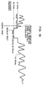
- the pulse generator 66 generates pulses for resetting the phase of a carrier corresponding to the tip portion of a horizontal sync pulse to a reference phase. As illustrated in Fig.
- the phase of the FM carrier corresponding to the tip portion of the horizontal sync pulse is reset to the reference phase.
- resetting causes discontinuous variations in the phase of the FM carrier. Therefore, when these portions are frequency-demodulated, transient distortion occurs.
- the phase of the FM carrier corresponding to the front porch is first reset so that transient distortion occurs at the front porch. Then, when the phase of the FM carrier corresponding to the tip portion of a horizontal sync pulse is reset, discontinuous variations in the phase of the FM carrier do not occur.
- the FM carrier is frequency-converted by an analog multiplier 69.
- a signal (48.6 MHz) sent from a local oscillator 68 to the analog multiplier 69 is synchronous with a master clock.
- the output signal of the analog multiplier 69 is input into a low-pass filter 70 where the FM carrier whose center frequency has shifted to 15.5 MHz while maintaining a frequency deviation ⁇ f at 2.6MHz is separated.
- the center frequency f o of the FM carrier transmitted from the multivibrator 64 is set at 64.1 MHz.
- the reason for setting the frequency at 64.1 MHz is to facilitate the removal of third harmonics which are produced as the output waveform of the multivibrator 64 is a square wave.
- An object of the present invention is to provide a magnetic reproduction apparatus which produces a high-quality image.
- a magnetic reproduction apparatus of the present invention uses a magnetic recording medium on which FM signals produced by frequency-modulating a carrier with wide-band video signals are recorded, and demodulates reproduced signals from the magnetic recording medium into the video signals.
- the magnetic reproduction apparatus is characterized in including a frequency converter for causing the reproduced signals to shift to a higher frequency and a pulse-count-type FM demodulator for demodulating the reproduced signals which have shifted to the higher frequency into the video signals.
- This arrangement restrains the mixing of reproduced signals in the video signals. It is thus possible to obtain the video signals with lessened waveform distortion, thereby achieving a high-quality image.
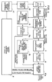
- Figs. 1 and 2 illustrate a first embodiment of the present invention.
- Fig. 1 is a block diagram illustrating the structure of the essential components of a magnetic reproduction apparatus.
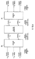
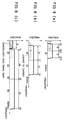
- Fig. 2 illustrates graphs showing the spectrum of output signals from different sections of the magnetic reproduction apparatus of Fig. 1, wherein (a) is the spectrum of an output signal of the head amplifier/equalizer, (b) is the spectrum of an output signal of the analog multiplier, (c) is the spectrum of an output signal of the high-pass filter, and (d) is the spectrum of an output signal of the pulse-count-type FM demodulator.
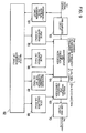
- Fig. 3 is a block diagram illustrating the structure of the essential components of a magnetic reproduction apparatus according to a second embodiment of the present invention.
- Fig. 4 is a block diagram illustrating the structure of the essential components of a magnetic reproduction apparatus according to a third embodiment of the present invention.
- Figs. 5 through 10 illustrate conventional examples.
- Fig. 5 is a block diagram illustrating the structure of a VTR system incorporating a two-channel TCI encoder/decoder.
- Fig. 6 is a timing chart illustrating the relation between the HDTV baseband signals and a line sequenced color-difference TCI signal.
- Fig. 7 illustrates graphs showing the spectrum of signals reproduced by the magnetic reproduction apparatus of Fig. 5, wherein (a) is the spectrum of an FM carrier reproduced from a magnetic tape, (b) is the spectrum of an output signal from the frequency doubler when the FM carrier is input thereto, and (c) is the spectrum of an output signal from the pulse-count-type FM demodulator when the output of the frequency doubler is input thereto.
- Fig. 8 illustrates graphs showing the spectrum of signals reproduced from a magnetic tape, the signals being recorded on the tape after being caused to shift to a lower frequency, wherein (a) is the spectrum of an FM carrier reproduced from the magnetic tape, (b) is the spectrum of an output signal from the frequency doubler when the FM carrier is input thereto, and (c) is the spectrum of an output signal from the pulse-count-type FM demodulator when the output of the frequency doubler is input thereto.
- Fig. 9 is a block diagram illustrating the structure of the essential components of a magnetic reproduction apparatus adopting an FM carrier reset recording method.
- Fig. 10 is a view explaining the process of resetting an FM carrier according to the magnetic reproduction apparatus of Fig. 9.
- reproduced signals from a magnetic tape loaded in a VTR (video tape recorder) 1 are amplified in a head amplifier/equalizer 2 and then input into an analog multiplier 3 for frequency conversion.
- a running speed of the magnetic tape is controlled by a capstan/drum servo circuit 12 based on synchronizing pulses generated by a horizontal/vertical pulse generator 11.
- the horizontal/vertical pulse generator 11 produces the synchronizing pulses according to a clock signal with a frequency of 97.2 MHz, generated by a master clock generator 4.
- An FM carrier is recorded on the magnetic tape with a carrier reset recording method.
- the head amplifier/equalizer 2 outputs a reproduced FM carrier having a center frequency of 15.5 MHz and a bandwidth of 12 MHz as shown in Fig. 2(a).
- a sine wave signal of 24.3 MHz from a local oscillator 5 is input into the analog multiplier 3.
- the sine wave signal is locked with the master clock signal generated by the master clock generator 4.
- the analog multiplier 3 performs the analog multiplication of the sine wave signal and the Fm carrier from the head amplifier/equalizer 2.
- the FM carrier is converted into two FM carriers: an FM carrier of the 8.8-MHz center frequency (obtained by causing the FM carrier to shift to a lower frequency region) and an FM carrier of the 39.8-MHz center frequency (obtained by causing the FM carrier to shift to a higher frequency region). It is arranged that the sine wave signal from the local oscillator 5 substantially does not leak into the output of the multiplier 3.
- the output of the analog multiplier 3 is input into a pulse-count-type FM demodulator 7 via a high-pass filter 6 with a cut-off frequency of 22 MHz. Since the spectrums not higher than 15 MHz are sufficiently attenuated by the high-pass filter 6, the FM carrier, which has shifted to the higher frequency region so as to have the 39.8-MHz center frequency while maintaining the 12-MHz bandwidth, is extracted as illustrated in Fig. 2(c).
- the analog multiplier 3 and the high-pass filter 6 constitute means 20 for causing an FM carrier to shift to a higher frequency region.
- the output of the FM demodulator 7 contains a demodulated signal of the 12-MHz bandwidth, the second higher harmonics of the FM carrier (center frequency: 79.6 MHz, bandwidth: 24 MHz) in the higher frequency region, and the sixth harmonics of the FM carrier in the higher frequency region.
- the output signal of the FM demodulator 7 is input into a low-pass filter 8 whose cut-off frequency is 13 MHz, only the demodulated signal is extracted. Consequently waveform distortion of the demodulated signal decreases.
- the output signal contains higher harmonics other than the above-mentioned higher harmonics. Then, waveform distortion of the demodulated signal occurs. It is therefore advisable to minimize the waveform distortion of the input signal.
- the FM carrier from the head amplifier/equalizer 2 is also input into a reference burst signal detector 9.
- a portion of the FM carrier corresponding to the tip portion of a horizontal sync pulse is extracted, and the extracted portion is hereinafter referred to as a burst signal.
- litter is detected from the burst signal, and a trigger pulse for writing data in a time base corrector (TBC) circuit 10 is generated according to the jitter.
- TBC time base corrector
- the demodulated signal from the low-pass filter 8 is written in the TBC circuit 10 based on the trigger pulse and read out in synchronization with the clock pulse and trigger pulse from the master clock generator. After the time base of the demodulated signal is corrected, the signal is sent as a TCI signal to a TCI decoder (not shown), and thereby luminance signal Y, color-difference signals P R , P B are obtained.
- the reference burst signal detector 9 serves as jitter eliminating means. The following explains elimination of jitter carried out based on the FM carrier which has not yet shifted to the higher frequency region.
- an input signal, S(t), before modulation is a cosine signal with a single frequency, f p , and a fixed amplitude, a
- S(t) a ⁇ cos(2 ⁇ fpt)
- time fluctuation i.e., jitter occurs in the FM carrier reproduced from the magnetic tape.
- jitter the FM carrier is written:
- F c (t+ ⁇ t) A c cos[2 ⁇ f c (t+ ⁇ t)+ ⁇ f/f p .sin ⁇ 2 ⁇ f p (t+ ⁇ t) ⁇ ]
- a demodulated signal, H1 which is obtained by frequency-demodulating or frequency-discriminating G1(t + ⁇ t) extracted by the high-pass filter 6, is
- ⁇ t is caused due to fluctuation in a running speed of the magnetic tape and stretching thereof.
- the jitter spectrum caused by such fluctuation is not higher than several hundred hertz, while the jitter spectrum resulted from the stretching reaches several kilohertz.
- the intensity of spectrum decreases in inversely proportional to frequency.
- F s (t) A c cos(2 ⁇ f s t)
- F s (t + ⁇ t) A c cos ⁇ 2 ⁇ f s (t + ⁇ t) ⁇
- the frequency of an oscillation signal from the local oscillator 5 is set to an integral multiple of the frequency of horizontal pulses, even if moire occurs, it can be stilled on the screen by phase-locking the oscillation signal with the horizontal pulses. Consequently, even if the FM carrier which has not yet shifted to the higher frequency region leaks into the output of the analog multiplier 3 (DU ratio: around 30 dB), the effect is hardly visible.
- a difference between a magnetic reproduction apparatus of this embodiment and !hat of the above-mentioned embodiment is that an oscillation signal of an local oscillator 5a is locked with a trigger pulse from the reference burst signal detector 9.
- the oscillation signal of the local oscillator 5a is input not only into the analog multiplier 3, but also into a TBC circuit 10a as a clock pulse for writing data therein.
- the demodulated signal is denoted as H1(t + ⁇ t) and calculated in a similar manner to the above embodiment
- a difference between a magnetic reproduction apparatus of this embodiment and those of the above-mentioned embodiments is that the apparatus of this embodiment has a second reference burst signal detector 15 for generating a trigger pulse for writing data in the TBC circuit 10a as well as the reference burst signal detector 9.
- a signal corresponding to the tip portion of a horizontal pulse is extracted from the FM carrier which has shifted to the higher frequency region and transmitted from the high-pass filter 6.
- the extracted signal is hereinafter referred to as a second burst signal. Jitter is detected in the second burst signal, and the trigger pulse used for writing data in the TBC circuit 10a is generated based on the jitter.
- G s (t + ⁇ t) A c A o /2 ⁇ cos ⁇ 2 ⁇ (f o +f s )x(t+ ⁇ t) ⁇
Landscapes
- Engineering & Computer Science (AREA)
- Multimedia (AREA)
- Signal Processing (AREA)
- Television Signal Processing For Recording (AREA)
Applications Claiming Priority (2)
| Application Number | Priority Date | Filing Date | Title |
|---|---|---|---|
| JP169914/91 | 1991-07-10 | ||
| JP3169914A JP3053910B2 (ja) | 1991-07-10 | 1991-07-10 | 磁気再生装置 |
Publications (3)
| Publication Number | Publication Date |
|---|---|
| EP0522867A2 true EP0522867A2 (fr) | 1993-01-13 |
| EP0522867A3 EP0522867A3 (en) | 1993-07-07 |
| EP0522867B1 EP0522867B1 (fr) | 1997-03-05 |
Family
ID=15895302
Family Applications (1)
| Application Number | Title | Priority Date | Filing Date |
|---|---|---|---|
| EP92306346A Expired - Lifetime EP0522867B1 (fr) | 1991-07-10 | 1992-07-10 | Dispositif de reproduction magnétique |
Country Status (7)
| Country | Link |
|---|---|
| US (1) | US5377053A (fr) |
| EP (1) | EP0522867B1 (fr) |
| JP (1) | JP3053910B2 (fr) |
| KR (1) | KR960006332B1 (fr) |
| CA (1) | CA2073519C (fr) |
| DE (1) | DE69217750T2 (fr) |
| ES (1) | ES2097880T3 (fr) |
Cited By (1)
| Publication number | Priority date | Publication date | Assignee | Title |
|---|---|---|---|---|
| DE4303469A1 (de) * | 1993-02-06 | 1994-08-11 | Thomson Brandt Gmbh | S-VHS-Videorecorder |
Family Cites Families (17)
| Publication number | Priority date | Publication date | Assignee | Title |
|---|---|---|---|---|
| JPS55154885A (en) * | 1979-05-21 | 1980-12-02 | Olympus Optical Co Ltd | Synchronizing signal separation system |
| JPS56110392A (en) * | 1980-02-06 | 1981-09-01 | Hitachi Ltd | Compensator for fluctuation of time axis |
| JPS58161595A (ja) * | 1982-03-19 | 1983-09-26 | Toshiba Corp | カラ−テレビジヨン信号変換回路 |
| CA1214868A (fr) * | 1982-11-19 | 1986-12-02 | Junzo Tokunaka | Appareil d'enregistrement et/ou de lecture de signaux video et audio |
| US4591930A (en) * | 1983-09-23 | 1986-05-27 | Eastman Kodak Company | Signal processing for high resolution electronic still camera |
| US4843334A (en) * | 1986-12-09 | 1989-06-27 | Canon Kabushiki Kaisha | Frequency demodulator operable with low frequency modulation carriers |
| JPS63185177A (ja) * | 1987-01-27 | 1988-07-30 | Sony Corp | 周波数変調回路 |
| US5045950A (en) * | 1987-05-01 | 1991-09-03 | Sharp Kabushiki Kaisha | Circuit for detecting and compensating for jitter produced by a recording/reproducing apparatus |
| JPH01264492A (ja) * | 1988-04-15 | 1989-10-20 | Sharp Corp | Vtr記録再生映像信号のジッタ検出装置 |
| JPH0632467B2 (ja) * | 1987-05-01 | 1994-04-27 | シャープ株式会社 | Vtr記録再生映像信号のジッタ検出方法 |
| JPS6482572A (en) * | 1987-09-24 | 1989-03-28 | Mitsubishi Electric Corp | Gaas solar cell |
| JPH01305785A (ja) * | 1988-06-03 | 1989-12-11 | Sharp Corp | ジッタ補正装置 |
| US4987491A (en) * | 1989-01-20 | 1991-01-22 | Sanyo Electric Co., Ltd. | Jitter compensation circuit for processing jitter components of reproduced video signal |
| US5062005A (en) * | 1989-02-01 | 1991-10-29 | Matsushita Electric Industrial Co., Ltd. | Videodisc reproducing apparatus |
| JPH02218278A (ja) * | 1989-02-20 | 1990-08-30 | Sony Corp | Fm変調回路 |
| JP2507821B2 (ja) * | 1990-03-13 | 1996-06-19 | シャープ株式会社 | キャリアリセットfm変調器 |
| JPH0481181A (ja) * | 1990-07-23 | 1992-03-13 | Sony Corp | ビデオディスク再生装置 |
-
1991
- 1991-07-10 JP JP3169914A patent/JP3053910B2/ja not_active Expired - Lifetime
-
1992
- 1992-07-08 US US07/910,757 patent/US5377053A/en not_active Expired - Fee Related
- 1992-07-09 KR KR1019920012195A patent/KR960006332B1/ko not_active Expired - Fee Related
- 1992-07-09 CA CA002073519A patent/CA2073519C/fr not_active Expired - Fee Related
- 1992-07-10 EP EP92306346A patent/EP0522867B1/fr not_active Expired - Lifetime
- 1992-07-10 ES ES92306346T patent/ES2097880T3/es not_active Expired - Lifetime
- 1992-07-10 DE DE69217750T patent/DE69217750T2/de not_active Expired - Fee Related
Cited By (2)
| Publication number | Priority date | Publication date | Assignee | Title |
|---|---|---|---|---|
| DE4303469A1 (de) * | 1993-02-06 | 1994-08-11 | Thomson Brandt Gmbh | S-VHS-Videorecorder |
| DE4303469B4 (de) * | 1993-02-06 | 2005-11-10 | Deutsche Thomson-Brandt Gmbh | S-VHS-Videorecorder |
Also Published As
| Publication number | Publication date |
|---|---|
| CA2073519A1 (fr) | 1993-01-11 |
| JPH0520787A (ja) | 1993-01-29 |
| EP0522867A3 (en) | 1993-07-07 |
| US5377053A (en) | 1994-12-27 |
| DE69217750T2 (de) | 1997-09-04 |
| KR960006332B1 (ko) | 1996-05-13 |
| EP0522867B1 (fr) | 1997-03-05 |
| CA2073519C (fr) | 1997-01-21 |
| KR930003017A (ko) | 1993-02-23 |
| ES2097880T3 (es) | 1997-04-16 |
| DE69217750D1 (de) | 1997-04-10 |
| JP3053910B2 (ja) | 2000-06-19 |
Similar Documents
| Publication | Publication Date | Title |
|---|---|---|
| JPH0115235B2 (fr) | ||
| KR920003937B1 (ko) | VTR 기록재생 영상신호의 지터(jitter) 검출방법 및 검출장치 | |
| JP3110107B2 (ja) | 周波数重畳情報挿入及び分離回路とその情報発生方法 | |
| JPS645516B2 (fr) | ||
| JPS59186492A (ja) | カラ−映像信号記録再生装置 | |
| EP0522867B1 (fr) | Dispositif de reproduction magnétique | |
| US4593327A (en) | Color video signal recording and/or reproducing system | |
| JPS59172898A (ja) | カラ−映像信号再生装置におけるクロツクパルス発生回路 | |
| RU2072565C1 (ru) | Устройство для записи-воспроизведения опорного сигнала корректора временных искажений в видеомагнитофоне | |
| JPS6337998B2 (fr) | ||
| KR900001450B1 (ko) | 기록 재생 장치 | |
| KR880000412Y1 (ko) | 칼러 영상신호 기록장치 | |
| JPH0654970B2 (ja) | 映像信号記録再生装置 | |
| JPH04245892A (ja) | クランプ装置 | |
| JPS6364488A (ja) | 磁気記録再生方式 | |
| JPH0578996B2 (fr) | ||
| JPH0144075B2 (fr) | ||
| JPS6313631B2 (fr) | ||
| JP2627299B2 (ja) | 光学式記録再生方式 | |
| JPS605117B2 (ja) | カラービデオ信号の記録再生方式 | |
| JPS634393B2 (fr) | ||
| JPS62224189A (ja) | 映像信号記録再生装置 | |
| JPH0224437B2 (fr) | ||
| JPS5859692A (ja) | 搬送色信号の記録装置 | |
| JPS6029099A (ja) | 記録再生装置 |
Legal Events
| Date | Code | Title | Description |
|---|---|---|---|
| PUAI | Public reference made under article 153(3) epc to a published international application that has entered the european phase |
Free format text: ORIGINAL CODE: 0009012 |
|
| AK | Designated contracting states |
Kind code of ref document: A2 Designated state(s): DE ES FR GB NL |
|
| PUAL | Search report despatched |
Free format text: ORIGINAL CODE: 0009013 |
|
| AK | Designated contracting states |
Kind code of ref document: A3 Designated state(s): DE ES FR GB NL |
|
| 17P | Request for examination filed |
Effective date: 19930927 |
|
| GRAG | Despatch of communication of intention to grant |
Free format text: ORIGINAL CODE: EPIDOS AGRA |
|
| 17Q | First examination report despatched |
Effective date: 19960403 |
|
| GRAH | Despatch of communication of intention to grant a patent |
Free format text: ORIGINAL CODE: EPIDOS IGRA |
|
| GRAH | Despatch of communication of intention to grant a patent |
Free format text: ORIGINAL CODE: EPIDOS IGRA |
|
| GRAA | (expected) grant |
Free format text: ORIGINAL CODE: 0009210 |
|
| AK | Designated contracting states |
Kind code of ref document: B1 Designated state(s): DE ES FR GB NL |
|
| REF | Corresponds to: |
Ref document number: 69217750 Country of ref document: DE Date of ref document: 19970410 |
|
| ET | Fr: translation filed | ||
| REG | Reference to a national code |
Ref country code: ES Ref legal event code: FG2A Ref document number: 2097880 Country of ref document: ES Kind code of ref document: T3 |
|
| PLBE | No opposition filed within time limit |
Free format text: ORIGINAL CODE: 0009261 |
|
| STAA | Information on the status of an ep patent application or granted ep patent |
Free format text: STATUS: NO OPPOSITION FILED WITHIN TIME LIMIT |
|
| 26N | No opposition filed | ||
| REG | Reference to a national code |
Ref country code: GB Ref legal event code: IF02 |
|
| PGFP | Annual fee paid to national office [announced via postgrant information from national office to epo] |
Ref country code: FR Payment date: 20020709 Year of fee payment: 11 |
|
| PGFP | Annual fee paid to national office [announced via postgrant information from national office to epo] |
Ref country code: GB Payment date: 20020710 Year of fee payment: 11 |
|
| PGFP | Annual fee paid to national office [announced via postgrant information from national office to epo] |
Ref country code: DE Payment date: 20020717 Year of fee payment: 11 |
|
| PGFP | Annual fee paid to national office [announced via postgrant information from national office to epo] |
Ref country code: ES Payment date: 20020726 Year of fee payment: 11 |
|
| PGFP | Annual fee paid to national office [announced via postgrant information from national office to epo] |
Ref country code: NL Payment date: 20020730 Year of fee payment: 11 |
|
| PG25 | Lapsed in a contracting state [announced via postgrant information from national office to epo] |
Ref country code: GB Free format text: LAPSE BECAUSE OF NON-PAYMENT OF DUE FEES Effective date: 20030710 |
|
| PG25 | Lapsed in a contracting state [announced via postgrant information from national office to epo] |
Ref country code: ES Free format text: LAPSE BECAUSE OF NON-PAYMENT OF DUE FEES Effective date: 20030711 |
|
| PG25 | Lapsed in a contracting state [announced via postgrant information from national office to epo] |
Ref country code: NL Free format text: LAPSE BECAUSE OF NON-PAYMENT OF DUE FEES Effective date: 20040201 |
|
| PG25 | Lapsed in a contracting state [announced via postgrant information from national office to epo] |
Ref country code: DE Free format text: LAPSE BECAUSE OF NON-PAYMENT OF DUE FEES Effective date: 20040203 |
|
| GBPC | Gb: european patent ceased through non-payment of renewal fee |
Effective date: 20030710 |
|
| PG25 | Lapsed in a contracting state [announced via postgrant information from national office to epo] |
Ref country code: FR Free format text: LAPSE BECAUSE OF NON-PAYMENT OF DUE FEES Effective date: 20040331 |
|
| NLV4 | Nl: lapsed or anulled due to non-payment of the annual fee |
Effective date: 20040201 |
|
| REG | Reference to a national code |
Ref country code: FR Ref legal event code: ST |
|
| REG | Reference to a national code |
Ref country code: ES Ref legal event code: FD2A Effective date: 20030711 |