EP0523917A2 - Epitaxie par couches mono-atomiques d'un semi-conducteur composé - Google Patents
Epitaxie par couches mono-atomiques d'un semi-conducteur composé Download PDFInfo
- Publication number
- EP0523917A2 EP0523917A2 EP92306314A EP92306314A EP0523917A2 EP 0523917 A2 EP0523917 A2 EP 0523917A2 EP 92306314 A EP92306314 A EP 92306314A EP 92306314 A EP92306314 A EP 92306314A EP 0523917 A2 EP0523917 A2 EP 0523917A2
- Authority
- EP
- European Patent Office
- Prior art keywords
- supplying
- crystalline substrate
- compound semiconductor
- source
- iii
- Prior art date
- Legal status (The legal status is an assumption and is not a legal conclusion. Google has not performed a legal analysis and makes no representation as to the accuracy of the status listed.)
- Withdrawn
Links
Images





Classifications
-
- H—ELECTRICITY
- H10—SEMICONDUCTOR DEVICES; ELECTRIC SOLID-STATE DEVICES NOT OTHERWISE PROVIDED FOR
- H10P—GENERIC PROCESSES OR APPARATUS FOR THE MANUFACTURE OR TREATMENT OF DEVICES COVERED BY CLASS H10
- H10P14/00—Formation of materials, e.g. in the shape of layers or pillars
- H10P14/20—Formation of materials, e.g. in the shape of layers or pillars of semiconductor materials
- H10P14/29—Formation of materials, e.g. in the shape of layers or pillars of semiconductor materials characterised by the substrates
- H10P14/2901—Materials
- H10P14/2907—Materials being Group IIIA-VA materials
- H10P14/2909—Phosphides
-
- H—ELECTRICITY
- H10—SEMICONDUCTOR DEVICES; ELECTRIC SOLID-STATE DEVICES NOT OTHERWISE PROVIDED FOR
- H10P—GENERIC PROCESSES OR APPARATUS FOR THE MANUFACTURE OR TREATMENT OF DEVICES COVERED BY CLASS H10
- H10P14/00—Formation of materials, e.g. in the shape of layers or pillars
- H10P14/20—Formation of materials, e.g. in the shape of layers or pillars of semiconductor materials
- H10P14/24—Formation of materials, e.g. in the shape of layers or pillars of semiconductor materials using chemical vapour deposition [CVD]
-
- H—ELECTRICITY
- H10—SEMICONDUCTOR DEVICES; ELECTRIC SOLID-STATE DEVICES NOT OTHERWISE PROVIDED FOR
- H10P—GENERIC PROCESSES OR APPARATUS FOR THE MANUFACTURE OR TREATMENT OF DEVICES COVERED BY CLASS H10
- H10P14/00—Formation of materials, e.g. in the shape of layers or pillars
- H10P14/20—Formation of materials, e.g. in the shape of layers or pillars of semiconductor materials
- H10P14/29—Formation of materials, e.g. in the shape of layers or pillars of semiconductor materials characterised by the substrates
- H10P14/2901—Materials
- H10P14/2907—Materials being Group IIIA-VA materials
- H10P14/2911—Arsenides
-
- H—ELECTRICITY
- H10—SEMICONDUCTOR DEVICES; ELECTRIC SOLID-STATE DEVICES NOT OTHERWISE PROVIDED FOR
- H10P—GENERIC PROCESSES OR APPARATUS FOR THE MANUFACTURE OR TREATMENT OF DEVICES COVERED BY CLASS H10
- H10P14/00—Formation of materials, e.g. in the shape of layers or pillars
- H10P14/20—Formation of materials, e.g. in the shape of layers or pillars of semiconductor materials
- H10P14/32—Formation of materials, e.g. in the shape of layers or pillars of semiconductor materials characterised by intermediate layers between substrates and deposited layers
- H10P14/3242—Structure
- H10P14/3244—Layer structure
- H10P14/3251—Layer structure consisting of three or more layers
- H10P14/3252—Alternating layers, e.g. superlattice
-
- H—ELECTRICITY
- H10—SEMICONDUCTOR DEVICES; ELECTRIC SOLID-STATE DEVICES NOT OTHERWISE PROVIDED FOR
- H10P—GENERIC PROCESSES OR APPARATUS FOR THE MANUFACTURE OR TREATMENT OF DEVICES COVERED BY CLASS H10
- H10P14/00—Formation of materials, e.g. in the shape of layers or pillars
- H10P14/20—Formation of materials, e.g. in the shape of layers or pillars of semiconductor materials
- H10P14/34—Deposited materials, e.g. layers
- H10P14/3402—Deposited materials, e.g. layers characterised by the chemical composition
- H10P14/3414—Deposited materials, e.g. layers characterised by the chemical composition being group IIIA-VIA materials
- H10P14/3418—Phosphides
-
- H—ELECTRICITY
- H10—SEMICONDUCTOR DEVICES; ELECTRIC SOLID-STATE DEVICES NOT OTHERWISE PROVIDED FOR
- H10P—GENERIC PROCESSES OR APPARATUS FOR THE MANUFACTURE OR TREATMENT OF DEVICES COVERED BY CLASS H10
- H10P14/00—Formation of materials, e.g. in the shape of layers or pillars
- H10P14/20—Formation of materials, e.g. in the shape of layers or pillars of semiconductor materials
- H10P14/34—Deposited materials, e.g. layers
- H10P14/3402—Deposited materials, e.g. layers characterised by the chemical composition
- H10P14/3414—Deposited materials, e.g. layers characterised by the chemical composition being group IIIA-VIA materials
- H10P14/3421—Arsenides
-
- Y—GENERAL TAGGING OF NEW TECHNOLOGICAL DEVELOPMENTS; GENERAL TAGGING OF CROSS-SECTIONAL TECHNOLOGIES SPANNING OVER SEVERAL SECTIONS OF THE IPC; TECHNICAL SUBJECTS COVERED BY FORMER USPC CROSS-REFERENCE ART COLLECTIONS [XRACs] AND DIGESTS
- Y10—TECHNICAL SUBJECTS COVERED BY FORMER USPC
- Y10S—TECHNICAL SUBJECTS COVERED BY FORMER USPC CROSS-REFERENCE ART COLLECTIONS [XRACs] AND DIGESTS
- Y10S148/00—Metal treatment
- Y10S148/048—Energy beam assisted EPI growth
-
- Y—GENERAL TAGGING OF NEW TECHNOLOGICAL DEVELOPMENTS; GENERAL TAGGING OF CROSS-SECTIONAL TECHNOLOGIES SPANNING OVER SEVERAL SECTIONS OF THE IPC; TECHNICAL SUBJECTS COVERED BY FORMER USPC CROSS-REFERENCE ART COLLECTIONS [XRACs] AND DIGESTS
- Y10—TECHNICAL SUBJECTS COVERED BY FORMER USPC
- Y10S—TECHNICAL SUBJECTS COVERED BY FORMER USPC CROSS-REFERENCE ART COLLECTIONS [XRACs] AND DIGESTS
- Y10S148/00—Metal treatment
- Y10S148/072—Heterojunctions
Definitions
- the present invention relates to a process for growing a crystalline compound semiconductor.
- Compound semiconductors are used, for example, as materials for composing various electronic devices, and for a miniaturization and improvement of the performance of electronic devices, sometimes it is desirable to grow a compound semiconductor having a required composition to a required thickness at a required place.
- the atomic layer epitaxy (ALE) process for controlling the growth at an atomic layer level is one means of attaining the above requirements.
- MOCVD metalorganic chemical vapor deposition
- MBE molecular beam epitaxy
- ALE atomic layer epitaxy
- the MOCVD provides a high deposition rate, but in a MOCVD, it is difficult to control the atomic layer level.
- the MBE uses a super high vacuum apparatus, wherein a molecule beam is fed into a super high vacuum chamber to grow a crystal layer.
- ALE is advantageous when a ternary element compound semiconductor is grown.
- the three elements occupy random sites in the crystal so that scattering of a carrier is caused by the alloy effect.
- the site of each element can be designed by ALE so that a crystal structure without the alloy scattering effect can be grown.
- Japanese Unexamined Patent Publication (Kokai) No. 61-34922 discloses an ALE in which a vacuum chamber is evacuated to a super high vaccum, an As substrate is heated, and gases containing constituent elements for a compound semiconductor to be grown are sequentially introduced in predetermined amounts into the vaccum chamber, to grow a compound molecular layer by molecular layer.
- This process requires a long time for switching the source gas, during which the once-deposited atomic layer may be adversely affected, and thus the controllability thereof is low.
- the ALE has problems with hetero epitaxy.
- an epitaxial growth of an InAs layer on an InAs substrate is described.
- an InAs substrate is heated to, for example, 350°C, and a source gas for a III-group element, In, and a source gas for a V-group element, As, are alternately introduced over the substrate.
- the gas pressures are, for example, in a range of several torr to several 100 torr.
- An example of the In source is trimethylindium (CH3)In
- an example of the Ga source is arsine AsH3.
- An In layer and an As layer are alternately grown on the substrate, to thereby grow an InAs crystal by ALE.
- a GaAs crystal is grown, for example, at 500°C, from trimethylgallium (CH3)Ga, as a Ga source and arsine AsH3 as an As source.
- CH3Ga trimethylgallium
- AsH3 arsine AsH3
- the growth temperature of an InAs crystal is 350°C and that of a GaAs crystal is 500°C. Accordingly, when a heterojunction of InAs/GaAs is grown, if the growth temperature is set to 500°C it is too high for the InAs growth, and accordingly, the self-limiting effect is lost and an atomic layer growth becomes difficult. Further, if the growth temperature is set to 350°C it is too low for the GaAs growth, and thus crystal growth does not proceed. If the growth temperature is frequently varied during the crystal growth, the controllability and efficiency thereof are deteriorated.
- the growth rate by one cycle of source gas supply is determined by the concentrations and supply times of the source gases.
- the growth rate in ALE is reported, for example, for GaAs in Applied Physics Letters, vol. 53, pp. 1509-1511 (1988).
- the purity of a GaAs crystal depending on the concentrations and supply times of the III and V source gases is reported in Journal of Crystal Growth, vol. 93, p. 557 (1988).
- the effects of the time when a source gas is not supplied on the growth rate and the characteristics of the grown crystal are not known.
- the atomic layer epitaxy, particularly hetero-epitaxy of a compound semiconductor has not been clarified as yet, and it is still difficult to grow a crystal having required qualities by ALE.
- an object of the present invention is to provide a process for growing a crystalline compound semiconductor, in which a control of an atomic layer level is possible and an excellent crystalline compound semiconductor can be grown.
- Another object of the present invention is to provide a process for growing a heterojunction of crystalline compound semiconductors containing indium as the III-group element in an atomic layer precision.
- a further object of the present invention is to examine the effects of the time at which a source gas is not supplied to the crystal growth, and to improve the ALE technology and enable a control of the growth of a crystal at the atom level and provide an excellent hetero-epitaxy.
- the present invention provides a process for growing a crystalline compound semiconductor, comprising the steps of heating a crystalline substrate to a predetermined temperature in a vacuum chamber; and at said predetermined temperature of the crystalline substrate, in the following sequence; supplying a first source gas for a III-group element containing an organic In compound diluted with hydrogen over said crystalline substrate under a predetermined pressure, discharging the first source gas, supplying a second source gas for a first V-group element over said crystalline substrate under a predetermined pressure, discharging the second source gas, supplying a third source gas for a III-group element containing an organic In compound diluted with hydrogen over said crystalline substrate under a predetermined pressure, discharging the third source gas, supplying a forth source for a second V-group element over said crystalline substrate under a predetermined pressure, and discharging the forth source gas, wherein said first and second V-group elements have at least different compositions or even contains different elements.
- the first and second V-group elements have at least different compositions or even
- the steps of supplying the first and second source gases can be alternately repeated to grow a first compound semiconductor layer on the crystalline substrate, before the step of supplying the third source gas.
- the steps of supplying the third and fourth source gases can be alternately repeated to grow a second compound semiconductor layer, on said first compound semiconductor layer.
- heterojunction such as InAs/InP, InAsP/InP, InAs/InAsP can be grown.
- the first and third source gases are supplied over the crystalline substrate under the conditions of a predetermined temperature, a rate of hydrogen dilution of the organic In compound, a flow rate of the source gas and a predetermined pressure such that the organic In compound is not effectively pyrolized before reaching the crystalline substrate, but is pyrolized on reaching the crystalline substrate.
- a hydrogen gas is supplied after the step of supplying each source gas, to purge away the source gas, but the time for which the H2 is supplied for the purge, after the supply of a V-group source gas, is limited within a certain range such that the already adsorbed V-group atoms are not removed.
- a process for growing a crystalline compound semiconductor comprising the steps of supplying a III-group element source gas over a crystalline substrate, supplying a hydrogen gas over the crystalline substrate to purge away the III-group element source gas for a predetermined time, supplying a V-group element source gas over the crystalline substrate, and supplying a hydrogen gas over the crystalline substrate to purge away the V-group element source gas for a predetermined time, and repeating said steps to thereby grow a III-V compound semiconductor layer on the crystalline substrate, wherein said time of supplying the hydrogen gas for said purge is controlled, to thereby control a growth rate of said compound semiconductor.
- a process for growing a crystalline compound semiconductor comprising the steps of supplying a III-group element source gas over a crystalline substrate, supplying a hydrogen gas over the crystalline substrate to purge away the III-group element source gas for a predetermined time, supplying supplying a V-group element source gas over the crystalline substrate, supplying a hydrogen gas over the crystalline substrate to purge away the V-group source gas, and supplying a dopant source over the crystalline substrate, and repeating the above steps to thereby grow a doped III-V compound semiconductor layer on the crystalline substrate for a predetermined time, wherein said time of supplying the hydrogen gas is controlled to thereby control a concentration of said dopant in said doped-III-V compound semiconductor layer.
- a semiconductor device comprising a structure of alternate first and second III-V compound semiconductor layers, said first and second III-V compound semiconductor layers containing indium as a constituent element having a different composition or constituent element, said first and second III-V compound semiconductor layers having a thickness of not more than 20 molecules of the III-V compound semiconductor thereof.
- InAs has a high electron mobility
- lattice mismatched type and heterojunction type devices utilizing InAs are extremely useful, but it has not been easy to form such a heterojunction.
- the composition of In in InGaAs is at most only about 0.2 (20 mole% of InGaAs).
- the present inventor carefully studied a system of a heterojunction containing indium in both sides, which includes systems having a small lattice mismatch and makes the growth of the heterojunction easier.
- InP/InAs is advantageous since the interdiffusion of As and P at the interface of InP and InAs is extremely small.
- In-containing compound semiconductors include combinations thereof which have close growth temperature ranges in ALE.
- a III-group source gas comprising an organic In compound diluted with hydrogen is used under a predetermined pressure, and this enables a growth of a mono atomic layer of indium on a crystalline substrate.
- the reaction of the source gas can be controlled by setting a temperature of the crystalline substrate. Particularly, it is possible to control the reaction such that the organic In compound is not pyrolized until it reaches the substrate, i.e., is pyrolized on the substrate.
- This control is made possible by using a source gas of an organic In compound diluted with hydrogen.
- the combination of the utilization of a hydrogen-diluted organic In compound and the control of the substrate temperature makes a two-dimensional growth of In or an In-containing III-group elements possible. If the substrate temperature is too high, a three-dimensional deposition occurs.
- a separation between a III-group source gas and a V-group source gas can be improved by supplying a hydrogen gas, for purging, between the steps of supplying the III-group and V-group gases.
- a hydrogen gas for purging By utilizing a hydrogen gas for purging, the separation of the different source gases is made more complete in a shorter time, and this prevents damage to the once formed complete interface during the gas separation period which occurs in the gas separation by the super high vacuum, as taught in Japanese Unexamined Patent Publication (Kokai) No. 61-34922.
- the process of the present invention widens the ranges of controllable conditions for obtaining a desirable heterojunction of various compound semiconductors.
- the growth of an excellent heterojunection of, for example, InAs/InP by ALE is made possible by the present invention.
- the purging should be kept within the certain time needed for obtaining an excellent crystal or heterojunction. Nevertheless, the amounts of vacancies, dopants, etc., in the compound semiconductor can be controlled by controlling the purge time, since the amount of the V-group element desorped by the purge depends on the purge time.
- Fig. 1 schematically shows an apparatus for carrying out the crystal growth process of the present invention
- Fig. 2 shows the dependency of the crystal growth rate on the growth temperature.
- a reaction tube 1 is made of quartz, has a narrowed end, and can be evacuated.
- a susceptor 8 for mounting a crystalline substrate thereon is arranged in the reaction tube 1.
- the susceptor 8 is made of, for example, carbon (graphite), able to absorb a radio frequency.
- the susceptor 8 is supported by a support bar 11 and is movable between a preparation chamber 13 and a crystal growth chamber, through a gate valve 12.
- Bellows 14 are provided to maintain an airtight condition while vertically moving the support bar 11.
- An RF coil 2 is arranged around the reaction tube 1 at the portion at which the crystal growth is carried out, and the carbon susceptor 8 can be heated by RF.
- the lower portion of the reaction tube 1 is connected to a gas inlet 15 having a small diameter, to thus increase the speed of a gas stream or jet.
- the gas inlet 15 is connected to a manifold 5, for selecting a gas from among a plurality of gases.
- the gas inlet portion 6 of the manifold 5 is connected to a plurality of gas pipes.
- the manifold 5 also has a vent pipe 7 through which supplied gases can escape without being supplied to the reaction tube 1.
- a valve 4 for regulating a pressure and a vacuum unit 3 for evacuating the used gas.
- this apparatus it is possible to heat the crystalline substrate to a predetermined temperature, to supply a desired source gas over the substrate at a desired flow rate under a desired pressure, and to exchange one gas for another gas in a desired short time.
- the heating means may be an electrical resistance heating, lamp heating or any other heating means, and the reaction tube 1 may be made a material of other than quartz.
- the susceptor 8 may be any such element capable of holding the substrate at a predetermined temperature.
- the manifold 5 should be able to exchange on gas charged in the reaction tube for another gas in about 10 seconds.
- a crystal growth was carried out to grow InAs on a (1 0 0) plane InAs substrate and InP on a (1 0 0) plane InP substrate.
- the growth conditions were as follows.
- the In source was trimethylindium (TMIn), the As source was arsine (AsH3), and the P source was phosphine (PH3).
- the In source gas was obtained by passing hydrogen gas through TMIn in a container kept at 27.1°C, and was supplied into the reaction tube 1 together with hydrogen at 60 sccm for 15 seconds.
- the concentration of TMIn was about 5x10 ⁇ 3% in the reactor and 0.17% in the TMIn container.
- AsH3 was diluted with hydrogen to about 10%, and supplied at 480 sccm for 10 seconds.
- PH3 was diluted with hydrogen to about 20%, and supplied at 480 sccm for about 20 seconds.
- the pressure in the reaction tube 1 was kept at about 15 torr during the crystal growth.
- the total gas flow in tube was 2000 sccm.
- the gas supply was carried out in the order of the III-group element source, hydrogen, the V-group element source and hydrogen, and this cycle was repeated.
- the hydrogen was supplied as a purging gas, to prevent a mixing of the III-group and V-group element sources in the reaction tube 1.
- Fig. 2 shows the results of the obtained growth rate in relation to the growth temperature.
- One cycle of gas supply involves one supply of the III-group element source and one supply of the V-group element source, and the growth rate is expressed by the number of molecular layers grown per cycle.
- Fig. 2 clearly demonstrates that one molecular layer of InAs was grown in one cycle in a temperature range of about 350 to 450°C, preferably about 310 to 450°C, and half of a molecular layer of InP was grown in one cycle in a temperature range of about 300 to 450°C, preferably 310 to 425°C. It is a characteristic of InP that a half molecular layer is grown in one cycle, and thus two cycles are necessary when growing one molecular layer of InP.
- the temperature ranges in which InAs and InP can be stably grown under a precise control almost overlap each other, and thus InAs and InP layers can be grown on a crystalline substrate kept at a certain temperature to thereby form an excellent heterojunection.
- the growth temperature was kept constant at 365°C and the pressure was kept constant at 15 torr, during the crystal growth.
- the In source was TMIn diluted with hydrogen to about 0.17%; the As source was AsH3 diluted with hydrogen to about 10%, and the P source was PH3 diluted with hydrogen to about 20%.
- the flow rates of the In source, As source, and P source were 60 sccm, 250 sccm, and 400 sccm, respectively.
- Hydrogen gas was further added as a carrier gas, to make the total gas flow rate in the reaction tube 1 to 2000 sccm.
- InAs and InP layers were grown to determine the time needed for supplying the In source.
- Fig. 3 shows the dependency of the growth rates of InAs and InP on the pulse time width of the In source (TMIn) supply. It was found that a TMIn supply of at least about 4 seconds is sufficient to grow a complete molecular layer of InAs. Also, a TMIn supply of at least about 7 seconds is sufficient to grow a complete half molecular layer of InP, and two gas supply cycles provide a complete molecular layer of InP.
- TMIn In source
- the TMIn supply time was set to 12 seconds.
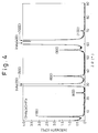
- Fig. 4 is an X-ray diffraction pattern of (InAs)3(InP)2.
- the peaks (1 0 0), (4 0 0), (6 0 0), (9 0 0) and (11 0 0) are satellite peaks and indicate that a good single molecular layer growth occurred.
- the peaks (5 0 0) and (10 0 0) are diffraction peaks from the five molecular layers as a unit, and include peaks (2 0 0) and (4 0 0) of InAs of the substrate.
- Fig. 5 shows an X-ray diffraction pattern of a superlattice structure (InAs)3(InP)1 made in the same manner as above.
- four molecular layers are the repeating unit and (4 0 0) and (8 0 0) peaks are derived from this repeating unit.
- the peaks (1 0 0), (3 0 0), (5 0 0), (7 0 0) and (9 0 0) are satellite peaks derived from the single molecular layer structure.
- Fig. 6 shows an X-ray diffraction pattern of a superlattice structure (InAs)2(InP)1 made in the same manner as above. In this pattern, satellite peaks derived from the single molecular layer structure are observed.
- Figs. 4 to 6 The X-ray peaks shown in Figs. 4 to 6 were obtained from the grown layer having a thickness of about 100 nm. It was confirmed from these figures that the superlattice structures as designed were made.
- TMIn a III-group element source
- TMIn a III-group element source
- To pyrolize TMIn hydrogen is needed, and thus methyl is converted to methane.
- the hydrogen of the carrier gas supplies this hydrogen to react with methyl.
- Fig. 7 shows this reaction, wherein R stands for methyl and the white circle stands for indium.
- TMIn trimethyl indium
- the adsorption energy is so low that the adsorbed In atom is desorped into the atmosphere. To ensure this, it is important that the temperature of the substrate is not too high.
- the In atom adsorped by pyrolysis of a TMIn molecule on the substrate migrates on the surface of the substrate to be stabilized where the In atoms aggregate or come in contact. Thus, the In atom layer expands to form the two-dimensional growth.
- the substrate temperature or growth temperature the dilution rate of TMIn by hydrogen, the time that TMIn reaches to the crystalline substrate from the source, i.e., the flow rate of the supply gas if the reaction chamber is fixed, and the frequency of the collision of the TMIn molecules in the atmosphere, i.e., the pressure of the supply gas, and the like, are the parameters for the control of the considered reaction mechanism.
- TMIn is little pyrolized in the atmosphere before reaching the substrate, is adsorbed in the form of a molecule on the substrate, and is pyrolized by hydrogen to become an In atom, and form an In atom layer.
- the source gas may be, for example, molecules of III-group and V-group elements bonded with any of hydrogen, methyl, ethyl, isobutyl, tertiarybutyl, amino, and some halogens.
- the V-group element may be not only As and P but also other V-group elements such as Sb. Sb allows a control of the lattice constant mismatch.
- Figs. 8A to 8D show the homogeneous growth of GaAs from trimethyl gallium (TMGa) and arsine (AsH3) in hydrogen gas flows.
- Fig. 8A shows AsH3 as an As source being supplied on a crystalline substrate.
- AsH3 is pyrolized by the catalytic action of the crystal surface of the substrate to become an As atom or molecule and deposit one atomic layer on the crystal surface. Since As has a high vapor pressure or a small bond energy of As-As, more than one atomic layer are not adsorped.
- the AsH3 supply is stopped and only hydrogen gas is supplied to purge away the AsH3 molecule.
- H2 As atoms are desorped the GaAs surface and the number of the remaining As atoms depends on the time of H2 purge and the substrate temperature.
- TMGa When TMGa is supplied, the TMGa molecules react selectively with the As atoms on the surface of the substrate, to adsorp Ga atoms thereon (Fig. 8C).
- the amount or rate of the crystal growth after the cycle (AsH3 ⁇ H2 ⁇ TMGa ⁇ H2) of Figs. 8A to 8C is determined by the amount of As atoms remaining on the surface of the substrate after a take off thereof.
- the effect of the desorption of the V-group element by the hydrogen purging step causes only a variation of the growth rate of the compound semiconductor.
- the desorption of a V-group element affects the precision of the heterojunction and alloying layers appear at the interface of the hetero compound semiconductors.
- the alloy layer may cause scattering, and accordingly, the desorption of the V-group element must be prevented to thereby obtain a perfect atomic layer heterojunction.
- the amount of doping or the efficiency of the dopant can be controlled.
- the control of other impurities (donor, acceptor) to be incorporated or a point defect density, etc. is possible.
- Fig. 1 An apparatus as shown in Fig. 1 was used.
- the source gases were TMIn and AsH3 diluted with H2 and supplied onto an InAs crystalline substrate.
- the pressure in the reaction tube was kept at 15 torr and the total gas flow rate was 2000 cc/min during the growth.
- H2 was passed through a cylinder containing TMIn kept at 27°C at 60 cc/min.
- AsH3 diluted with H2 to 10% was supplied at 480 cc/min.
- Fig. 9A shows the sequential chart of the gas supply.
- t1 denotes the time of H2 purge after AsH3 supply
- t2 denotes the time of H2 purge after TMIn purge.
- the exchange of the TMIn and AsH3 was performed by the high speed switchable valve of the manifold.
- t1 and t2 show the growth rates in relation to t1 and t2 at a growth temperature of 400°C.
- the TMIn supply was 5 seconds and the AsH3 supply was 10 seconds, in one cycle.
- One of t1 and t2 was always fixed to 0.5 second.
- Fig. 10 demonstrates that the growth rate per cycle decreases with an increase of the H2 purge time after the AsH3 supply, and is not altered by an increase of the H2 purge time after the TMIn supply.
- Fig. 12 shows the growth rate of InAs v.s. the pulse time of the TMIn supply, with t1 as a parameter, in an ALE at 400°C. It is seen that the growth rate of InAs by ALE is controlled by t1, i.e., the pulse time of the purge after the AsH3 supply.
- H2Se was supplied after the H2 purge step (t1) after AsH3 supply, to determine the doped amount.
- H2Se diluted with H2 to 10 ppm was supplied at 30 cc/min for 1 second.
- Fig. 13 shows the electron concentration (Se concentration) of the obtained crystal v.s. t1. It is demonstrated that the electron concentration (Se conc.) increases along with an increase of t1.
- the dopant gas is supplied alone or in combination with a III-group element source, after the H2 purge following the V-group element source supply, although it is not limited thereto.
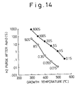
- Fig. 14 shows the limit of the time of the H2 purge after an As source supply for preventing a desorption of the already deposited As, in relation to the growth temperature.
- the conditions of the process were the same as those for Fig. 2.
- the preferable time limit of the pulse time t of H2 purge can be expressed by the formula (1), more preferably by the formula (2). log t ⁇ -(7.09/475)T + 7.33 log t ⁇ -(6.72/350)T + 7.44 wherein t stands for the H2 purge pulse time after the As source supply, in seconds, and T stands for the growth temperature in °C.
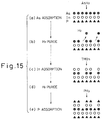
- Fig. 15A illustrates the growth of InPAs, as an example, when the H2 purging time is disadvantageously long.
- ALE P to In to As are grown and if the next H2 purge time is too long, some of already adsorbed As atoms are desorped.
- TMIn is then supplied thereover, In atoms are adsorbed only on the remaining As atoms and not on the already adsorbed In atoms.
- the next H2 purge does not affect the In atoms.
- PH3 is then supplied, P atoms are adsorbed not only on the top In atoms that were adsorbed in the latest step but also on the In atoms on which In atoms were once adsorpted and then desorped.
- a layer of a mixture of As and P is formed and therefore the alloy structure is finally formed.
- Fig. 16A shows the crystal structure of a typical compound semiconductor In GaAs, as an example, grown by the conventional deposition methods.
- the sites of In, Ga and As atoms are random.
- Fig. 16B shows the crystal structure of a compound semiconductor InGaAs, as an example, grown by the ALE process of the present invention.
- the sites of In, Ga and As atoms are in the order of layers and therefore this structure does not cause the carrier scattering by the alloy structure.
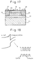
- Fig. 17 shows a high electron mobility transistor (HEMT) in which a non-doped superlattice structure 23 is utilized as an electron channel.
- 21 denotes an Fe-doped semi-insulating InP (1 0 0) substrate
- 22 a non-doped InP buffer layer
- 23 a non-doped (InAs) m (InP) n superlattic structure as an electron channel
- 24 an n-type InP, 25 n+-type contact layers
- 26 a gate electrode
- 27 a source electrode
- 28 a collector electrode.
- Fig. 18 shows the band energy chart of the HEMT as shown in Fig. 17. Since electrons supplied to the channel flow predominantly through the InAs rather than InAs, the (InAs) m (InP) n channel acts almost like an InAs channel, giving a high electron mobility. Further, the periodic structure of the (InAs) m (InP) n is controlled in the atom level by the ALE process of the present invention, the scattering of electrons, particularly by alloying at the interface of the heterojunction, is almost prevented. Generally, dislocation, etc.
- the dislocation can be suppressed by varying the average composition of the channel portion by adequately selecting the m and n of (InAs) m (InP) n .
- a superlattice structure having a unit layer of 20 molecular layers or less, preferably 10 molecular layers or less, more preferably 2 to 5 molecular layers or less can be made, particularly one comprising different In-containing compound semiconductors.
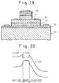
- Fig. 19 shows a heterojunction bipolar transistor (HBT) and Fig. 20 shows the band energy chart of the HBT as shown in Fig. 19.
- HBT heterojunction bipolar transistor
- An emitter 31 is n-type InP ( ⁇ 5 x 1017 cm ⁇ 3) and a collector 32 is n-type InP (1019 ⁇ 1020 cm ⁇ 3), and a base 33 is p-type InAs (1019 ⁇ 1020 cm ⁇ 3 ).
- the interfaces between the base 33 and the emitter 31 and between the base 33 and the collector 3 2 are heterojunctions (double heterojunction structure ).
- 34 denotes a semi-insulating InP substrate, 35 an n+-type In 0.53 Ga 0.47 As contact layer (more than 1019 cm ⁇ 3) and 36 an n+-type In 0.53 Ga 0.47 As contact layer (more than 1019 cm ⁇ 3).
- the switching speed of a bipolar transistor is determined by the time of electron running from the emitter through the base to the neutral portion of the collector, and since the base is made of InAs having a high electron mobility and the band energy chart of Fig. 20 the switching speed of the HBT is very fast.
- This type of electronic device utilizing the high electron mobility of InAs, which has not been manufactured, can be made by utilizing an InAs/InP or the like heterojunction in accordance with the ALE process of the present invention.
Priority Applications (1)
| Application Number | Priority Date | Filing Date | Title |
|---|---|---|---|
| EP01100180A EP1119029A3 (fr) | 1991-07-12 | 1992-07-09 | Epitaxie par couches mono-atomiques d'un semi-conducteur composé |
Applications Claiming Priority (2)
| Application Number | Priority Date | Filing Date | Title |
|---|---|---|---|
| JP17201391 | 1991-07-12 | ||
| JP172013/91 | 1991-07-12 |
Related Child Applications (1)
| Application Number | Title | Priority Date | Filing Date |
|---|---|---|---|
| EP01100180A Division EP1119029A3 (fr) | 1991-07-12 | 1992-07-09 | Epitaxie par couches mono-atomiques d'un semi-conducteur composé |
Publications (2)
| Publication Number | Publication Date |
|---|---|
| EP0523917A2 true EP0523917A2 (fr) | 1993-01-20 |
| EP0523917A3 EP0523917A3 (en) | 1993-09-29 |
Family
ID=15933913
Family Applications (2)
| Application Number | Title | Priority Date | Filing Date |
|---|---|---|---|
| EP01100180A Withdrawn EP1119029A3 (fr) | 1991-07-12 | 1992-07-09 | Epitaxie par couches mono-atomiques d'un semi-conducteur composé |
| EP19920306314 Withdrawn EP0523917A3 (en) | 1991-07-12 | 1992-07-09 | Atomic layer epitaxy of compound semiconductor |
Family Applications Before (1)
| Application Number | Title | Priority Date | Filing Date |
|---|---|---|---|
| EP01100180A Withdrawn EP1119029A3 (fr) | 1991-07-12 | 1992-07-09 | Epitaxie par couches mono-atomiques d'un semi-conducteur composé |
Country Status (2)
| Country | Link |
|---|---|
| US (1) | US5270247A (fr) |
| EP (2) | EP1119029A3 (fr) |
Families Citing this family (92)
| Publication number | Priority date | Publication date | Assignee | Title |
|---|---|---|---|---|
| JP3223575B2 (ja) * | 1992-06-02 | 2001-10-29 | 三菱化学株式会社 | 化合物半導体とその製造方法 |
| JP3137767B2 (ja) * | 1992-10-20 | 2001-02-26 | 富士通株式会社 | 半導体装置の製造方法 |
| JP2605604B2 (ja) * | 1993-11-24 | 1997-04-30 | 日本電気株式会社 | 半導体結晶のエピタキシャル成長方法とそれに用いる分子線供給装置 |
| FI100409B (fi) * | 1994-11-28 | 1997-11-28 | Asm Int | Menetelmä ja laitteisto ohutkalvojen valmistamiseksi |
| US5456206A (en) * | 1994-12-07 | 1995-10-10 | Electronics And Telecommunications Research Institute | Method for two-dimensional epitaxial growth of III-V compound semiconductors |
| US6342277B1 (en) * | 1996-08-16 | 2002-01-29 | Licensee For Microelectronics: Asm America, Inc. | Sequential chemical vapor deposition |
| US5862223A (en) | 1996-07-24 | 1999-01-19 | Walker Asset Management Limited Partnership | Method and apparatus for a cryptographically-assisted commercial network system designed to facilitate and support expert-based commerce |
| US5916365A (en) * | 1996-08-16 | 1999-06-29 | Sherman; Arthur | Sequential chemical vapor deposition |
| KR100265859B1 (ko) * | 1996-12-21 | 2000-09-15 | 정선종 | 전계방출 디스플레이용 발광입자 |
| KR100252049B1 (ko) * | 1997-11-18 | 2000-04-15 | 윤종용 | 원자층 증착법에 의한 알루미늄층의 제조방법 |
| US6511539B1 (en) * | 1999-09-08 | 2003-01-28 | Asm America, Inc. | Apparatus and method for growth of a thin film |
| US6503330B1 (en) | 1999-12-22 | 2003-01-07 | Genus, Inc. | Apparatus and method to achieve continuous interface and ultrathin film during atomic layer deposition |
| US6551399B1 (en) | 2000-01-10 | 2003-04-22 | Genus Inc. | Fully integrated process for MIM capacitors using atomic layer deposition |
| JP3687651B2 (ja) * | 2000-06-08 | 2005-08-24 | ジニテック インク. | 薄膜形成方法 |
| US6620723B1 (en) | 2000-06-27 | 2003-09-16 | Applied Materials, Inc. | Formation of boride barrier layers using chemisorption techniques |
| US7405158B2 (en) | 2000-06-28 | 2008-07-29 | Applied Materials, Inc. | Methods for depositing tungsten layers employing atomic layer deposition techniques |
| US6551929B1 (en) | 2000-06-28 | 2003-04-22 | Applied Materials, Inc. | Bifurcated deposition process for depositing refractory metal layers employing atomic layer deposition and chemical vapor deposition techniques |
| US7101795B1 (en) | 2000-06-28 | 2006-09-05 | Applied Materials, Inc. | Method and apparatus for depositing refractory metal layers employing sequential deposition techniques to form a nucleation layer |
| US7732327B2 (en) | 2000-06-28 | 2010-06-08 | Applied Materials, Inc. | Vapor deposition of tungsten materials |
| US7964505B2 (en) | 2005-01-19 | 2011-06-21 | Applied Materials, Inc. | Atomic layer deposition of tungsten materials |
| US6458416B1 (en) | 2000-07-19 | 2002-10-01 | Micron Technology, Inc. | Deposition methods |
| US7192888B1 (en) | 2000-08-21 | 2007-03-20 | Micron Technology, Inc. | Low selectivity deposition methods |
| US7094690B1 (en) * | 2000-08-31 | 2006-08-22 | Micron Technology, Inc. | Deposition methods and apparatuses providing surface activation |
| US6617173B1 (en) | 2000-10-11 | 2003-09-09 | Genus, Inc. | Integration of ferromagnetic films with ultrathin insulating film using atomic layer deposition |
| US20030190424A1 (en) * | 2000-10-20 | 2003-10-09 | Ofer Sneh | Process for tungsten silicide atomic layer deposition |
| US6355561B1 (en) * | 2000-11-21 | 2002-03-12 | Micron Technology, Inc. | ALD method to improve surface coverage |
| WO2002045871A1 (fr) * | 2000-12-06 | 2002-06-13 | Angstron Systems, Inc. | Systeme et procede de depot module d'une couche atomique induite par des ions |
| US6878402B2 (en) * | 2000-12-06 | 2005-04-12 | Novellus Systems, Inc. | Method and apparatus for improved temperature control in atomic layer deposition |
| US6905547B1 (en) * | 2000-12-21 | 2005-06-14 | Genus, Inc. | Method and apparatus for flexible atomic layer deposition |
| US6998579B2 (en) | 2000-12-29 | 2006-02-14 | Applied Materials, Inc. | Chamber for uniform substrate heating |
| US6825447B2 (en) | 2000-12-29 | 2004-11-30 | Applied Materials, Inc. | Apparatus and method for uniform substrate heating and contaminate collection |
| US6765178B2 (en) | 2000-12-29 | 2004-07-20 | Applied Materials, Inc. | Chamber for uniform substrate heating |
| US20020127336A1 (en) * | 2001-01-16 | 2002-09-12 | Applied Materials, Inc. | Method for growing thin films by catalytic enhancement |
| US6811814B2 (en) | 2001-01-16 | 2004-11-02 | Applied Materials, Inc. | Method for growing thin films by catalytic enhancement |
| US6951804B2 (en) | 2001-02-02 | 2005-10-04 | Applied Materials, Inc. | Formation of a tantalum-nitride layer |
| US6660126B2 (en) | 2001-03-02 | 2003-12-09 | Applied Materials, Inc. | Lid assembly for a processing system to facilitate sequential deposition techniques |
| US6878206B2 (en) | 2001-07-16 | 2005-04-12 | Applied Materials, Inc. | Lid assembly for a processing system to facilitate sequential deposition techniques |
| US6734020B2 (en) | 2001-03-07 | 2004-05-11 | Applied Materials, Inc. | Valve control system for atomic layer deposition chamber |
| US6849545B2 (en) | 2001-06-20 | 2005-02-01 | Applied Materials, Inc. | System and method to form a composite film stack utilizing sequential deposition techniques |
| US7211144B2 (en) | 2001-07-13 | 2007-05-01 | Applied Materials, Inc. | Pulsed nucleation deposition of tungsten layers |
| US7085616B2 (en) | 2001-07-27 | 2006-08-01 | Applied Materials, Inc. | Atomic layer deposition apparatus |
| US7368014B2 (en) * | 2001-08-09 | 2008-05-06 | Micron Technology, Inc. | Variable temperature deposition methods |
| US7049226B2 (en) | 2001-09-26 | 2006-05-23 | Applied Materials, Inc. | Integration of ALD tantalum nitride for copper metallization |
| US6936906B2 (en) | 2001-09-26 | 2005-08-30 | Applied Materials, Inc. | Integration of barrier layer and seed layer |
| US6916398B2 (en) | 2001-10-26 | 2005-07-12 | Applied Materials, Inc. | Gas delivery apparatus and method for atomic layer deposition |
| US6729824B2 (en) | 2001-12-14 | 2004-05-04 | Applied Materials, Inc. | Dual robot processing system |
| US6998014B2 (en) | 2002-01-26 | 2006-02-14 | Applied Materials, Inc. | Apparatus and method for plasma assisted deposition |
| US6911391B2 (en) | 2002-01-26 | 2005-06-28 | Applied Materials, Inc. | Integration of titanium and titanium nitride layers |
| US6827978B2 (en) | 2002-02-11 | 2004-12-07 | Applied Materials, Inc. | Deposition of tungsten films |
| US6833161B2 (en) | 2002-02-26 | 2004-12-21 | Applied Materials, Inc. | Cyclical deposition of tungsten nitride for metal oxide gate electrode |
| US6730367B2 (en) * | 2002-03-05 | 2004-05-04 | Micron Technology, Inc. | Atomic layer deposition method with point of use generated reactive gas species |
| US7439191B2 (en) | 2002-04-05 | 2008-10-21 | Applied Materials, Inc. | Deposition of silicon layers for active matrix liquid crystal display (AMLCD) applications |
| US6846516B2 (en) | 2002-04-08 | 2005-01-25 | Applied Materials, Inc. | Multiple precursor cyclical deposition system |
| US6720027B2 (en) | 2002-04-08 | 2004-04-13 | Applied Materials, Inc. | Cyclical deposition of a variable content titanium silicon nitride layer |
| US6869838B2 (en) | 2002-04-09 | 2005-03-22 | Applied Materials, Inc. | Deposition of passivation layers for active matrix liquid crystal display (AMLCD) applications |
| US6875271B2 (en) | 2002-04-09 | 2005-04-05 | Applied Materials, Inc. | Simultaneous cyclical deposition in different processing regions |
| US7279432B2 (en) | 2002-04-16 | 2007-10-09 | Applied Materials, Inc. | System and method for forming an integrated barrier layer |
| US6825506B2 (en) | 2002-11-27 | 2004-11-30 | Intel Corporation | Field effect transistor and method of fabrication |
| US7262133B2 (en) | 2003-01-07 | 2007-08-28 | Applied Materials, Inc. | Enhancement of copper line reliability using thin ALD tan film to cap the copper line |
| US7211508B2 (en) | 2003-06-18 | 2007-05-01 | Applied Materials, Inc. | Atomic layer deposition of tantalum based barrier materials |
| US7033437B2 (en) * | 2003-06-26 | 2006-04-25 | Rj Mears, Llc | Method for making semiconductor device including band-engineered superlattice |
| US6830964B1 (en) * | 2003-06-26 | 2004-12-14 | Rj Mears, Llc | Method for making semiconductor device including band-engineered superlattice |
| US8993055B2 (en) | 2005-10-27 | 2015-03-31 | Asm International N.V. | Enhanced thin film deposition |
| US8268409B2 (en) * | 2006-10-25 | 2012-09-18 | Asm America, Inc. | Plasma-enhanced deposition of metal carbide films |
| US7611751B2 (en) | 2006-11-01 | 2009-11-03 | Asm America, Inc. | Vapor deposition of metal carbide films |
| US7598170B2 (en) * | 2007-01-26 | 2009-10-06 | Asm America, Inc. | Plasma-enhanced ALD of tantalum nitride films |
| US7595270B2 (en) | 2007-01-26 | 2009-09-29 | Asm America, Inc. | Passivated stoichiometric metal nitride films |
| US7713874B2 (en) * | 2007-05-02 | 2010-05-11 | Asm America, Inc. | Periodic plasma annealing in an ALD-type process |
| KR101308130B1 (ko) * | 2008-03-25 | 2013-09-12 | 서울옵토디바이스주식회사 | 발광 소자 및 그 제조 방법 |
| WO2009129332A2 (fr) | 2008-04-16 | 2009-10-22 | Asm America, Inc. | Dépôt par couche atomique de films de carbure métallique à l'aide de composés hydrocarbure d'aluminium |
| US8383525B2 (en) | 2008-04-25 | 2013-02-26 | Asm America, Inc. | Plasma-enhanced deposition process for forming a metal oxide thin film and related structures |
| US7666474B2 (en) | 2008-05-07 | 2010-02-23 | Asm America, Inc. | Plasma-enhanced pulsed deposition of metal carbide films |
| KR20110133241A (ko) | 2010-06-04 | 2011-12-12 | 서울옵토디바이스주식회사 | 발광 다이오드 제조 방법 |
| US9595438B2 (en) | 2011-09-12 | 2017-03-14 | Nasp Iii/V Gmbh | Method for producing a III/V Si template |
| US9412602B2 (en) | 2013-03-13 | 2016-08-09 | Asm Ip Holding B.V. | Deposition of smooth metal nitride films |
| US8841182B1 (en) | 2013-03-14 | 2014-09-23 | Asm Ip Holding B.V. | Silane and borane treatments for titanium carbide films |
| US8846550B1 (en) | 2013-03-14 | 2014-09-30 | Asm Ip Holding B.V. | Silane or borane treatment of metal thin films |
| US9394609B2 (en) | 2014-02-13 | 2016-07-19 | Asm Ip Holding B.V. | Atomic layer deposition of aluminum fluoride thin films |
| US10643925B2 (en) | 2014-04-17 | 2020-05-05 | Asm Ip Holding B.V. | Fluorine-containing conductive films |
| US10002936B2 (en) | 2014-10-23 | 2018-06-19 | Asm Ip Holding B.V. | Titanium aluminum and tantalum aluminum thin films |
| US9941425B2 (en) | 2015-10-16 | 2018-04-10 | Asm Ip Holdings B.V. | Photoactive devices and materials |
| US9786491B2 (en) | 2015-11-12 | 2017-10-10 | Asm Ip Holding B.V. | Formation of SiOCN thin films |
| US9786492B2 (en) | 2015-11-12 | 2017-10-10 | Asm Ip Holding B.V. | Formation of SiOCN thin films |
| KR102378021B1 (ko) | 2016-05-06 | 2022-03-23 | 에이에스엠 아이피 홀딩 비.브이. | SiOC 박막의 형성 |
| US10186420B2 (en) | 2016-11-29 | 2019-01-22 | Asm Ip Holding B.V. | Formation of silicon-containing thin films |
| US10847529B2 (en) | 2017-04-13 | 2020-11-24 | Asm Ip Holding B.V. | Substrate processing method and device manufactured by the same |
| US10504901B2 (en) | 2017-04-26 | 2019-12-10 | Asm Ip Holding B.V. | Substrate processing method and device manufactured using the same |
| CN110546302B (zh) | 2017-05-05 | 2022-05-27 | Asm Ip 控股有限公司 | 用于受控形成含氧薄膜的等离子体增强沉积方法 |
| US10991573B2 (en) | 2017-12-04 | 2021-04-27 | Asm Ip Holding B.V. | Uniform deposition of SiOC on dielectric and metal surfaces |
| US12359315B2 (en) | 2019-02-14 | 2025-07-15 | Asm Ip Holding B.V. | Deposition of oxides and nitrides |
| US12142479B2 (en) | 2020-01-17 | 2024-11-12 | Asm Ip Holding B.V. | Formation of SiOCN thin films |
| US12341005B2 (en) | 2020-01-17 | 2025-06-24 | Asm Ip Holding B.V. | Formation of SiCN thin films |
Family Cites Families (9)
| Publication number | Priority date | Publication date | Assignee | Title |
|---|---|---|---|---|
| GB2162862B (en) * | 1984-07-26 | 1988-10-19 | Japan Res Dev Corp | A method of growing a thin film single crystalline semiconductor |
| JPH0787179B2 (ja) * | 1984-07-26 | 1995-09-20 | 新技術事業団 | 超格子半導体装置の製造方法 |
| JPS62119196A (ja) * | 1985-11-18 | 1987-05-30 | Univ Nagoya | 化合物半導体の成長方法 |
| JP2587623B2 (ja) * | 1986-11-22 | 1997-03-05 | 新技術事業団 | 化合物半導体のエピタキシヤル結晶成長方法 |
| US4885260A (en) * | 1987-02-17 | 1989-12-05 | Matsushita Electric Industrial Co., Ltd. | Method of laser enhanced vapor phase growth for compound semiconductor |
| JPH0727861B2 (ja) * | 1987-03-27 | 1995-03-29 | 富士通株式会社 | ▲iii▼−▲v▼族化合物半導体結晶の成長方法 |
| JP2736655B2 (ja) * | 1988-06-30 | 1998-04-02 | 富士通株式会社 | 化合物半導体結晶成長方法 |
| JP2647960B2 (ja) * | 1989-05-17 | 1997-08-27 | 日本電子株式会社 | 移動鏡の速度制御装置 |
| JPH042699A (ja) * | 1990-04-18 | 1992-01-07 | Mitsubishi Electric Corp | 結晶成長方法 |
-
1992
- 1992-07-08 US US07/910,766 patent/US5270247A/en not_active Expired - Fee Related
- 1992-07-09 EP EP01100180A patent/EP1119029A3/fr not_active Withdrawn
- 1992-07-09 EP EP19920306314 patent/EP0523917A3/en not_active Withdrawn
Also Published As
| Publication number | Publication date |
|---|---|
| EP1119029A2 (fr) | 2001-07-25 |
| US5270247A (en) | 1993-12-14 |
| EP1119029A3 (fr) | 2001-08-01 |
| EP0523917A3 (en) | 1993-09-29 |
Similar Documents
| Publication | Publication Date | Title |
|---|---|---|
| US5270247A (en) | Atomic layer epitaxy of compound semiconductor | |
| US4767494A (en) | Preparation process of compound semiconductor | |
| US5438952A (en) | Method of growing a semiconductor layer and a fabrication method of a semiconductor device using such a semiconductor layer | |
| US5693139A (en) | Growth of doped semiconductor monolayers | |
| Abernathy | Growth of III–V materials by metalorganic molecular‐beam epitaxy | |
| JPS63240012A (ja) | 3−v族化合物半導体およびその形成方法 | |
| JPH08245291A (ja) | Iii−v族化合物半導体結晶の成長方法 | |
| JPH01290222A (ja) | 半導体気相成長方法 | |
| EP0524817B1 (fr) | Méthode de croissance de cristaux semi-conducteurs d'un compose A-III - B V | |
| US5821155A (en) | Method of growing n-type III-V semiconductor materials on a substrate using SiI4 | |
| JP3159788B2 (ja) | 化合物半導体の結晶成長方法 | |
| JP3223575B2 (ja) | 化合物半導体とその製造方法 | |
| JP3013992B2 (ja) | 化合物半導体結晶の成長方法 | |
| US5296088A (en) | Compound semiconductor crystal growing method | |
| JP2577550B2 (ja) | ▲iii▼−▲v▼族化合物半導体単結晶薄膜の不純物添加法 | |
| KR960004591B1 (ko) | 도우프된 결정 성장 방법 | |
| JP3109149B2 (ja) | 化合物半導体結晶成長方法 | |
| JP3116954B2 (ja) | 化合物半導体薄膜の成長方法 | |
| JPH05190474A (ja) | 化合物半導体の結晶成長方法 | |
| JP3052269B2 (ja) | 気相成長装置およびその成長方法 | |
| JPH0620042B2 (ja) | ▲iii▼−▲v▼族化合物半導体結晶のド−ピング方法 | |
| JP2001210599A (ja) | 化合物半導体の結晶成長方法 | |
| JP2936620B2 (ja) | 化合物半導体結晶の気相成長法 | |
| JPH04279023A (ja) | 3−5族化合物半導体の選択成長方法 | |
| JPH0590160A (ja) | 結晶成長方法 |
Legal Events
| Date | Code | Title | Description |
|---|---|---|---|
| PUAI | Public reference made under article 153(3) epc to a published international application that has entered the european phase |
Free format text: ORIGINAL CODE: 0009012 |
|
| AK | Designated contracting states |
Kind code of ref document: A2 Designated state(s): DE FR GB |
|
| PUAL | Search report despatched |
Free format text: ORIGINAL CODE: 0009013 |
|
| AK | Designated contracting states |
Kind code of ref document: A3 Designated state(s): DE FR GB |
|
| 17P | Request for examination filed |
Effective date: 19940315 |
|
| 17Q | First examination report despatched |
Effective date: 19950622 |
|
| STAA | Information on the status of an ep patent application or granted ep patent |
Free format text: STATUS: THE APPLICATION IS DEEMED TO BE WITHDRAWN |
|
| 18D | Application deemed to be withdrawn |
Effective date: 20010403 |