EP0523952A2 - Gerät zur Aufzeichnung/Wiedergabe von optischem Information- und Aufzeichnungsmedium - Google Patents
Gerät zur Aufzeichnung/Wiedergabe von optischem Information- und Aufzeichnungsmedium Download PDFInfo
- Publication number
- EP0523952A2 EP0523952A2 EP92306423A EP92306423A EP0523952A2 EP 0523952 A2 EP0523952 A2 EP 0523952A2 EP 92306423 A EP92306423 A EP 92306423A EP 92306423 A EP92306423 A EP 92306423A EP 0523952 A2 EP0523952 A2 EP 0523952A2
- Authority
- EP
- European Patent Office
- Prior art keywords
- data
- information recording
- elements
- reproducing apparatus
- read
- Prior art date
- Legal status (The legal status is an assumption and is not a legal conclusion. Google has not performed a legal analysis and makes no representation as to the accuracy of the status listed.)
- Granted
Links
Images


Classifications
-
- G—PHYSICS
- G11—INFORMATION STORAGE
- G11B—INFORMATION STORAGE BASED ON RELATIVE MOVEMENT BETWEEN RECORD CARRIER AND TRANSDUCER
- G11B20/00—Signal processing not specific to the method of recording or reproducing; Circuits therefor
- G11B20/10—Digital recording or reproducing
- G11B20/18—Error detection or correction; Testing, e.g. of drop-outs
-
- G—PHYSICS
- G11—INFORMATION STORAGE
- G11B—INFORMATION STORAGE BASED ON RELATIVE MOVEMENT BETWEEN RECORD CARRIER AND TRANSDUCER
- G11B20/00—Signal processing not specific to the method of recording or reproducing; Circuits therefor
- G11B20/10—Digital recording or reproducing
- G11B20/10009—Improvement or modification of read or write signals
-
- G—PHYSICS
- G11—INFORMATION STORAGE
- G11B—INFORMATION STORAGE BASED ON RELATIVE MOVEMENT BETWEEN RECORD CARRIER AND TRANSDUCER
- G11B20/00—Signal processing not specific to the method of recording or reproducing; Circuits therefor
- G11B20/10—Digital recording or reproducing
- G11B20/18—Error detection or correction; Testing, e.g. of drop-outs
- G11B20/1816—Testing
- G11B20/182—Testing using test patterns
-
- G—PHYSICS
- G11—INFORMATION STORAGE
- G11B—INFORMATION STORAGE BASED ON RELATIVE MOVEMENT BETWEEN RECORD CARRIER AND TRANSDUCER
- G11B27/00—Editing; Indexing; Addressing; Timing or synchronising; Monitoring; Measuring tape travel
- G11B27/36—Monitoring, i.e. supervising the progress of recording or reproducing
-
- G—PHYSICS
- G11—INFORMATION STORAGE
- G11B—INFORMATION STORAGE BASED ON RELATIVE MOVEMENT BETWEEN RECORD CARRIER AND TRANSDUCER
- G11B7/00—Recording or reproducing by optical means, e.g. recording using a thermal beam of optical radiation by modifying optical properties or the physical structure, reproducing using an optical beam at lower power by sensing optical properties; Record carriers therefor
- G11B7/004—Recording, reproducing or erasing methods; Read, write or erase circuits therefor
- G11B7/005—Reproducing
-
- G—PHYSICS
- G11—INFORMATION STORAGE
- G11B—INFORMATION STORAGE BASED ON RELATIVE MOVEMENT BETWEEN RECORD CARRIER AND TRANSDUCER
- G11B20/00—Signal processing not specific to the method of recording or reproducing; Circuits therefor
- G11B20/10—Digital recording or reproducing
- G11B20/18—Error detection or correction; Testing, e.g. of drop-outs
- G11B20/1816—Testing
- G11B2020/183—Testing wherein at least one additional attempt is made to read or write the data when a first attempt is unsuccessful
Definitions
- the present invention generally relates to an optical information recording and reproducing apparatus for recording and reproducing information on an optical disk having optically detectable guide tracks and more particularly, to an optical information recording and reproducing apparatus in which a processing for recovering data errors at the time of reproduction of signals recorded on the optical disk is performed.
- raw error rate of the optical disks ranges from 10 ⁇ 4 to 10 ⁇ 6 which is quite higher than that of 10 ⁇ 9 to 10 ⁇ 12 obtained in magnetic disks representative of known recording mediums.
- optical information recording and reproducing apparatuses employing optical disks have powerful error control and a verification function that immediately after data has been recorded at a track, contents recorded at the track are reproduced such that it is verified whether the data has been recorded at the track correctly.
- verification function verification is performed at the time of recording of the data. If it is found that the data is recorded at a defective sector referred to above and thus, contents of the data cannot be guaranteed, the data is rerecorded at an alternative sector provided at another location preliminarily.
- the prior art reproduction signal processing circuit includes an optical disk 1, a motor 2 for rotating the optical disk 1, an optical head 3 which condenses to a light beam having a diameter of about 1 ⁇ m, a laser beam emitted from a semiconductor laser or the like so as to irradiate the light beam over the optical disk 1 and a laser drive circuit 4 for modulating and driving the semiconductor laser, etc. in response to a recording information signal inputted to a terminal A.
- the known reproduction signal processing circuit further includes a pre-amplifier 42 for amplifying weak signals from the optical disk 1, a frequency characteristics correcting circuit 43 for emphasizing a specific frequency so as to facilitate reading of the data, a differentiating circuit 7, an amplifier 8, a zero-cross comparator 9, an AND gate 15, a phase locked loop (PLL) circuit 46, an address/data reading circuit 16 and a microprocessor 63 for controlling recording signals and reproduction signals or controlling the known information recording and reproducing apparatus as a whole.
- the known reproduction signal processing circuit includes first and second envelope detecting circuits 44 and 12 for detecting an envelope of a signal, first and second comparators 11 and 14 and a bias setting circuit 45 for setting a bias of the second comparator 14.
- a reproduction signal read by the optical head 3 is amplified by the pre-amplifier 42. Frequency characteristics of the reproduction signal amplified by the pre-amplifier 42 are corrected by the frequency characteristics correcting circuit 43.
- Fig. 7(a) shows one example of an output signal of the frequency characteristics correcting circuit 43. Peak detection of the reproduction signal is performed by two circuitries. One of the circuitries is a system for detecting peak of the reproduction signal and is constituted by the differentiating circuit 7, the amplifier 8 and the zero-cross comparator 9. An output signal of the differentiating circuit 7 is shown in Fig. (b), while an output signal of the zero-cross comparator 9 is shown in Fig. (c) such that data is carried at a rise edge of the output signal of the zero-cross comparator 9. A crossed portion in Fig. 7(c) represents a noise signal.
- the other of the circuitry is a data gate detecting system for eliminating the noise signal referred to above and is constituted by the first envelope detecting circuit 44 and the first comparator 11.
- an output signal of the first envelope detecting circuit 44 is usually set such that about 40 % of amplitude of the input signal is clipped.
- an output signal of the first comparator 11 is obtained as shown in Fig. 7(d) and peak of the data is detected by logical product of Figs. 7(c) and 7(d) as shown in Fig. 7(e).
- output of the data is performed by a gate signal of a data detecting circuit for detecting presence and absence of of the data such that the data is outputted to only a sector which is regarded as recording the data therein.
- the data detecting circuit is formed by the second envelope detecting circuit 12, the bias setting circuit 45 and the second comparator 14.
- An output of the second comparator 13 is obtained as shown in Fig. 7(f) and finally, an output of the AND gate 15 is obtained as the reproduction signal as shown in Fig. 7(g).
- this binary signal is read by the address/data reading circuit 16 and any error is detected by the address/data reading circuit 16 during or after reading of the data, the address/data reading circuit 16 feeds error information back to the microprocessor 63.
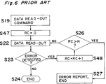
- Fig. 6 is a flow chart showing processing at the time of read-out of the data in the known information recording and reproducing apparatus.
- the program flow proceeds in the sequence of steps S19, step S47, step S22, step S23 and step S24.
- step S19 a data read-out command is received, while at step S47, a retry counter RC is initialized.
- step S22 the data is read out, while at step S23, it is judged whether or not an error has been detected.
- the program flow ends at step S24.
- the program flow proceeds in the sequence of steps S19, S47, S22, S23, S48, S26, S22, S23, S48, S26, ---, S48, S26, S22, S23 and S24.
- step S48 an increment is imparted to count of the retry counter RC.
- step S26 it is judged whether or not the count of the retry counter RC has exceeded a retry number N.
- Fig. 8(a) shows an output signal of the frequency characteristics correcting circuit 43 of Fig. 5. Character a in Fig. 8(a) shows an output signal of the first envelope detecting circuit 44, while Fig.
- FIG. 8(d) shows a gate signal for detecting peak.
- Fig. 8(b) shows an output signal of the differentiating circuit 7
- Fig. 8(c) shows an output signal of the zero-cross comparator 9. Accordingly, peak of the data is detected by logical product of Figs. 8(c) and 8(d) and thus, a portion of the unerased signals is detected erroneously as shown in Fig. 8(e).
- a gate signal for detecting presence and absence of the data is shown in Fig. 8(f), while an output signal of the AND gate 15 also has a portion of the unerased signals as shown in Fig. 8(g). In this case, a data error is produced.
- step S27 follows. As described above, such a case may take place that data in a sector having, e.g., many unerased signals is correctly read by verification of one optical disk drive but is detected by another optical disk drive as containing a data error.
- an object of an embodiment of the present invention is to provide, with a view to eliminating the disadvantages inherent in conventional information recording and reproducing apparatuses, an optical information recording and reproducing apparatus in which in case a data error is detected during or after reading of data, the data is read a plurality of times by changing a plurality of variable parameters of a reproduction signal processing circuit so as to raise reliability of the recorded data.
- An optical information recording and reproducing apparatus comprises a reproduction signal processing circuit including one or more elements having respective variable parameters such that a microprocessor acting as a detection means for detecting a data error can set the parameters by utilizing an output from an analog switch or a digital-analog converter. Meanwhile, when a data error is detected during read-out of the data, the parameters are reset before rereading, in addition to the,known procedures.
- a value minimizing an error in read-out of the data, which has been determined by the detection means, is selected for each of the parameters so as to be recorded at a specific location of the optical disk such that conditional setting in the subsequent read-out is accurately performed immediately.
- the reproduction signal processing circuit includes an optical disk 1, a motor 2 for rotating the optical disk 1, an optical head 3 which condenses to a light beam having a diameter of about 1 ⁇ m, a laser beam emitted from a semiconductor laser or the like so as to irradiate the light beam over the optical disk 1, a laser drive circuit 4 for modulating and driving the semiconductor laser, etc.
- a differentiating circuit 7 in response to a recording information signal inputted to a terminal A, a differentiating circuit 7, an amplifier 8, a zero-cross comparator 9, an AND gate 15, an address/data reading circuit 16, a second envelope detecting circuit 12 for detecting an envelope of a signal and first and second comparators 11 and 14.
- the production signal processing circuit of Fig. 1 further includes a microprocessor 17 which detects read-out errors of addresses and data from the address/data reading circuit 16 and is capable of setting a plurality of variable parameters of the production signal processing circuit, a pre-amplifier 5 in which amplification degree can be variably set by the microprocessor 17, a frequency characteristics correcting circuit 6 in which characteristics of frequency correction can be variably set by the microprocessor 17, a first envelope detecting circuit 10 in which comparison level for the first comparator 11 can be variably set by the microprocessor 17, a bias setting circuit 13 for setting a bias of the second comparator 14, in which voltage level can be variably set by the microprocessor 17 and a phase locked loop (PLL) circuit 18 which fetches data synchronously with a binary data signal at fetching timing variably set by the microprocessor 17.
- PLL phase locked loop
- microprocessor 17, pre-amplifier 5, frequency characteristics correcting circuit 6, first envelope detecting circuit 10, bias setting circuit 13 and PLL circuit 18 correspond to but are different, in function, from the microprocessor 63, the pre-amplifier 42, the frequency characteristics correcting circuit 43, the first envelope detecting circuit 44, the bias setting circuit 45 and the PLL circuit 46 of the prior art production signal processing circuit of Fig. 5, respectively.
- Fig. 3(a) shows an output signal of the frequency characteristics correcting circuit 6.
- the parameter of the first envelope detecting circuit 10 is set to, for example, about 40 % of amplitude of an input signal, the output signal of the frequency characteristics correcting circuit 6 is obtained as shown by the portion a in Fig. 3(a) and thus, a portion of the unerased signals is detected erroneously.
- An output signal of the first comparator 11 is shown in Fig. 3(d), while an output signal of the differentiating circuit 7 is shown in Fig. 3(b). Since an output signal of the zero-cross comparator 9 also detects the unerased signals, an output of the AND gate 15 also detects a portion of the unerased signals. An output signal of the AND gate 15 is shown in Fig. 3(g). A data error is produced in the address/data reading circuit 16 and is detected by the microprocessor 17.
- the microprocessor 17 which has detected the data error performs a preparation for rereading the data in accordance with a flow chart of Fig. 2.
- the program flow proceeds in the sequence of steps S19, S20, S21, S22, S23, S25, S26 and S21.
- a data read-out command is received, while at step S20, a retry counter RC and a parameter control counter PCC are initialized.
- parameters of the production signal processing circuit are set, while at step S22, data read-out is executed.
- step S23 it is judged whether or not an error has been detected.
- an increment is imparted to counts of the retry counter RC and the parameter control counter PCC.
- step S26 it is judged whether or not the count of the retry counter RC has exceeded a retry number N.
- the microprocessor 17 sets, for example, the parameter of the frequency characteristics correcting circuit 6 gentler by reducing lead amount of a lead compensating circuit and restricting a high-frequency component and sets the parameter of the first envelope detecting circuit 10 to, e.g., about 65 % of amplitude of an input signal.
- an output signal of the frequency characteristics correcting circuit 6 is obtained as shown in Fig..4(a). Since the parameter of the first envelope detecting circuit 10 is set to about 65 % of amplitude of the input signal, the output signal of the frequency characteristics correcting circuit 6 is shown by the portion a in Fig.
- read-out of the data is further repeated by changing the above parameters. Then, when an error is detected in the read data even if reading is repeated a predetermined reading number of N times, error processing is performed.
- the frequency characteristics correcting circuit 6 can be formed by two or more sets of leading capacitors and resistors and an analog switch for effecting changeover among the sets. If a digital-analog converter is employed, levels of the first envelope detecting circuit 10 and the bias setting circuit 13 can be directly changed by changing data in the microprocessor 17. Alternatively, a plurality of biases may also be prepared so as to be changed over by using an analog switch. Amplification degree of the pre-amplifier 5 can be changed by employing a programmable amplifier or changing over a feedback resistance of an amplifier by an analog switch.
- phase of the PLL circuit 18 can be changed easily by adding an output of the digital-analog converter to the phase at a fixed gain after a phase comparator in the PLL circuit 18. Since each of these procedures represents one example, it is needless to say that the parameters can be changed by employing other procedures.
- the parameters of the reproduction signal processing circuit which are converted into predetermined codes and are set initially, may be determined by reading a track in a variable parameter region 1P (Fig. 10(a)) of the optical disk 1 and then, the data is read out.
- the parameters are sequentially changed in accordance with setting of the parameter control counter PCC. Conditions minimizing the errors are written at the track in the variable parameter region 1P of the optical disk 1.
- read-out is performed on the basis of this information written at the track in the variable parameter region 1P.
- Figs. 10(a) and 10(b) show the optical disk 1.
- the optical disk 1 includes a user region 1U disposed at its radially outermost portion and the variable parameter region 1P disposed radially inwardly of the user region 1U.
- the variable parameter region 1P stores addresses D11 and D21, PCC data D12 and drive identification data D13.
- the addresses D11 and D21 include addresses indicative of radial positions of tracks on the optical disk 1 and sector information indicative of angular positions of the tracks on the optical disk 1 and are preliminarily recorded on the optical disk 1 in embossed shape such as intermissions, etc. of the tracks.
- the PCC data D12 is data of the parameter control counter PCC.
- the PCC data D12 may be recorded in a fixed sequence for each of the parameters or information which determines combination of each of the parameters by a specific code may be recorded.
- the drive identification data D13 may be separate identification information for drives or may also be group identification information indicative of levels of model change, etc. When the drive identification data D13 is recorded and is used together with the PCC data D12 as necessary, the data read-out conditions can be determined more accurately and more promptly.
- the embodiment is applied to the optical disk having many unerased signals. It has been confirmed that data errors produced in damaged or repeatedly used optical disks can be corrected by setting different parameters, respectively. Therefore, by setting parameters corresponding to the respective signal deterioration factors at the time of rereading of the data in accordance with one embodiment of the present invention, reliability of read-out of the data can be improved remarkably.
- the optical disk is described.
- the present invention since the present invention is directed to an apparatus for processing recorded signals, the present invention can also be widely applied to a device for recording and reproducing signals optically such as an optical card, an optical tape or the like and an apparatus for recording signals magnetically.
- the data is reread a plurality of times by changing a plurality of the set parameters of the production signal processing circuit such that reliability of recording and reproduction of the data can be raised. Meanwhile, if these conditions are written at a specific location of the optical disk and read-out is performed on the basis of this written information when the data is reproduced next time, the medians of the parameters associated with the optical disk can be determined immediately and thus, highly reliable data read-out conditions can be determined promptly.
- the program flow ends at the normal end routine for the data which could be read in rereading.
Landscapes
- Engineering & Computer Science (AREA)
- Signal Processing (AREA)
- Optical Recording Or Reproduction (AREA)
Applications Claiming Priority (2)
| Application Number | Priority Date | Filing Date | Title |
|---|---|---|---|
| JP17369991 | 1991-07-15 | ||
| JP173699/91 | 1991-07-15 |
Publications (3)
| Publication Number | Publication Date |
|---|---|
| EP0523952A2 true EP0523952A2 (de) | 1993-01-20 |
| EP0523952A3 EP0523952A3 (en) | 1993-12-01 |
| EP0523952B1 EP0523952B1 (de) | 1999-06-02 |
Family
ID=15965486
Family Applications (1)
| Application Number | Title | Priority Date | Filing Date |
|---|---|---|---|
| EP92306423A Expired - Lifetime EP0523952B1 (de) | 1991-07-15 | 1992-07-14 | Gerät zur Aufzeichnung/Wiedergabe von optischem Information- und Aufzeichnungsmedium |
Country Status (4)
| Country | Link |
|---|---|
| US (1) | US5600616A (de) |
| EP (1) | EP0523952B1 (de) |
| CA (1) | CA2073804C (de) |
| DE (1) | DE69229304T2 (de) |
Cited By (1)
| Publication number | Priority date | Publication date | Assignee | Title |
|---|---|---|---|---|
| EP0994477A1 (de) * | 1998-10-14 | 2000-04-19 | Sony Corporation | Plattenantrieb zum Wiederlesen desselben Signals einer Platte im Falle eines Lesesignalfehlers |
Families Citing this family (3)
| Publication number | Priority date | Publication date | Assignee | Title |
|---|---|---|---|---|
| US5424881A (en) | 1993-02-01 | 1995-06-13 | Cirrus Logic, Inc. | Synchronous read channel |
| JP3702817B2 (ja) * | 2000-09-13 | 2005-10-05 | ティアック株式会社 | 光ディスクドライブ装置 |
| JP2009087464A (ja) * | 2007-09-28 | 2009-04-23 | Toshiba Corp | 光ディスク装置およびトラッキング制御方法 |
Family Cites Families (14)
| Publication number | Priority date | Publication date | Assignee | Title |
|---|---|---|---|---|
| FR2301133A1 (fr) * | 1975-02-14 | 1976-09-10 | Thomson Csf | Dispo |
| JPS60175111A (ja) * | 1984-02-20 | 1985-09-09 | Fanuc Ltd | ロボツト制御装置 |
| JPS6419565A (en) * | 1987-07-13 | 1989-01-23 | Canon Kk | Information recording and reproducing device |
| JPH01107377A (ja) * | 1987-10-20 | 1989-04-25 | Nec Corp | 光記憶装置 |
| JP2513747B2 (ja) * | 1987-12-17 | 1996-07-03 | パイオニア株式会社 | デ―タ記録再生方法 |
| JP2554719B2 (ja) * | 1988-09-30 | 1996-11-13 | 株式会社東芝 | 記録データ読取り方式 |
| JPH02128325A (ja) * | 1988-11-08 | 1990-05-16 | Fujitsu Ltd | 光学的記憶装置 |
| JPH02166670A (ja) * | 1988-12-20 | 1990-06-27 | Tokico Ltd | 磁気ディスク装置 |
| DE69030962T2 (de) * | 1989-03-13 | 1998-01-02 | Sony Corp | Automatischer Entzerrer |
| JPH02265025A (ja) * | 1989-04-05 | 1990-10-29 | Pioneer Electron Corp | サーボループのループゲイン設定方法 |
| JP2667522B2 (ja) * | 1989-07-06 | 1997-10-27 | 株式会社日立製作所 | 光ディスク装置 |
| JPH0430331A (ja) * | 1990-05-24 | 1992-02-03 | Matsushita Electric Ind Co Ltd | 光記録情報のリードベリファイ方法、ならびにリードベリファイ用再生回路 |
| JP3282180B2 (ja) * | 1990-08-28 | 2002-05-13 | ソニー株式会社 | 磁気記録再生装置 |
| US5136569A (en) * | 1990-09-28 | 1992-08-04 | International Business Machines Corporation | Optical disk recorder for diverse media types and having a predetermined initialization or start-up procedure |
-
1992
- 1992-07-14 CA CA002073804A patent/CA2073804C/en not_active Expired - Fee Related
- 1992-07-14 DE DE69229304T patent/DE69229304T2/de not_active Expired - Fee Related
- 1992-07-14 EP EP92306423A patent/EP0523952B1/de not_active Expired - Lifetime
-
1994
- 1994-04-06 US US08/224,099 patent/US5600616A/en not_active Expired - Fee Related
Cited By (2)
| Publication number | Priority date | Publication date | Assignee | Title |
|---|---|---|---|---|
| EP0994477A1 (de) * | 1998-10-14 | 2000-04-19 | Sony Corporation | Plattenantrieb zum Wiederlesen desselben Signals einer Platte im Falle eines Lesesignalfehlers |
| US6545832B1 (en) | 1998-10-14 | 2003-04-08 | Alps Electric Co., Ltd. | Disk drive capable of rereading same signal from disk in case of error in read signal |
Also Published As
| Publication number | Publication date |
|---|---|
| CA2073804C (en) | 1998-12-22 |
| DE69229304T2 (de) | 2000-02-24 |
| EP0523952A3 (en) | 1993-12-01 |
| US5600616A (en) | 1997-02-04 |
| CA2073804A1 (en) | 1993-01-16 |
| DE69229304D1 (de) | 1999-07-08 |
| EP0523952B1 (de) | 1999-06-02 |
Similar Documents
| Publication | Publication Date | Title |
|---|---|---|
| US4774700A (en) | Information recording and reproducing apparatus with detection and management of defective sectors | |
| US4881136A (en) | Method and apparatus for detecting minute defects on magnetic disk by monitoring both amplitude decrease and phase shift of a reproduced signal | |
| US5218590A (en) | Optical disk apparatus having improved recording capacity | |
| US5724325A (en) | Method for reducing lead in time in an optical disk recording or reproducing apparatus capable of processing data for multiple types of disks | |
| US5777964A (en) | Optical disk apparatus | |
| JPS6358672A (ja) | 情報処理装置 | |
| HK41496A (en) | Method of and device for adjusting recording parameters | |
| US6839193B2 (en) | Method and apparatus for determining read-to-write head offset of a disk drive | |
| EP0523952B1 (de) | Gerät zur Aufzeichnung/Wiedergabe von optischem Information- und Aufzeichnungsmedium | |
| JP2529192B2 (ja) | 情報記録再生方法 | |
| JP3264385B2 (ja) | 光デイスク記録再生装置 | |
| US5999506A (en) | Data recording/reproducing device and recording medium | |
| US5748590A (en) | Apparatus for inspecting disc recording medium | |
| JP2882189B2 (ja) | 光情報記録再生装置 | |
| US5153866A (en) | Optical disc recording-reproducing apparatus for determining the last recorded sensor | |
| JP2809479B2 (ja) | データ記録再生装置 | |
| JPH03116566A (ja) | 光磁気ディスク記録再生制御方法 | |
| US5023876A (en) | Method and apparatus for detecting finally recorded sector | |
| JP3250244B2 (ja) | トラックジャンプ制御装置 | |
| JPS60121575A (ja) | 光学的情報記録再生装置 | |
| JP2568528B2 (ja) | 信号記録再生装置 | |
| JPH10188316A (ja) | ディスク装置およびその記録パワーのキャリブレーション方法 | |
| JPH0772942B2 (ja) | 光デイスク装置 | |
| JPH06259769A (ja) | 光学式情報記録再生装置における記録パワー値設定方法 | |
| KR100564615B1 (ko) | 광 디스크 기록 방법 및 장치 |
Legal Events
| Date | Code | Title | Description |
|---|---|---|---|
| PUAI | Public reference made under article 153(3) epc to a published international application that has entered the european phase |
Free format text: ORIGINAL CODE: 0009012 |
|
| 17P | Request for examination filed |
Effective date: 19920724 |
|
| AK | Designated contracting states |
Kind code of ref document: A2 Designated state(s): DE FR GB |
|
| PUAL | Search report despatched |
Free format text: ORIGINAL CODE: 0009013 |
|
| AK | Designated contracting states |
Kind code of ref document: A3 Designated state(s): DE FR GB |
|
| 17Q | First examination report despatched |
Effective date: 19951219 |
|
| GRAG | Despatch of communication of intention to grant |
Free format text: ORIGINAL CODE: EPIDOS AGRA |
|
| GRAG | Despatch of communication of intention to grant |
Free format text: ORIGINAL CODE: EPIDOS AGRA |
|
| GRAH | Despatch of communication of intention to grant a patent |
Free format text: ORIGINAL CODE: EPIDOS IGRA |
|
| GRAH | Despatch of communication of intention to grant a patent |
Free format text: ORIGINAL CODE: EPIDOS IGRA |
|
| GRAA | (expected) grant |
Free format text: ORIGINAL CODE: 0009210 |
|
| AK | Designated contracting states |
Kind code of ref document: B1 Designated state(s): DE FR GB |
|
| REF | Corresponds to: |
Ref document number: 69229304 Country of ref document: DE Date of ref document: 19990708 |
|
| ET | Fr: translation filed | ||
| PLBE | No opposition filed within time limit |
Free format text: ORIGINAL CODE: 0009261 |
|
| STAA | Information on the status of an ep patent application or granted ep patent |
Free format text: STATUS: NO OPPOSITION FILED WITHIN TIME LIMIT |
|
| 26N | No opposition filed | ||
| REG | Reference to a national code |
Ref country code: GB Ref legal event code: IF02 |
|
| PGFP | Annual fee paid to national office [announced via postgrant information from national office to epo] |
Ref country code: DE Payment date: 20050707 Year of fee payment: 14 |
|
| PGFP | Annual fee paid to national office [announced via postgrant information from national office to epo] |
Ref country code: FR Payment date: 20050708 Year of fee payment: 14 |
|
| PGFP | Annual fee paid to national office [announced via postgrant information from national office to epo] |
Ref country code: GB Payment date: 20050713 Year of fee payment: 14 |
|
| PG25 | Lapsed in a contracting state [announced via postgrant information from national office to epo] |
Ref country code: GB Free format text: LAPSE BECAUSE OF NON-PAYMENT OF DUE FEES Effective date: 20060714 |
|
| PG25 | Lapsed in a contracting state [announced via postgrant information from national office to epo] |
Ref country code: DE Free format text: LAPSE BECAUSE OF NON-PAYMENT OF DUE FEES Effective date: 20070201 |
|
| GBPC | Gb: european patent ceased through non-payment of renewal fee |
Effective date: 20060714 |
|
| REG | Reference to a national code |
Ref country code: FR Ref legal event code: ST Effective date: 20070330 |
|
| PG25 | Lapsed in a contracting state [announced via postgrant information from national office to epo] |
Ref country code: FR Free format text: LAPSE BECAUSE OF NON-PAYMENT OF DUE FEES Effective date: 20060731 |