EP0524724A2 - Protection de dispositifs à circuit intégré - Google Patents
Protection de dispositifs à circuit intégré Download PDFInfo
- Publication number
- EP0524724A2 EP0524724A2 EP92305552A EP92305552A EP0524724A2 EP 0524724 A2 EP0524724 A2 EP 0524724A2 EP 92305552 A EP92305552 A EP 92305552A EP 92305552 A EP92305552 A EP 92305552A EP 0524724 A2 EP0524724 A2 EP 0524724A2
- Authority
- EP
- European Patent Office
- Prior art keywords
- capacitance
- switch means
- power supply
- circuit according
- supply lines
- Prior art date
- Legal status (The legal status is an assumption and is not a legal conclusion. Google has not performed a legal analysis and makes no representation as to the accuracy of the status listed.)
- Withdrawn
Links
Images
Classifications
-
- H—ELECTRICITY
- H10—SEMICONDUCTOR DEVICES; ELECTRIC SOLID-STATE DEVICES NOT OTHERWISE PROVIDED FOR
- H10W—GENERIC PACKAGES, INTERCONNECTIONS, CONNECTORS OR OTHER CONSTRUCTIONAL DETAILS OF DEVICES COVERED BY CLASS H10
- H10W42/00—Arrangements for protection of devices
- H10W42/20—Arrangements for protection of devices protecting against electromagnetic or particle radiation, e.g. light, X-rays, gamma-rays or electrons
-
- H—ELECTRICITY
- H02—GENERATION; CONVERSION OR DISTRIBUTION OF ELECTRIC POWER
- H02H—EMERGENCY PROTECTIVE CIRCUIT ARRANGEMENTS
- H02H5/00—Emergency protective circuit arrangements for automatic disconnection directly responsive to an undesired change from normal non-electric working conditions with or without subsequent reconnection
- H02H5/005—Emergency protective circuit arrangements for automatic disconnection directly responsive to an undesired change from normal non-electric working conditions with or without subsequent reconnection responsive to ionising radiation; Nuclear-radiation circumvention circuits
-
- H—ELECTRICITY
- H03—ELECTRONIC CIRCUITRY
- H03K—PULSE TECHNIQUE
- H03K19/00—Logic circuits, i.e. having at least two inputs acting on one output; Inverting circuits
- H03K19/003—Modifications for increasing the reliability for protection
- H03K19/0033—Radiation hardening
-
- Y—GENERAL TAGGING OF NEW TECHNOLOGICAL DEVELOPMENTS; GENERAL TAGGING OF CROSS-SECTIONAL TECHNOLOGIES SPANNING OVER SEVERAL SECTIONS OF THE IPC; TECHNICAL SUBJECTS COVERED BY FORMER USPC CROSS-REFERENCE ART COLLECTIONS [XRACs] AND DIGESTS
- Y10—TECHNICAL SUBJECTS COVERED BY FORMER USPC
- Y10S—TECHNICAL SUBJECTS COVERED BY FORMER USPC CROSS-REFERENCE ART COLLECTIONS [XRACs] AND DIGESTS
- Y10S257/00—Active solid-state devices, e.g. transistors, solid-state diodes
- Y10S257/921—Radiation hardened semiconductor device
Definitions
- This invention relates to the protection of integrated circuit (IC) devices against latch-up during a nuclear event.
- a conventional method of preventing such latch-up is to arrange for the power supply of an equipment incorporating IC devices susceptible to such latch-up to be temporarily grounded via a so-called crow-bar switch which is closed in response to detection of a nuclear event by a detector specifically provided for the detection of such events.
- Such a method has the disadvantages that the crow-bar switch has to become very rapidly capable of passing a large current and that the supply is interrupted not only to IC devices which require gamma induced latch-up protection, but also to other devices of an equipment.
- a circuit comprising at least one integrated circuit device; a pair of power supply lines for said device; a capacitance connected across said power supply lines which serves to reduce transients in the power supplied via said lines to said device in normal operation of the circuit; and connected across said capacitance a switch means whose impedance when a transient gamma pulse is incident thereon during a nuclear event is reduced to a low value at a rate such that the energy stored in the capacitance is discharged through the switch means and the voltage applied to the device via the power supply lines is pulled down to such a level and at such a rate as to prevent transient gamma pulse induced latch-up in the device.
- the capacitance is constituted substantially wholly by the inherent capacitance arising from the structure of the switch means, but in other arrangements the capacitance is constituted partly by the inherent capacitance of the switch means and partly by a capacitor connected in parallel therewith.
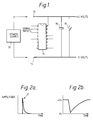
- the circuit essentially comprises: an integrated circuit (IC) device 11 connected between power supply lines 13; a capacitance 15 connected between the lines 13; and a switch means 17 connected in parallel with the capacitance 15.
- IC integrated circuit
- the capacitance 15 is of such a value that when lines 13 are connected to a power supply 19, the energy stored by the capacitance 15 is sufficient to supply necessary operating currents to the IC device 11 during its normal operation.
- the capacitance 15 is of sufficiently high value to prevent significant transients appearing in the voltage supply to the IC device 11 in normal operation.
- the switch means 17 is so constructed that under a transient gamma pulse P incident thereon during a nuclear event, its impedance is set to a low value whereby the energy stored by the capacitance 15 is rapidly discharged through the switch means 17.
- the low impedance of the switch means is, moreover, such and the rate at which the low impedance of the switch means 15 is attained is such that the voltage applied to the lines 13 is pulled down to such a level and at such a rate as to prevent transient gamma pulse induced latch-up in the IC device 11.
- FIGS 2 a and 2 b illustrate the gamma pulse P and the required consequent effect of the impedance drop of switch means 17 on the voltage across the capacitance 15 and hence the power lines 13.
- IC devices not shown
- FIG. 2 a and 2 b illustrate the gamma pulse P and the required consequent effect of the impedance drop of switch means 17 on the voltage across the capacitance 15 and hence the power lines 13.
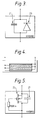
- the switch means 17 is conveniently a semiconductor device such as a PIN diode. Typically such a diode, in its common implementations, will have a chip, i.e. inherent, capacitance of 320pf. Experiment has shown, however, that for transient suppression a capacitance of around 2000pF or more is called for. Accordingly the capacitance 15 and switch means 17 typically comprise a hybrid device, referred to for convenience as an active capacitor, comprising a capacitor 21 and a PIN diode 23 as shown in Figure 3.
- an active capacitor in the form of a PIN diode stack comprising a multiplicity of PIN diodes as shown in Figure 4 is used providing not only the gamma pulse response necessary but possessing an inherent capacitance of the requisite value e.g. 2000pF or more.
- An additional separate capacitor as shown in Figure 3 is then not required.
- a switch means 17 other than a PIN diode may of course be employed, as shown in Figure 5 where the switch means 17 is constituted by a MOS-FET device 25.
- the overall arrangement must be such that: the supply lines 13 are reduced to a low, e.g. ground potential; the speed of operation is sufficiently high to prevent latch-up; and the circuit, in particular the capacitance 15 and switch means 17, are able to survive a multiplicity of gamma pulses i.e. still maintain functionality after a nuclear event has occurred.
Landscapes
- Physics & Mathematics (AREA)
- High Energy & Nuclear Physics (AREA)
- Engineering & Computer Science (AREA)
- Computer Hardware Design (AREA)
- Computing Systems (AREA)
- General Engineering & Computer Science (AREA)
- Mathematical Physics (AREA)
- Semiconductor Integrated Circuits (AREA)
Applications Claiming Priority (2)
| Application Number | Priority Date | Filing Date | Title |
|---|---|---|---|
| GB9115976A GB9115976D0 (en) | 1991-07-24 | 1991-07-24 | Protection of integrated circuit devices |
| GB9115976 | 1991-07-24 |
Publications (2)
| Publication Number | Publication Date |
|---|---|
| EP0524724A2 true EP0524724A2 (fr) | 1993-01-27 |
| EP0524724A3 EP0524724A3 (en) | 1993-03-31 |
Family
ID=10698896
Family Applications (1)
| Application Number | Title | Priority Date | Filing Date |
|---|---|---|---|
| EP19920305552 Withdrawn EP0524724A3 (en) | 1991-07-24 | 1992-06-17 | Protection of integrated circuit devices |
Country Status (3)
| Country | Link |
|---|---|
| US (1) | US5391931A (fr) |
| EP (1) | EP0524724A3 (fr) |
| GB (1) | GB9115976D0 (fr) |
Cited By (3)
| Publication number | Priority date | Publication date | Assignee | Title |
|---|---|---|---|---|
| GB2619295A (en) * | 2022-05-30 | 2023-12-06 | Energy Res Lab Ltd | EMP protection system |
| GB2624359A (en) * | 2022-06-13 | 2024-05-22 | Energy Res Lab Ltd | Grid protection apparatus and method |
| EP4377995A1 (fr) * | 2021-07-30 | 2024-06-05 | Airbus Defence and Space SAS | Système électronique spatial |
Families Citing this family (4)
| Publication number | Priority date | Publication date | Assignee | Title |
|---|---|---|---|---|
| US5672918A (en) * | 1994-08-18 | 1997-09-30 | The United States Of America As Represented By The United States Department Of Energy | System level latchup mitigation for single event and transient radiation effects on electronics |
| US20050134323A1 (en) * | 2003-12-23 | 2005-06-23 | Honeywell International Inc. | Single event transient filter for comparator |
| US7322015B2 (en) * | 2005-01-05 | 2008-01-22 | Honeywell Internatinal Inc. | Simulating a dose rate event in a circuit design |
| US7858425B2 (en) * | 2007-05-21 | 2010-12-28 | Sanders Thomas J | Monolithic nuclear event detector and method of manufacture |
Family Cites Families (14)
| Publication number | Priority date | Publication date | Assignee | Title |
|---|---|---|---|---|
| US3886379A (en) * | 1972-12-13 | 1975-05-27 | Motorola Inc | Radiation triggered disconnect means |
| US3982197A (en) * | 1974-02-04 | 1976-09-21 | Rca Corporation | Radiation responsive voltage dividing circuit |
| US4010403A (en) * | 1974-06-27 | 1977-03-01 | Gte Sylvania Incorporated | Radiation protected solid state voltage regulating apparatus |
| US4037140A (en) * | 1976-04-14 | 1977-07-19 | Rca Corporation | Protection circuit for insulated-gate field-effect transistors (IGFETS) |
| GB2136648B (en) * | 1983-03-01 | 1986-05-14 | Plessey Co Plc | Trigger circuit |
| GB2136222A (en) * | 1983-03-01 | 1984-09-12 | Plessey Co Plc | Switched mode power supplies |
| US4687622A (en) * | 1985-10-29 | 1987-08-18 | Irt Corporation | Nuclear event detector |
| GB8621839D0 (en) * | 1986-09-10 | 1986-10-15 | British Aerospace | Electrostatic discharge protection circuit |
| US4800299A (en) * | 1986-12-18 | 1989-01-24 | Northrop Corporation | Method and apparatus for MOSFET radiation failure circumvention |
| IT1217104B (it) * | 1987-03-03 | 1990-03-14 | Sgs Microelettronica Spa | Circuito integrato cmos a due alimentazioni con un transistore mos integrato di protezione contro il <<latch-up>>. |
| US4794261A (en) * | 1987-04-24 | 1988-12-27 | General Electric Company | Radiation protection circuit for protection against gamma ray and neutron radiation |
| GB8823398D0 (en) * | 1988-10-05 | 1989-05-17 | Marconi Gec Ltd | Nuclear event detectors |
| US5103283A (en) * | 1989-01-17 | 1992-04-07 | Hite Larry R | Packaged integrated circuit with in-cavity decoupling capacitors |
| GB2241798B (en) * | 1990-03-06 | 1994-01-12 | Plessey Co Ltd | Radiation hardened power supplies for integrated circuits |
-
1991
- 1991-07-24 GB GB9115976A patent/GB9115976D0/en active Pending
-
1992
- 1992-06-17 EP EP19920305552 patent/EP0524724A3/en not_active Withdrawn
- 1992-06-22 US US07/901,832 patent/US5391931A/en not_active Expired - Fee Related
Cited By (5)
| Publication number | Priority date | Publication date | Assignee | Title |
|---|---|---|---|---|
| EP4377995A1 (fr) * | 2021-07-30 | 2024-06-05 | Airbus Defence and Space SAS | Système électronique spatial |
| EP4377995B1 (fr) * | 2021-07-30 | 2025-10-08 | Airbus Defence and Space SAS | Sytème électronique pour applications spatiales |
| GB2619295A (en) * | 2022-05-30 | 2023-12-06 | Energy Res Lab Ltd | EMP protection system |
| GB2619295B (en) * | 2022-05-30 | 2024-07-03 | Energy Res Lab Ltd | EMP protection system |
| GB2624359A (en) * | 2022-06-13 | 2024-05-22 | Energy Res Lab Ltd | Grid protection apparatus and method |
Also Published As
| Publication number | Publication date |
|---|---|
| EP0524724A3 (en) | 1993-03-31 |
| GB9115976D0 (en) | 1991-11-06 |
| US5391931A (en) | 1995-02-21 |
Similar Documents
| Publication | Publication Date | Title |
|---|---|---|
| US5959820A (en) | Cascode LVTSCR and ESD protection circuit | |
| US5463520A (en) | Electrostatic discharge protection with hysteresis trigger circuit | |
| US5255146A (en) | Electrostatic discharge detection and clamp control circuit | |
| US5721656A (en) | Electrostatc discharge protection network | |
| US6353520B1 (en) | Shared 5 volt tolerant ESD protection circuit for low voltage CMOS process | |
| US5617283A (en) | Self-referencing modulation circuit for CMOS integrated circuit electrostatic discharge protection clamps | |
| US5754381A (en) | Output ESD protection with high-current-triggered lateral SCR | |
| US3725739A (en) | Dual mode power supply protection circuit | |
| US5917689A (en) | General purpose EOS/ESD protection circuit for bipolar-CMOS and CMOS integrated circuits | |
| US5751525A (en) | EOS/ESD Protection circuit for an integrated circuit with operating/test voltages exceeding power supply rail voltages | |
| EP1277236A1 (fr) | Circuit de protection contre la decharge electrostatique (esd) | |
| US5550699A (en) | Hot plug tolerant ESD protection for an IC | |
| US5124877A (en) | Structure for providing electrostatic discharge protection | |
| US5010321A (en) | Nuclear event detectors | |
| WO2001045173A1 (fr) | Structure de diode esd amelioree | |
| US5644460A (en) | Multi-rail electrostatic discharge protection device | |
| US4321644A (en) | Power line transient limiter | |
| US5391931A (en) | Protection of integrated circuit devices | |
| KR100249162B1 (ko) | 정전기(eds)보호회로 | |
| WO1997015975A1 (fr) | Protection contre les decharges electrostatiques pour des circuits d'entree/sortie tolerant les surtensions | |
| US5892262A (en) | Capacitor-triggered electrostatic discharge protection circuit | |
| EP0528668B1 (fr) | Protection de semi-conducteurs contre les transitoires à haute énergie | |
| JP5159057B2 (ja) | 静電放電パワークランプ内での過渡事象効果を低減するための方法及びシステム | |
| EP1911093A2 (fr) | Protection contre les decharges electrostatiques (des) haute tension avec chemin partage au moyen de dispositifs de calage basse tension repartis | |
| US20040130368A1 (en) | Circuit for providing resistance to single event upset to pulse width modulator integrated circuit |
Legal Events
| Date | Code | Title | Description |
|---|---|---|---|
| PUAI | Public reference made under article 153(3) epc to a published international application that has entered the european phase |
Free format text: ORIGINAL CODE: 0009012 |
|
| AK | Designated contracting states |
Kind code of ref document: A2 Designated state(s): DE ES FR GB IT |
|
| PUAL | Search report despatched |
Free format text: ORIGINAL CODE: 0009013 |
|
| AK | Designated contracting states |
Kind code of ref document: A3 Designated state(s): DE ES FR GB IT |
|
| 17P | Request for examination filed |
Effective date: 19930914 |
|
| 17Q | First examination report despatched |
Effective date: 19950809 |
|
| STAA | Information on the status of an ep patent application or granted ep patent |
Free format text: STATUS: THE APPLICATION IS DEEMED TO BE WITHDRAWN |
|
| 18D | Application deemed to be withdrawn |
Effective date: 19951220 |