EP0524741A1 - Verfahren zur Erhöhung der Bildauflösung einer Maske für die Herstellung von Halbleiterschaltungen - Google Patents
Verfahren zur Erhöhung der Bildauflösung einer Maske für die Herstellung von Halbleiterschaltungen Download PDFInfo
- Publication number
- EP0524741A1 EP0524741A1 EP92306211A EP92306211A EP0524741A1 EP 0524741 A1 EP0524741 A1 EP 0524741A1 EP 92306211 A EP92306211 A EP 92306211A EP 92306211 A EP92306211 A EP 92306211A EP 0524741 A1 EP0524741 A1 EP 0524741A1
- Authority
- EP
- European Patent Office
- Prior art keywords
- phase shift
- mask
- layer
- forming
- region
- Prior art date
- Legal status (The legal status is an assumption and is not a legal conclusion. Google has not performed a legal analysis and makes no representation as to the accuracy of the status listed.)
- Withdrawn
Links
- 239000004065 semiconductor Substances 0.000 title claims abstract description 23
- 238000000034 method Methods 0.000 title claims description 23
- 230000010363 phase shift Effects 0.000 claims abstract description 130
- 239000011248 coating agent Substances 0.000 claims abstract description 15
- 238000000576 coating method Methods 0.000 claims abstract description 15
- VYPSYNLAJGMNEJ-UHFFFAOYSA-N Silicium dioxide Chemical compound O=[Si]=O VYPSYNLAJGMNEJ-UHFFFAOYSA-N 0.000 claims description 10
- VYZAMTAEIAYCRO-UHFFFAOYSA-N Chromium Chemical compound [Cr] VYZAMTAEIAYCRO-UHFFFAOYSA-N 0.000 claims description 9
- 229910052581 Si3N4 Inorganic materials 0.000 claims description 6
- HQVNEWCFYHHQES-UHFFFAOYSA-N silicon nitride Chemical compound N12[Si]34N5[Si]62N3[Si]51N64 HQVNEWCFYHHQES-UHFFFAOYSA-N 0.000 claims description 6
- 235000012239 silicon dioxide Nutrition 0.000 claims description 5
- 239000000377 silicon dioxide Substances 0.000 claims description 5
- 238000005229 chemical vapour deposition Methods 0.000 claims description 3
- 238000000623 plasma-assisted chemical vapour deposition Methods 0.000 claims description 3
- XUIMIQQOPSSXEZ-UHFFFAOYSA-N Silicon Chemical compound [Si] XUIMIQQOPSSXEZ-UHFFFAOYSA-N 0.000 claims description 2
- 229910052710 silicon Inorganic materials 0.000 claims description 2
- 239000010703 silicon Substances 0.000 claims description 2
- 238000004519 manufacturing process Methods 0.000 abstract description 4
- 239000000463 material Substances 0.000 description 27
- 238000005530 etching Methods 0.000 description 9
- 239000010408 film Substances 0.000 description 9
- 239000000758 substrate Substances 0.000 description 9
- 238000000151 deposition Methods 0.000 description 5
- 230000000873 masking effect Effects 0.000 description 5
- 230000008021 deposition Effects 0.000 description 4
- 239000011521 glass Substances 0.000 description 3
- 229920002120 photoresistant polymer Polymers 0.000 description 3
- IJGRMHOSHXDMSA-UHFFFAOYSA-N Atomic nitrogen Chemical compound N#N IJGRMHOSHXDMSA-UHFFFAOYSA-N 0.000 description 2
- 230000007547 defect Effects 0.000 description 2
- 230000001788 irregular Effects 0.000 description 2
- 238000004544 sputter deposition Methods 0.000 description 2
- 229910020781 SixOy Inorganic materials 0.000 description 1
- VZPPHXVFMVZRTE-UHFFFAOYSA-N [Kr]F Chemical compound [Kr]F VZPPHXVFMVZRTE-UHFFFAOYSA-N 0.000 description 1
- 239000006117 anti-reflective coating Substances 0.000 description 1
- ISQINHMJILFLAQ-UHFFFAOYSA-N argon hydrofluoride Chemical compound F.[Ar] ISQINHMJILFLAQ-UHFFFAOYSA-N 0.000 description 1
- QVGXLLKOCUKJST-UHFFFAOYSA-N atomic oxygen Chemical compound [O] QVGXLLKOCUKJST-UHFFFAOYSA-N 0.000 description 1
- 230000002238 attenuated effect Effects 0.000 description 1
- 230000015572 biosynthetic process Effects 0.000 description 1
- 230000001427 coherent effect Effects 0.000 description 1
- 238000009826 distribution Methods 0.000 description 1
- AMGQUBHHOARCQH-UHFFFAOYSA-N indium;oxotin Chemical compound [In].[Sn]=O AMGQUBHHOARCQH-UHFFFAOYSA-N 0.000 description 1
- 229910052757 nitrogen Inorganic materials 0.000 description 1
- 230000003287 optical effect Effects 0.000 description 1
- 239000001301 oxygen Substances 0.000 description 1
- 229910052760 oxygen Inorganic materials 0.000 description 1
- 238000002310 reflectometry Methods 0.000 description 1
- 238000001228 spectrum Methods 0.000 description 1
- 238000007736 thin film deposition technique Methods 0.000 description 1
Images


Classifications
-
- G—PHYSICS
- G03—PHOTOGRAPHY; CINEMATOGRAPHY; ANALOGOUS TECHNIQUES USING WAVES OTHER THAN OPTICAL WAVES; ELECTROGRAPHY; HOLOGRAPHY
- G03F—PHOTOMECHANICAL PRODUCTION OF TEXTURED OR PATTERNED SURFACES, e.g. FOR PRINTING, FOR PROCESSING OF SEMICONDUCTOR DEVICES; MATERIALS THEREFOR; ORIGINALS THEREFOR; APPARATUS SPECIALLY ADAPTED THEREFOR
- G03F1/00—Originals for photomechanical production of textured or patterned surfaces, e.g., masks, photo-masks, reticles; Mask blanks or pellicles therefor; Containers specially adapted therefor; Preparation thereof
- G03F1/26—Phase shift masks [PSM]; PSM blanks; Preparation thereof
- G03F1/29—Rim PSM or outrigger PSM; Preparation thereof
Definitions
- the present invention relates, in general, to masks used in manufacturing semiconductors, and more particularly, to a novel phase shift mask.
- phase shift mask included phase shift elements that shifted the phase of a portion of light that passed through the mask's apertures. thereby producing a smaller light pattern.
- phase shift elements One disadvantage of previous phase shift masks was the phase shift elements that were required. Forming the phase shift elements generally involved covering the mask with a phase shift material, applying a mask to define the phase shift elements, and etching away unwanted portions of the phase shift material. Since the phase shift elements were smaller than the apertures, this new mask had to be carefully aligned to the apertures. The additional deposition, masking, and etching operations not only added additional manufacturing cost, but could also create defects in the phase shift material and in the mask.
- phase shift elements Another disadvantage was the difficulty in determining the pattern to be used to create the phase shift elements. In general, only a portion of the apertures received phase shift elements. Consequently, complicated mask generation algorithms were required to determine the placement of the phase shift elements. Often the algorithm did not result in optimum element placement and the result was a minimal improvement in the resolution provided by a conventional mask.
- phase shift mask that does not have individual phase shift elements, that does not require additional masking and etching operations, that has a phase shift region that is self-aligned to mask apertures, and that has a phase region thickness that is independent of the phase shift material's thickness.
- the present invention provides a phase shift mask that can be used for manufacturing semiconductors.
- the mask has a pattern layer that contains the predetermined pattern of a desired semiconductor feature which is formed in a plurality of apertures in the pattern layer.
- a conformal coating is applied to the mask in order to form a phase shift region within a predetermined distance of each aperture.
- the conformal coating forms two regions having different thicknesses. The phase of light passing through the thicker or phase shift region is shifted relative to light passing through the thin region.
- the word(s) "light”, either single or plural, mean(s) electromagnetic waves that may be coherent or incoherent and that have wavelengths that may be in the visible or other spectrums.
- FIG. 1 illustrates a cross-sectional view of a portion of a conventional semiconductor mask 10 to which phase shift elements will be added in accordance to the prior art.
- Mask 10 includes a pattern layer 12 which contains a predetermined pattern of a desired semiconductor device feature.
- a glass substrate 11 provides support for a thin layer of chrome that typically is used to create pattern layer 12.
- an anti-reflective coating 13 is applied to pattern 12 to reduce reflections from the chrome.
- Pattern layer 12 includes a plurality of apertures, such as apertures 14, 16, and 17, through which light passes to form an illuminated pattern in the shape of the desired semiconductor device feature.
- indium tin oxide is typically used to create a transparent film 15 that covers a conventional mask such as mask 10 of FIG. 1.
- Transparent film 15 is generally applied by sputtering or other similar techniques.
- the resulting film 15 has an irregular surface that matches the elevations and openings of pattern layer 12.
- Masking and etching operations will transform portions of transparent film 15 that are within apertures 14, 16, and 17 into phase shift elements.
- a photo resist layer is applied to film 15 and formed into an etch mask 35.
- a pattern for exposing the photo resist layer is formed by modifying the pattern used to form pattern layer 12. Generally, each element and shape of pattern layer 12 is enlarged by some amount to form the pattern for etch mask 35.
- FIG. 3 is the prior art mask of FIG. 2 after the etching operation has been completed and etch mask 35 has been removed.
- the portions of film 15 that remain in apertures 14, 16, and 17 form phase shift elements.
- the irregular shape of film layer 15 near the top corners of pattern layer 12 result from the non-uniform deposition, e.g. sputtering, of film layer 15 as discussed in FIG. 2.
- FIG. 4 illustrates a cross sectional portion of a phase shift mask 24 that is suitable for producing fine geometry semiconductor devices in accordance with the present invention.
- Phase shift mask 24 includes a rigid transparent substrate 25 on which a pattern layer 26 has been formed.
- a plurality of apertures in pattern layer 26 form a predetermined pattern that is suitable for use in forming a desired semiconductor device feature.
- a low reflectivity layer (not shown) may cover pattern layer 26.
- substrate 25 is glass while pattern layer 26 is a layer of chrome.
- the glass used for substrate 25, the chrome used for pattern layer 26, and the methods of forming pattern layer 26 on substrate 25 are similar to the techniques used to form conventional mask 10 shown in FIG. 1.
- Phase shift mask 24 also includes a phase shift layer 27 that covers pattern layer 26 and exposed portions of substrate 25, and has a thickness 28.
- Phase shift layer 27 is a conformal coating of a material that is applied using conformal thin film deposition methods such as chemical vapor deposition (CVD), plasma enhanced chemical vapor deposition (PECVD), or other similar conformal deposition methods.
- the material used for phase shift layer 27 has an index of refraction suitable for producing a 180° phase shift as light passes through the material.
- the phase shift is created by passing light through two different thicknesses of phase shift layer 27.
- a thin or reference region 32 functions as a reference that permits light to pass through without a phase shift.
- a thick or phase shift region 31 has a greater thickness than reference region 32.
- phase shift region 31 and reference region 32 are highlighted by dashed lines.
- the difference in thickness between region 31 and region 32 creates a 180° difference in the phase of light that passes through regions 31 and 32. This thickness difference is formed by the conformal characteristics of the coating that is used for phase shift layer 27.
- the thickness of phase shift region 31 is equal to thickness 28 of phase shift layer 27 plus the thickness of pattern layer 26, while the thickness of reference region 32 is equal to thickness 28.
- the difference in thickness between phase shift region 31 and reference region 32 is the thickness of pattern layer 26, and is referred to as a phase shift thickness 33. Therefore phase shift thickness 33 is determined by the thickness of pattern layer 26 and is independent from thickness 28 of phase shift layer 27.
- phase shift layer 27 results in a coating that closely reproduces the topology of the conventional mask to which phase shift layer 27 is applied. These conformal characteristics provides phase shift region 31 with a shape that closely matches the sidewalls of pattern layer 26 and has a clear delineation near the top edges of pattern layer 26. This is an improvement compared to the prior phase shift elements of prior phase shift masks as shown in FIG. 3. Because phase shift layer 27 is a conformal coating, phase shift layer 27 has thickness 28 on exposed portions of substrate 25, on pattern layer 26, and on the sidewalls of pattern layer 26. Consequently, phase shift region 31 has a width 29 that is equal to thickness 28, and is independent from phase shift thickness 33.
- phase shift region 31 is a significant improvement over prior methods of forming a phase shift mask.
- forming phase shift region 31 with a single conformal deposition that does not require mask alignments or etching is a further improvement over previous methods of forming phase shift masks.
- phase shift mask 24 the distance (d) is equal to phase shift thickness 33.
- the index of refraction (n) is the index of refraction of the material used for phase shift layer 27.
- phase shift layer 27 is silicon nitride (Si3N4) which has an index of refraction of approximately 2.05. It is important to note that the phase shift equation is independent from thickness 28 of phase shift layer 27. Consequently, the thickness of pattern layer 26 can be varied to provide a value for phase shift thickness 33 that is suitable for a particular wavelength of light and a particular index of refraction, while thickness 28 of phase shift layer 27 can be varied for a desired width 29 of phase shift region 31. Width 29 is typically determined by the smallest aperture on a phase shift mask.
- phase shift layer materials are illustrated hereinafter in FIG. 6.
- FIG. 5 is a graph illustrating a light intensity pattern that is produced as light passes through the apertures of phase shift mask 24 that is shown in FIG. 4. Since the graph of FIG. 5 is produced by light transmitted through phase shift mask 24 of FIG. 4, the discussion of FIG. 5 will have references to FIG. 4.
- the ordinate of FIG. 5 represents the phase and intensity of light that is transmitted through mask 24, and the abscissa represents position relative to mask 24.
- An in-phase graph 39 represents the distribution of light that is transmitted through a reference region 34 of phase shift mask 24. As light passes through region 34, the light is bent in the area near the corners of pattern layer 26 and is formed into a diffraction pattern as shown by graph 39.
- the intensity of graph 39 has at least two maximas 48 that reduce the resolution of light passing through region 34.
- Light passing through a phase shift region 36 and a phase shift region 37 travels a further distance through the material of regions 36 and 37.
- the light intensity pattern is attenuated in addition to being shifted 180° as indicated by a graph 41 and a graph 42.
- Graph 41 results from light passing through phase shift region 36
- graph 42 results from passing through phase shift region 37.
- the downward excursion of graphs 41 and 42 indicates that a 180° phase shift has occurred.
- the light that produces graphs 41 and 42 is 180° out of phase with the light that produces graph 39, therefore, the light patterns algebraically add together and produce an interference pattern as illustrated by a corresponding portion of a dashed line 46.
- phase shift mask 24 produces a much sharper image and higher resolution than a corresponding conventional mask, and can be manufactured from a conventional mask without additional masking and etching operations.
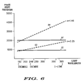
- FIG. 6 is a graph illustrating pattern layer thicknesses that are required for some phase shift layer materials at various wavelengths of light.
- the abscissa represents light wavelength in nanometers, while the ordinate represents pattern layer or phase shift thickness in angstroms. Also included on the abscissa is the light wavelength emitted by three semiconductor mask exposure systems.
- An I-line exposure system generally has an emission at a wavelength of 365 nanometers
- a krypton fluoride (KrF) Excimer I laser has an emission at approximately 248 nanometers
- an argon fluoride (ArF) Excimer II laser system generally emits light having a wavelength of approximately 193 nanometers.
- FIG. 6 provides an easy method to compare the refraction index of phase shift layer materials, to optical system wavelengths and pattern layer thickness.
- the examples of FIG. 6 illustrate some material combinations that can be utilized to produce a phase shift mask from a conventional semiconductor mask. Other materials and thicknesses can be used for the pattern layer, and other materials can be used for the phase shift layer.
- chrome is the generally accepted pattern layer material in the semiconductor industry and the currently accepted thickness for such chrome layers is between approximately 900 angstroms and 2000 angstroms, these thicknesses are represented in FIG. 6 by a graph 51 and a graph 52, respectively.
- the phase shift thicknesses (d) required to provide a 180° phase shift are calculated, using the equation of FIG. 4, and the values plotted on the graph of FIG. 6. If the calculated phase shift thickness lies between graphs 51 and 52, a chrome pattern layer of that thickness can be created to provide the desired phase shift layer.
- a graph 53 illustrates an example of such a calculated pattern layer or phase shift thicknesses for a silicon nitride phase shift layer which has an index of refraction of approximately 2.05. Since graph 53 lies between graphs 51 and 52, a chrome pattern layer thickness can be formed for each of the wavelengths shown in FIG. 6. Therefore, silicon nitride can be used as a phase shift layer material for all of the wavelengths shown in FIG. 6.
- a graph 54 illustrates similar phase shift thicknesses that are required for a silicon dioxide (SiO2) phase shift layer that has an index of refraction of approximately 1.46. Graph 54 indicates that the particular conditions of the example shown in FIG. 6 limit the use of SiO2 as a phase shift layer to wavelengths below approximately 200 nanometers.
- silicon oxynitride Si x O y N z
- the pattern layer thickness for such materials can be calculated from the equation of FIG. 4 in a similar manner.
- phase shift mask Covering the pattern layer and substrate of a conventional mask with a conformal coating creates a versatile phase shift layer.
- the phase shift region thickness that is required to establish the phase shift is independent from the width of the phase shift region.
- Use of the conformal phase shift layer permits forming a phase shift mask from a conventional mask with a single deposition of a conformal coating.
- the phase shift region along with the reference region is created without additional etching or masking operations, consequently, no additional mask defects are created while forming the phase shift mask. No complicated algorithms are required to determine a phase shift mask pattern, consequently, the method easily fits into conventional mask making procedures and is compatible with conventional mask making equipment.
Landscapes
- Physics & Mathematics (AREA)
- General Physics & Mathematics (AREA)
- Preparing Plates And Mask In Photomechanical Process (AREA)
- Exposure And Positioning Against Photoresist Photosensitive Materials (AREA)
- Exposure Of Semiconductors, Excluding Electron Or Ion Beam Exposure (AREA)
Applications Claiming Priority (2)
| Application Number | Priority Date | Filing Date | Title |
|---|---|---|---|
| US72925991A | 1991-07-12 | 1991-07-12 | |
| US729259 | 1991-07-12 |
Publications (1)
| Publication Number | Publication Date |
|---|---|
| EP0524741A1 true EP0524741A1 (de) | 1993-01-27 |
Family
ID=24930254
Family Applications (1)
| Application Number | Title | Priority Date | Filing Date |
|---|---|---|---|
| EP92306211A Withdrawn EP0524741A1 (de) | 1991-07-12 | 1992-07-07 | Verfahren zur Erhöhung der Bildauflösung einer Maske für die Herstellung von Halbleiterschaltungen |
Country Status (2)
| Country | Link |
|---|---|
| EP (1) | EP0524741A1 (de) |
| JP (1) | JPH05197129A (de) |
Cited By (2)
| Publication number | Priority date | Publication date | Assignee | Title |
|---|---|---|---|---|
| WO1994019723A1 (en) * | 1993-02-23 | 1994-09-01 | Interuniversitair Micro-Elektronica | Resolution-enhancing optical phase structure for a projection illumination system |
| EP0660185A3 (de) * | 1993-12-23 | 1996-07-17 | Ibm | Vereinfachtes Verfahren zur Herstellung von Phasenverschiebungsmasken mit Randstruktur. |
Citations (6)
| Publication number | Priority date | Publication date | Assignee | Title |
|---|---|---|---|---|
| JPH02140743A (ja) * | 1988-11-22 | 1990-05-30 | Hitachi Ltd | 集積回路装置の製造方法 |
| EP0401795A2 (de) * | 1989-06-08 | 1990-12-12 | Oki Electric Industry Company, Limited | Phasenverschiebungs-Photomaske für negative Lacke und Verfahren zur Herstellung von isolierten negativen Resistbildern mit dieser Phasenverschiebungsmaske |
| JPH03237458A (ja) * | 1990-02-14 | 1991-10-23 | Mitsubishi Electric Corp | 微細パターン形成方法 |
| EP0453310A1 (de) * | 1990-04-19 | 1991-10-23 | Sharp Kabushiki Kaisha | Maske für Photolithographie |
| EP0475694A2 (de) * | 1990-09-10 | 1992-03-18 | Fujitsu Limited | Optische Phasenmaske und Verfahren zur Herstellung |
| EP0489540A2 (de) * | 1990-12-05 | 1992-06-10 | AT&T Corp. | Lithographische Phasenverschiebungsmasken mit erhöhter Auflösung |
-
1992
- 1992-07-07 EP EP92306211A patent/EP0524741A1/de not_active Withdrawn
- 1992-07-10 JP JP20625192A patent/JPH05197129A/ja active Pending
Patent Citations (8)
| Publication number | Priority date | Publication date | Assignee | Title |
|---|---|---|---|---|
| JPH02140743A (ja) * | 1988-11-22 | 1990-05-30 | Hitachi Ltd | 集積回路装置の製造方法 |
| US5045417A (en) * | 1988-11-22 | 1991-09-03 | Hitachi, Ltd. | Mask for manufacturing semiconductor device and method of manufacture thereof |
| EP0401795A2 (de) * | 1989-06-08 | 1990-12-12 | Oki Electric Industry Company, Limited | Phasenverschiebungs-Photomaske für negative Lacke und Verfahren zur Herstellung von isolierten negativen Resistbildern mit dieser Phasenverschiebungsmaske |
| JPH03237458A (ja) * | 1990-02-14 | 1991-10-23 | Mitsubishi Electric Corp | 微細パターン形成方法 |
| EP0453310A1 (de) * | 1990-04-19 | 1991-10-23 | Sharp Kabushiki Kaisha | Maske für Photolithographie |
| JPH043412A (ja) * | 1990-04-19 | 1992-01-08 | Sharp Corp | 光露光用マスク及びその製造方法 |
| EP0475694A2 (de) * | 1990-09-10 | 1992-03-18 | Fujitsu Limited | Optische Phasenmaske und Verfahren zur Herstellung |
| EP0489540A2 (de) * | 1990-12-05 | 1992-06-10 | AT&T Corp. | Lithographische Phasenverschiebungsmasken mit erhöhter Auflösung |
Non-Patent Citations (3)
| Title |
|---|
| PATENT ABSTRACTS OF JAPAN vol. 014, no. 814 (P-1092)14 August 1990 & JP-A-02 140 743 ( HITACHI LTD ) 30 May 1990 * |
| PATENT ABSTRACTS OF JAPAN vol. 016, no. 019 (P-1300)17 January 1992 & JP-A-03 237 458 ( MITSUBISHI ELECTRIC CORP ) 23 October 1991 * |
| PATENT ABSTRACTS OF JAPAN vol. 016, no. 146 (E-1188)10 April 1992 & JP-A-04 003 412 ( SHARP CORP ) 8 January 1992 * |
Cited By (3)
| Publication number | Priority date | Publication date | Assignee | Title |
|---|---|---|---|---|
| WO1994019723A1 (en) * | 1993-02-23 | 1994-09-01 | Interuniversitair Micro-Elektronica | Resolution-enhancing optical phase structure for a projection illumination system |
| US5624773A (en) * | 1993-02-23 | 1997-04-29 | Interuniversitair Micro-Elektronica Centrum Vzw | Resolution-enhancing optical phase structure for a projection illumination system |
| EP0660185A3 (de) * | 1993-12-23 | 1996-07-17 | Ibm | Vereinfachtes Verfahren zur Herstellung von Phasenverschiebungsmasken mit Randstruktur. |
Also Published As
| Publication number | Publication date |
|---|---|
| JPH05197129A (ja) | 1993-08-06 |
Similar Documents
| Publication | Publication Date | Title |
|---|---|---|
| US6306547B1 (en) | Photomask and manufacturing method thereof, and exposure method using the photomask | |
| US5358808A (en) | Exposure mask, method of manufacturing the same, and exposure method using the same | |
| US5354632A (en) | Lithography using a phase-shifting reticle with reduced transmittance | |
| US5677111A (en) | Process for production of micropattern utilizing antireflection film | |
| EP0453310B1 (de) | Maske für Photolithographie | |
| US5424153A (en) | Optical mask using phase shift and method of producing the same | |
| US5902493A (en) | Method for forming micro patterns of semiconductor devices | |
| US5840447A (en) | Multi-phase photo mask using sub-wavelength structures | |
| US5382483A (en) | Self-aligned phase-shifting mask | |
| US5484672A (en) | Method of making a rim-type phase-shift mask | |
| US5292623A (en) | Method for forming integrated circuit devices using a phase shifting mask | |
| KR100213250B1 (ko) | 위상 쉬프트 마스크 및 그 제조방법 | |
| US5300378A (en) | Method of producing a phase shifting mask | |
| JP3478067B2 (ja) | ハーフトーン型位相シフトマスク及びハーフトーン型位相シフトマスク用ブランク | |
| US5567552A (en) | Method for fabricating a phase shift mask | |
| US5635335A (en) | Method for fabricating semiconductor device utilizing dual photoresist films imaged with same exposure mask | |
| KR20020087986A (ko) | 위상시프트 마스크의 제조 방법 및 위상시프트 마스크 | |
| US5468576A (en) | Method for manufacturing exposure mask | |
| US5356738A (en) | Reticle comprising phase shifter with a tapered edge | |
| US5547813A (en) | Method of forming a fine resist pattern of high resolution using a contrast enhancement layer | |
| JPH05197129A (ja) | 半導体製造用位相シフトマスク | |
| KR0144942B1 (ko) | 패턴 형성방법, 이에 사용되는 마스크 및 그 제조방법 | |
| US6350547B1 (en) | Oxide structure having a finely calibrated thickness | |
| KR19990050484A (ko) | 하프-톤 위상 반전 마스크의 제조 방법 | |
| EP0490320A2 (de) | Verfahren zur Herstellung eines Beugungsgitters |
Legal Events
| Date | Code | Title | Description |
|---|---|---|---|
| PUAI | Public reference made under article 153(3) epc to a published international application that has entered the european phase |
Free format text: ORIGINAL CODE: 0009012 |
|
| AK | Designated contracting states |
Kind code of ref document: A1 Designated state(s): DE FR GB IT |
|
| STAA | Information on the status of an ep patent application or granted ep patent |
Free format text: STATUS: THE APPLICATION IS DEEMED TO BE WITHDRAWN |
|
| 18D | Application deemed to be withdrawn |
Effective date: 19930728 |