EP0453310B1 - Maske für Photolithographie - Google Patents
Maske für Photolithographie Download PDFInfo
- Publication number
- EP0453310B1 EP0453310B1 EP91303545A EP91303545A EP0453310B1 EP 0453310 B1 EP0453310 B1 EP 0453310B1 EP 91303545 A EP91303545 A EP 91303545A EP 91303545 A EP91303545 A EP 91303545A EP 0453310 B1 EP0453310 B1 EP 0453310B1
- Authority
- EP
- European Patent Office
- Prior art keywords
- transparent
- substrate
- mask
- pattern
- film
- Prior art date
- Legal status (The legal status is an assumption and is not a legal conclusion. Google has not performed a legal analysis and makes no representation as to the accuracy of the status listed.)
- Expired - Lifetime
Links
Images


Classifications
-
- G—PHYSICS
- G03—PHOTOGRAPHY; CINEMATOGRAPHY; ANALOGOUS TECHNIQUES USING WAVES OTHER THAN OPTICAL WAVES; ELECTROGRAPHY; HOLOGRAPHY
- G03F—PHOTOMECHANICAL PRODUCTION OF TEXTURED OR PATTERNED SURFACES, e.g. FOR PRINTING, FOR PROCESSING OF SEMICONDUCTOR DEVICES; MATERIALS THEREFOR; ORIGINALS THEREFOR; APPARATUS SPECIALLY ADAPTED THEREFOR
- G03F1/00—Originals for photomechanical production of textured or patterned surfaces, e.g., masks, photo-masks, reticles; Mask blanks or pellicles therefor; Containers specially adapted therefor; Preparation thereof
- G03F1/26—Phase shift masks [PSM]; PSM blanks; Preparation thereof
- G03F1/29—Rim PSM or outrigger PSM; Preparation thereof
Definitions
- the present invention relates to a mask used in a photolithographic system in fabrication of semiconductor devices and the like.
- ULSI semiconductor devices which have been produced in recent years assemble a large number of transistors and wirings in micron on a single silicon substrate.
- a photolithographic technology such as stepper (step and repeat photolithographic system with demagnification), transferring a mask's pattern in a reduced size (usually to one fifth) onto a photosensitive resin (resist) layer formed on the silicon substrate of the semiconductor devices.
- the photolithographic system (the stepper) which is now applied to mass production of 1MB and 4MB DRAM devices uses the mask patterns having the respective minimum line widths of 1.2 and 0.8 ⁇ m for each DRAM device, and generally adopts emission lines called g-light of 436nm emitted by and ultra high-pressure mercury-vapor lamp, while emission lines called i-light of 365nm emitted by the same lamp has been locally used.
- the phase shifting mask also has an opening 54 provided as conventionally and fine apertures 55 adjacent to the opening 54. The fine apertures 55, 55' do not themselves dissect the projected image and are aligned with the phase shifting film 53.
- Light from the opening 54 is shifted by 180° relative to light from the apertures 55, so that light waves diffracted from the opening 54 to its adjacent area are antiphase with light wave from the apertures 55. Accordingly, light on the projection area is restrained from spreading from the opening 54 to its adjacent area, thereby improving contrast of the projected image.
- the phase shifting mask improves contrast of an image projected on the resist layer so as to greatly improve the practical resolution.
- a first resist image for a chromium pattern is first drawn by use of an electron beam lithographic system, and a second resist image is then drawn for defining a phase shifting film.
- the system must twice conduct electron beam drawing, which takes longer time, and also must accurately align the first pattern with the second pattern, which leads to a complex and expensive technology for preparation of the mask.
- phase shifting mask shown in Fig. 6 which comprises a transparent quartz substrate 61 to admit applied light of any wavelength, a chromium film 62 obstructing the applied light and a phase shifting film 63 whose thickness satisfies the relationship of the foregoing formula (1).
- an opening 64 is first formed in a resist film (not shown) by use of an electron beam lithographic system and the chromium film 62 is then etched and removed at the part of the opening 64, while the resist film is also removed.
- a resist film for forming the phase shifting film 63 is formed and ultraviolet light is applied from the back of the substrate to the resist film at the opening 64; the resist film is then developed and removed.
- the chromium film 62 is etched partially under the resist film to have an opening larger than the opening 64 and having a region 65 over which the resist film hangs.
- Light passing through the region 65 and light passing through the opening 64 are different in phase by 180° from each other, so that they are antiphase with each other when they are overlapped in a projected image, thereby preventing the light from spreading from the region 64 to its adjacent part.
- dispersion of photo-intensity on an image formation surface is sharp so tat the practical resolution of photolithography is improved.
- the preparation method for this phase shifting mask does not involve an increase in the number of times of drawing by the electron beam lithographic system, nor in turn, the number of steps for preparation of the mask.
- the resist film which is kept for forming the phase shifting film is fragile, it is hard to wash and remove foreign particles on the mask. Thus, the method is not practical.
- phase shifting masks as discussed above or similar thereto are disclosed in e.g.,
- phase shifting mask has certain problems in practical use, and there has been a need for a phase shifting mask which is simple in fabrication and has sufficient durability.
- the present invention provides a mask for photolithography comprising: a substrate which is transparent to light having a predetermined wavelength;
- the present invention also provides a process for manufacturing a mask for photolithography including a substrate which is transparent to light having a predetermined wavelength, said process comprising the steps;
- Figs. 1 (a) to (c), Figs. 2 (a) to (c), Figs. 3 (a) to (d), Figs. 4 (a) to (d), Figs. 7 (a) to (c) and Figs. 8 (a) to (c) are schematic diagrams showing the fabrication processes of the mask in six examples of the present invention.
- Figs. 5 and 6 are schematic diagrams showing the problematic points in the conventional phase shifting masks.
- Fig. 9 is a schematic diagram showing the thickness of the SOG film.
- a step portion having an inclined area is formed to a height substantially defined by the foregoing formula (1).
- a transparent film is formed to a thickness approaching the height of the step portion on an opaque pattern of relatively larger thickness in accordance with vapor phase CVD process, or by spin coating.
- the opaque pattern may be a thin film of single phase or a multi-layer of a thin opaque film and a transparent film or a resist pattern.
- the opaque pattern may be provided on the transparent substrate or by etching the transparent substrate.
- the step portion having the inclined area can be formed by depositing or applying a transparent film of a thickness approaching the foregoing formula (1) on an opaque pattern of relatively larger thickness in accordance with vapor phase CVD process, or by spin coating followed by anisotropic etching to leave the transparent film on the side wall of the opaque pattern.
- the opaque pattern may be a thin film of single phase or a multi-layer of a thin opaque film and a transparent film.
- the opaque pattern may be provided on the transparent substrate or by etching the transparent substrate.
- the step portion having the inclined area may be formed by etching the opaque film of the opaque pattern and then tapering the surface of the transparent substrate to the thickness approaching the foregoing formula (1).
- phase shifting region comprises a film deposited by CVD process or formed by spin coating, or by the transparent substrate itself, so that the region will be not damaged by, for example, washing the mask.
- the mask described herein provides an inclined area at the border between the transparent region and the opaque region so as to allow phase shifting of the light passing through the phase shifting region to increase continuously from the transparent region to the opaque region. Hence, when the phase shifting at the edge of the transparent region is set to a value approaching 180°, the light passing through the transparent region does not decay unexpectedly, and thus sharp shaping up can be confined to the edge of the light flux passing through the transparent region.
- a shield film 2 was deposited on a substrate 1 made of quartz, on which a resist layer to electron beam was formed followed by drawing thereon a predetermined pattern by use of an electron beam lithographic apparatus before development to obtain a resist pattern 3 (see Fig. 1(a)).
- the shield film 2 was then etched by anisotropic etching using the resist pattern 3 as a mask to form an opaque pattern 4 followed by removing the resist layer (see Fig. 1(b)).
- the method in this example shapes the end of the opaque pattern 4 at an angle as extending almost vertically and the CVD film deposited on the stepped side wall portion by CVD process is used as the phase shifting film.
- the profile of the CVD film is a quarter arc as seen in Fig. 1(c) and the portion of the CVD film denoted by 6 is a step portion serving as the phase shifting region.
- an effective thickness of the phase shifting region at the edge of the opaque pattern is almost equal to that of the opaque pattern.
- the thickness of the shield film 2 was set in accordance with the foregoing formula (1).
- the length of the phase shifting region is related to the thickness of the transparent film 5 deposited on the side wall and may therefore be selectively set corresponding to such thickness of the transparent film 5.
- An important factor is the thickness of the step portion 6 of the transparent film 5, which is likely to be thinner than the flat portion or varies depending on various CVD processes or systems applied.
- a double-layered metal film made of molybdenum(Mo)/Titanium(Ti) of 400nm in total thickness was used as the shield film.
- Etching was conducted by use of a reactive ion-etching system having parallel plate electrodes using reaction gas of carbon tetrachloride (CCl 4 ) + oxygen (O 2 ).
- Applied as the transparent CVD film was silicon oxide film (SiO 2 ) of 400nm thickness, formed by normal pressure CVD process using material gas of silane (SiH 4 ) + oxygen (O 2 ).
- the thickness of oxide film on the side wall portion was about 300nm.
- Exposure test was conducted by use of the stepper with i-light of 0.45 of NA and using the phase shifting mask fabricated with the above materials and steps.
- the phase shifting mask obtained in the present example had a line/space resolution of 0.35 ⁇ m, an improvement of more than 10% over the conventional mask exhibiting a resolution of 0.4 ⁇ m.
- the shield film may be a metal film made of tungsten, chromium, cobalt, nickel, aluminum or the like, a silicon metal compound made of tungsten silicide (WSi 2 ), molybdenum silicide (MoSi 2 y) or the like, or a semiconductor film made of silicon alloy, silicon or the like. Any suitable etching techniques other than reactive ion etching may be applied depending on the material of the shield film.
- the shield film when using a metal such as molybdenum or the like may provide a pattern with the edge being inclined almost at 90° by use of liquid phase etching.
- the transparent film may be a thin transparent film made of silicon-phosphorus glass, silicon-phosphorus-boron glass, silicon nitride or the like. Deposition may be conducted by reduced pressure CVD process, plasma CVD process or the like other than normal pressure CVD process. Furthermore, the transparent film may be a thin transparent film made of silicon-phosphorus glass, silicon-phosphorus-boron glass or the like formed by spin coating.
- the shield film is not limited to a single opaque film and may be multi-layered with a transparent film and an opaque film.
- the transparent film is not limited to a single layer and may be multi-layered.
- a shield film 72 was deposited on a substrate 71 made of quartz, on which a resist layer to electron beam was formed followed by drawing thereon a predetermined pattern by use of electron beam lithographic system before development to obtain a resist pattern 73 (see Fig. 7(a)).
- the shield film 72 was then etched by normal liquid phase etching using the resist pattern 73 as a mask to form an opaque pattern 74 (see Fig. 7(b)).
- the second example had the same result as that of Example 1.
- the transparent film may be a thin transparent film made of silicon-phosphorus glass, silicon-phosphorus-boron glass, silicon nitride or the like other than the above SiO 2 .
- Deposition may be conducted by reduced pressure CVD process, plasma CVD process or the like other than normal pressure CVD process.
- the shield film may be formed by selectively using various materials, fabrication techniques and processing, as in Example 1.
- a shield film 82 was deposited on a substrate 81 made of quartz, on which a resist layer to electron beam was formed followed by drawing thereon a predetermined pattern by use of electron beam lithographic system before development to obtain a resist pattern 83 (see Fig. 8(a)).
- the shield film 82 was then etched by normal liquid phase etching using the resist pattern 83 as a mask to form an opaque pattern 84 (see Fig. 8(b)).
- the edge of the resist pattern 83 and the opaque pattern 84 form a step having preferably an angle extending almost vertically.
- the combination of the material for resist layer and SOG solution must be such that the resist layer is not dissolved upon coating of SOG solution.
- the SOG film at the step has an inclined feature as seen in Fig. 8(c), and the step portion of the SOG film denoted by 86 serves as the phase shifting region.
- the maximum thickness Ts of the phase shifting region formed by spin coating of transparent SOG has a relationship with respect to the difference of height Td between the opaque pattern part and the transparent part, the thickness of SOG film T top on the opaque pattern part and the thickness of SOG film T bot on the transparent part (see Fig.
- Ts Td + T top - T bot
- the maximum thickness Ts of the phase shifting region is preferably substantially equal to the thickness Ts of phase shifting film shown in the foregoing formula (1).
- a phase shifting mask for the stepper with i-light (365nm) in this example a posi-type resist of 500nm was used for a resist layer forming the pattern of the shield film, and a double-layered metal film of chromium oxide/chromium (Cr) of 100nm of total thickness was applied for the shield film. Etching of the shield film was conducted by normal liquid phase etching.
- Transparent SOG film of 1.46 of refractivity was applied by spin coating to obtain a phase shifting region having thickness values of 300nm for T bot , 400nm for Ts and 100nm for T top .
- the specific techniques for these processes are known in the art of fabrication of IC.
- An exposure test was conducted by use of the stepper with 0.45 of NA using the phase shifting mask fabricated with the above materials and the steps.
- the phase shifting mask obtained in the present example had a line/space resolution of 0.35 ⁇ m, an improvement of more than 10% over the conventional mask exhibiting a resolution of 0.4 ⁇ m.
- the shield film may be a metal film made of molybdenum, tungsten, chromium, cobalt, nickel, aluminum or the like, a silicon metal compound made of tungsten silicide (WSi 2 ), molybdenum silicide (MoSi 2 ) or the like, or a semiconductor film made of silicon alloy, silicon or the like. Any suitable etching techniques other than normal liquid phase etching may be applied depending on the material of the shielding film.
- the shield film when using a metal such as molybdenum or the like may provide a pattern with the edge being inclined almost at 90° by use of reactive ion etching.
- the transparent film may be a thin transparent film made of silicon-phosphorus glass, silicon-phosphorus-boron glass, or the like.
- the shield film is not limited to a single opaque film and may be multi-layered with a transparent film and an opaque film.
- the transparent film is not limited to a single layer and may be multi-layered.
- the fourth example is different from Example 1 in that the surface of the substrate is etched to form a step portion.
- a shield film 22 was deposited on a substrate 21 made of quartz, on which a resist layer to electron beam was formed followed by drawing thereon a predetermined pattern by use of electron beam lithographic system before development to obtain a resist pattern 23 (see Fig. 2(a)).
- the shield film 22 was then etched by normal liquid phase etching using the resist pattern 23 as a mask to form an opaque pattern 24. Also, the quartz substrate 21 was etched by reactive etching using the resist pattern 23 as a mask to form a pattern 25 and this was followed by removing the resist pattern 23 (see Fig. 2(b)).
- the effective thickness of the phase shifting region on the edge of the opaque pattern is substantially equal to the height of the opaque pattern part, so that an amount of etching on the substrate was set to that obtained by deducting the thickness of the shield film 22 from the height of phase shifting region determined by the foregoing formula (1).
- the length of the phase shifting region depends on the thickness of the transparent film 26 deposited on the side wall portion, and is adjusted corresponding to the thickness of the transparent film 26.
- the fifth example is different from Example 1 in that the transparent film is first deposited followed by etching the transparent film at the flat portion using anisotropic etching to leave the transparent film only on the side wall part of the opaque pattern.
- a shield film 32 was deposited on a substrate 31 made of quartz, on which a resist layer to electron beam was formed followed by drawing thereon a predetermined pattern by use of electron beam lithographic system before development to obtain a resist pattern 33 (see Fig. 3(a)).
- the shield film 32 was then etched by normal liquid phase etching using the resist pattern 33 as a mask to form an opaque pattern 34 followed by removing the resist pattern 33 (see Fig. 3(b)).
- the transparent film 35 was etched back by reactive etching to leave the transparent film only on the side wall part to form a step portion 36 serving as a phase shifting region before completion of the mask fabrication process (see Fig. 3(d)).
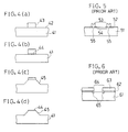
- the sixth example is different from Example 1 in that an inclined area is formed on the border between the transparent part and the opaque part in the step of etching of the opaque pattern.
- a shield film 42 was deposited on a substrate 41 made of quartz, on which a resist layer to electron beam was formed followed by drawing thereon a predetermined pattern by use of electron beam lithographic system before development to obtain a resist pattern 43 (see Fig. 4(a)).
- the shield film 42 was then etched by normal liquid phase etching using the resist pattern 43 as a mask to form an opaque pattern 44 (see Fig. 4(b)).
- the quartz substrate 41 was etched by reactive etching using the resist pattern 43 as a mask to form a pattern 45.
- the pattern must become larger as etching proceeds.
- Etching of silicon dioxide is conducted generally by using reaction gas mainly made of CF 4 + H 2 or CHF 3 .
- the gas is likely to form polymer in vapor phase.
- polymer is deposited on the side wall part to make thicker the resultant pattern and taper the etched part during etching.
- the known etching technique forms the inclined area 45 on the quartz substrate adjacent to the opaque region. (see Fig. 4(c)).
- the embodiments of the present invention each provide a mask for photolithography which comprises a transparent substrate to admit visible light or ultraviolet for transferring a mask pattern which is opaque to the light and formed on the substrate, wherein a step portion having an inclined area is provided on the transparent part adjacent to the opaque pattern, so that drawing of the pattern by electron beam lithography is required only once, thereby allowing formation of a self-aligned phase shifting region.
- the phase shifting part is made of a SOG film, a CVD deposition film or the transparent substrate itself, thereby having little fear of being damaged in washing process or the like.
- the inclined area formed on the border between the transparent part and the opaque part allows phase shifting of light passing through the phase shifting part to be continuously increased from the transparent part to the opaque part.
- phase shifting at the edge of the transparent part is set to a value approaching 180°, sharp shaping up can be confined to the edge part of light flux passing through the transparent part without unexpectedly decaying the applied light as a whole, leading to a remarkable improvement of the resolution of photolithography in comparison with the conventional phase shifting mask.
Landscapes
- Physics & Mathematics (AREA)
- General Physics & Mathematics (AREA)
- Preparing Plates And Mask In Photomechanical Process (AREA)
Claims (16)
- Fotolithographiemaske mit:einen Substrat (1; 21; 31; 41; 71; 81; 91), das für Licht mit einer vorbestimmten Wellenlänge transparent ist;einen undurchsichtigen Muster (4; 24; 34; 44; 74; 84; 94), das auf dem Substrat vorhanden ist, um Licht an Durchlaufen durch dasselbe zu hindern; undeiner Phasenschiebeeinrichtung (5; 26; 36; 45; 75; 85; 95), die für das Licht transparent ist und angrenzend an den Rand des undurchsichtigen Musters auf den Substrat vorhanden ist;
dadurch gekennzeichnet, dass die Phasenschiebeeinrichtung einen Stufenabschnitt (6; 26; 36; 45; 76; 86; 96) mit einer in Bezug auf das Substrat geneigten Fläche aufweist, wobei der dickste Teil des transparenten Stufenabschnitts am nächsten beim Rand des undurchsichtigen Musters liegt und eine Höhe aufweist, die in Wesentlichen - Maske nach Anspruch 1, bei der der auf dem Substrat (31) vorhandene transparente Film (36) den transparenten Stufenabschnitt (36) bildet, wobei der transparente Film nur im Bereich vorhanden ist, der an den Rand des undurchsichtigen Musters (34) angrenzt.
- Maske nach Anspruch 1, bei der der Rand des undurchsichtigen Musters (4; 24; 34; 74; 84; 94) als Seitenwand ausgebildet ist, die im Wesentlichen rechtwinklig zum Substrat (1; 21; 31; 71; 81; 91) steht, um eine im wesentlichen rechtwinklige Stufe auszubilden, und bei der der transparente Stufenabschnitt aus einem transparenten Film besteht, der zumindest auf der Seitenwand so ausgebildet ist, dass die schräge Fläche ungefähr als Quadrantenbogen ausgebildet ist.
- Maske nach Anspruch 1, bei der ein auf dem Substrat (1; 21; 71; 81; 91) vorhandener transparenter Film (5; 26; 75; 85; 95) den transparenten Stufenabschnitt bildet und sich über das undurchsichtige Muster (4; 24; 74; 84; 94) erstreckt.
- Maske nach Anspruch 1, bei der der Rand des undurchsichtigen Musters (4; 24; 74; 84; 94) als Seitenwand ausgebildet ist, die im Wesentlichen rechtwinklig zum Substrat (1; 21; 71; 81; 91) verläuft, um eine im Wesentlichen rechtwinklige Stufe zu bilden, und bei der sich ein auf dem Substrat vorhandener transparenter Film (5; 26; 75; 85; 95) über das undurchsichtige Muster erstreckt und den transparenten Stufenabschnitt (6; 26; 76; 86; 96) über dem Rand des undurchsichtigen Musters mit einer Form ungefähr eines Quadrantenbogens bildet.
- Maske nach Anspruch 1, bei der das Substrat (21; 41) am Rand des undurchsichtigen Musters (24; 44) oder angrenzend an diesen einen geätzten Abschnitt enthält, und bei der der transparente Stufenabschnitt auf dem geätzten Abschnitt des Substrats ausgebildet oder durch diesen gebildet ist.
- Maske nach Anspruch 6, bei der der geätzte Abschnitt des Substrats (21) eine im Wesentlichen vertikale Randfläche ist, die mit den oben liegenden Rand des undurchsichtigen Musters eine in Wesentlichen vertikale Stufe bildet, wobei der transparente Stufenabschnitt einen transparenten Film (26) aufweist, der so zumindest auf der im wesentlichen vertikalen Stufe so ausgebildet ist, dass die schräge Fläche ungefähr als Quadrantenbogen ausgebildet ist.
- Maske nach einem Ansprüche 3, 5 und 7, bei dem die in Wesentlichen vertikale Stufe eine Höhe aufweist, die im Wesentlichen
- Maske nach Anspruch 6, bei der der geätzte Abschnitt des Substrats (41) den transparenten Stufenabschnitt bildet und die schräge Fläche (45) enthält.
- Maske nach Anspruch 1, bei der Abschnitte einer beim Strukturieren des undurchsichtigen Musters (74; 84; 94) verwendeten Resistschicht (73; 83; 93) über dem undurchsichtigen Muster liegen.
- Verfahren zum Herstellen einer Fotolithographiemaske mit einen für Licht mit einer vorbestimmten Wellenlänge durchlässigen Substrat, wobei das Verfahren die folgenden Schritte aufweist:(1) Herstellen eines für das Licht undurchsichtigen Abschirmungsfilms auf den Substrat;(2) Herstellen eines Resistfilms für einen Elektronenstrahl auf dem Abschirmungsfilm sowie Herstellen eines Resistmusters auf dem Resistfilm durch Zeichnen eines vorbestimmten Musters mit einer Elektronenstrahl-Lithographievorrichtung, und anschließendes Entwickeln des so hergestellten Musters;(3) Ätzen des Abschirmungsfilms durch anisotropes Ätzen unter Verwendung des Resistmusters als Maske, um auf dem Substrat ein undurchsichtiges Musters auszubilden; und(4) Auflaminieren eines transparenten Films auf das Substrat einschließlich dem undurchsichtigen Muster durch Entfernen oder ohne Entfernen des Resistmusters, wobei eine Phasenschiebemaske mit einem transparenten Stufenabschnitt hergestellt wird, der angrenzend an den Rand des undurchsichtigen Musters ausgebildet ist und eine Oberfläche aufweist, die in Bezug auf das Substrat geneigt ist, und wobei der dickste Teil des transparenten Stufenabschnitts am Nächsten beim Rand des undurchsichtigen Musters liegt und eine Höhe aufweist, die im Wesentlichen
- Verfahren zum Herstellen einer Fotolithographiemaske nach Anspruch 11, bei dem der im Schritt (4) auflaminierte Film mit Ausnahme desjenigen Abschnitts entfernt wird, der das undurchsichtige Muster umgibt, wobei dieser umgebende Abschnitt den transparenten Stufenabschnitt bildet.
- Verfahren zum Herstellen einer Fotolithographiemaske nach Anspruch 11, bei der der Ätzschritt (3) das Ätzen des Substrats unter Verwendung des Resistmusters als Maske nach dem Ätzen des Abschirmungsfilms beinhaltet, wobei der geätzte Teil des Substrats und der oben liegende Rand des undurchsichtigen Musters eine Stufe bilden, auf die der transparente Film im Schritt (4) auflaminiert wird.
- Verfahren zum Herstellen einer Fotolithographiemaske nach Anspruch 11, bei der Abschnitte des Resistmusters auf den entsprechenden Abschnitten des undurchsichtigen Musters verbleiben, so dass dann, wenn der Schritt (4) ausgeführt wird, der transparente Film auf eine Stufe auflaminiert wird, die den Rand des undurchsichtigen Musters und den oben liegenden Rand des verbliebenen Resistmusters umfasst.
- Verfahren zum Herstellen einer Fotolithographiemaske nach Anspruch 11, bei der die Höhendifferenz (Td) zwischen den Niveaus der jeweiligen Oberflächen über den undurchsichtigen Muster (84; 94) einerseits und dem Substrat (81; 91) andererseits, auf denen der transparente Film (85; 95) vorhanden ist,
- Verfahren zum Herstellen einer Fotolithographiemaske nach Anspruch 11, bei der die Höhe einer Stufe am Rand des undurchsichtigen Musters, die diesen Rand enthält, angrenzend an den der transparente Stufenabschnitt im Schritt (4) hergestellt wird, im Wesentlichen
Applications Claiming Priority (6)
| Application Number | Priority Date | Filing Date | Title |
|---|---|---|---|
| JP10583290 | 1990-04-19 | ||
| JP105832/90 | 1990-04-19 | ||
| JP10583290 | 1990-04-19 | ||
| JP17192090 | 1990-06-28 | ||
| JP17192090A JP2566048B2 (ja) | 1990-04-19 | 1990-06-28 | 光露光用マスク及びその製造方法 |
| JP171920/90 | 1991-06-18 |
Publications (2)
| Publication Number | Publication Date |
|---|---|
| EP0453310A1 EP0453310A1 (de) | 1991-10-23 |
| EP0453310B1 true EP0453310B1 (de) | 2000-07-12 |
Family
ID=26446055
Family Applications (1)
| Application Number | Title | Priority Date | Filing Date |
|---|---|---|---|
| EP91303545A Expired - Lifetime EP0453310B1 (de) | 1990-04-19 | 1991-04-19 | Maske für Photolithographie |
Country Status (5)
| Country | Link |
|---|---|
| US (1) | US5389474A (de) |
| EP (1) | EP0453310B1 (de) |
| JP (1) | JP2566048B2 (de) |
| KR (1) | KR940007788B1 (de) |
| DE (1) | DE69132303T2 (de) |
Cited By (1)
| Publication number | Priority date | Publication date | Assignee | Title |
|---|---|---|---|---|
| CN106154743A (zh) * | 2015-03-24 | 2016-11-23 | 中芯国际集成电路制造(上海)有限公司 | 掩模及其形成方法 |
Families Citing this family (24)
| Publication number | Priority date | Publication date | Assignee | Title |
|---|---|---|---|---|
| EP0843217A3 (de) * | 1990-09-10 | 1998-12-16 | Fujitsu Limited | Optische Phasenmaske und Verfahren zur Herstellung |
| EP0524741A1 (de) * | 1991-07-12 | 1993-01-27 | Motorola, Inc. | Verfahren zur Erhöhung der Bildauflösung einer Maske für die Herstellung von Halbleiterschaltungen |
| US5281500A (en) * | 1991-09-04 | 1994-01-25 | Micron Technology, Inc. | Method of preventing null formation in phase shifted photomasks |
| JP2759582B2 (ja) * | 1991-09-05 | 1998-05-28 | 三菱電機株式会社 | フォトマスクおよびその製造方法 |
| US5382483A (en) * | 1992-01-13 | 1995-01-17 | International Business Machines Corporation | Self-aligned phase-shifting mask |
| EP0553543B1 (de) * | 1992-01-31 | 1997-12-29 | Mitsubishi Denki Kabushiki Kaisha | Phasenverschiebungsmaske und Verfahren zur Erzeugung eines Fotolackmusters unter Verwendung dieser Maske |
| KR100263900B1 (ko) * | 1993-03-04 | 2000-09-01 | 윤종용 | 마스크 및 그 제조방법 |
| US5642183A (en) * | 1993-08-27 | 1997-06-24 | Sharp Kabushiki Kaisha | Spatial filter used in a reduction-type projection printing apparatus |
| US5532089A (en) * | 1993-12-23 | 1996-07-02 | International Business Machines Corporation | Simplified fabrication methods for rim phase-shift masks |
| TW270219B (de) * | 1994-05-31 | 1996-02-11 | Advanced Micro Devices Inc | |
| US5566011A (en) * | 1994-12-08 | 1996-10-15 | Luncent Technologies Inc. | Antiflector black matrix having successively a chromium oxide layer, a molybdenum layer and a second chromium oxide layer |
| US5989752A (en) * | 1996-05-29 | 1999-11-23 | Chiu; Tzu-Yin | Reconfigurable mask |
| KR100230376B1 (ko) * | 1996-10-16 | 1999-11-15 | 윤종용 | 위상 시프트 마스크 및 그 제조방법 |
| JP3080023B2 (ja) * | 1997-02-20 | 2000-08-21 | 日本電気株式会社 | 露光用フォトマスク |
| TW497165B (en) * | 1999-06-30 | 2002-08-01 | Hitachi Ltd | Method for manufacturing semiconductor integrated circuit device, optical mask used therefor, method for manufacturing the same, and mask blanks used therefor |
| JP3760086B2 (ja) * | 2000-07-07 | 2006-03-29 | 株式会社ルネサステクノロジ | フォトマスクの製造方法 |
| TW541605B (en) * | 2000-07-07 | 2003-07-11 | Hitachi Ltd | Fabrication method of semiconductor integrated circuit device |
| JP2002184669A (ja) | 2000-12-14 | 2002-06-28 | Hitachi Ltd | 半導体集積回路装置の製造方法 |
| JP2002196470A (ja) | 2000-12-26 | 2002-07-12 | Hitachi Ltd | フォトマスクの製造方法および半導体集積回路装置の製造方法 |
| JP2002202585A (ja) | 2000-12-27 | 2002-07-19 | Hitachi Ltd | フォトマスクの製造方法および半導体集積回路装置の製造方法 |
| JP3827544B2 (ja) | 2001-08-31 | 2006-09-27 | 株式会社ルネサステクノロジ | 半導体集積回路装置の製造方法 |
| JP2003121977A (ja) * | 2001-10-12 | 2003-04-23 | Hitachi Ltd | 半導体集積回路装置の製造方法およびマスク |
| JP2003287875A (ja) * | 2002-01-24 | 2003-10-10 | Hitachi Ltd | マスクの製造方法および半導体集積回路装置の製造方法 |
| JP3754378B2 (ja) * | 2002-02-14 | 2006-03-08 | 株式会社ルネサステクノロジ | 半導体集積回路装置の製造方法 |
Family Cites Families (13)
| Publication number | Priority date | Publication date | Assignee | Title |
|---|---|---|---|---|
| US3986876A (en) * | 1974-05-24 | 1976-10-19 | The United States Of America As Represented By The Secretary Of The Navy | Method for making a mask having a sloped relief |
| JPS55163539A (en) * | 1979-06-06 | 1980-12-19 | Nec Kyushu Ltd | Photo mask |
| DE3015142A1 (de) * | 1980-04-19 | 1981-12-03 | Deutsche Itt Industries Gmbh, 7800 Freiburg | Photomaske, verfahren zur herstellung sowie deren verwendung zur erzeugung kleiner halbleiterstrukturen |
| JPS576849A (en) * | 1980-06-13 | 1982-01-13 | Matsushita Electric Ind Co Ltd | Photomask and its preparation |
| JPS5741639A (en) * | 1980-08-25 | 1982-03-08 | Fujitsu Ltd | Treatment of photomask to provide electric conductivity |
| JPS5760335A (en) * | 1980-09-29 | 1982-04-12 | Hitachi Ltd | Exposure mask |
| JPS59143156A (ja) * | 1983-02-07 | 1984-08-16 | Seiko Epson Corp | ガラス・マスク |
| JPS60128447A (ja) * | 1983-12-14 | 1985-07-09 | Fujitsu Ltd | フオトマスク |
| JP2710967B2 (ja) * | 1988-11-22 | 1998-02-10 | 株式会社日立製作所 | 集積回路装置の製造方法 |
| EP0653679B1 (de) * | 1989-04-28 | 2002-08-21 | Fujitsu Limited | Maske, Verfahren zur Herstellung der Maske und Verfahren zur Musterherstellung mit einer Maske |
| JPH03172848A (ja) * | 1989-12-01 | 1991-07-26 | Mitsubishi Electric Corp | ホトマスクの製造方法 |
| JPH03172847A (ja) * | 1989-12-01 | 1991-07-26 | Mitsubishi Electric Corp | ホトマスクの製造方法 |
| JPH03211554A (ja) * | 1990-01-17 | 1991-09-17 | Fujitsu Ltd | 位相シフトマスクの製造方法 |
-
1990
- 1990-06-28 JP JP17192090A patent/JP2566048B2/ja not_active Expired - Fee Related
-
1991
- 1991-04-19 KR KR1019910006311A patent/KR940007788B1/ko not_active Expired - Lifetime
- 1991-04-19 EP EP91303545A patent/EP0453310B1/de not_active Expired - Lifetime
- 1991-04-19 DE DE69132303T patent/DE69132303T2/de not_active Expired - Lifetime
-
1993
- 1993-04-12 US US08/047,056 patent/US5389474A/en not_active Expired - Lifetime
Cited By (1)
| Publication number | Priority date | Publication date | Assignee | Title |
|---|---|---|---|---|
| CN106154743A (zh) * | 2015-03-24 | 2016-11-23 | 中芯国际集成电路制造(上海)有限公司 | 掩模及其形成方法 |
Also Published As
| Publication number | Publication date |
|---|---|
| US5389474A (en) | 1995-02-14 |
| JP2566048B2 (ja) | 1996-12-25 |
| EP0453310A1 (de) | 1991-10-23 |
| JPH043412A (ja) | 1992-01-08 |
| DE69132303T2 (de) | 2000-12-21 |
| KR940007788B1 (ko) | 1994-08-25 |
| DE69132303D1 (de) | 2000-08-17 |
Similar Documents
| Publication | Publication Date | Title |
|---|---|---|
| EP0453310B1 (de) | Maske für Photolithographie | |
| US5750290A (en) | Photo mask and fabrication process therefor | |
| US6562522B1 (en) | Photomasking | |
| JP3262302B2 (ja) | 位相シフトフォトマスク、位相シフトフォトマスク用ブランクス及びそれらの製造方法 | |
| US7838183B2 (en) | Multi-layer, attenuated phase-shifting mask | |
| EP0585872B1 (de) | Verfahren zur Herstellung einer Phasenschiebermaske oder eines Phasenschiebermasken-Rohlings | |
| JP3368947B2 (ja) | レティクル及びレティクル・ブランク | |
| JPH07209851A (ja) | リソグラフィ露光マスクおよびその製造方法 | |
| US5902702A (en) | Phase shift mask, blank for phase shift mask, and method of manufacturing phase shift mask | |
| JPH08272071A (ja) | 位相シフトマスクとその製造方法、ならびにマスクブランク | |
| JPH0876353A (ja) | 位相シフトマスクの製造方法 | |
| US5849438A (en) | Phase shift mask and method for fabricating the same | |
| US7745842B2 (en) | Graytone mask and method thereof | |
| JP3312702B2 (ja) | 位相シフトフォトマスク及び位相シフトフォトマスク用ブランクス | |
| JPH0566554A (ja) | フオトマスク | |
| JP2002268201A (ja) | 位相シフトフォトマスク及び位相シフトフォトマスク用ブランクスの製造方法 | |
| JPH05142745A (ja) | 位相シフトマスク及びマスクの製造方法 | |
| JPH04368947A (ja) | 位相シフトマスクの作成方法 | |
| JP3241068B2 (ja) | 光露光用マスク及びその形成方法 | |
| JP3173314B2 (ja) | 位相シフトマスクの製造方法 | |
| JPH06347993A (ja) | 位相シフトマスクおよびその製造方法 | |
| JP3046631B2 (ja) | 位相シフトフォトマスクの製造方法 | |
| JPH07159971A (ja) | 光学マスクブランクと光学マスクおよびそれらの製造方法 | |
| JPH05281702A (ja) | 位相シフトマスクの製造方法 | |
| EP0590627A2 (de) | Photomaske zur Herstellung von Halbeitern |
Legal Events
| Date | Code | Title | Description |
|---|---|---|---|
| PUAI | Public reference made under article 153(3) epc to a published international application that has entered the european phase |
Free format text: ORIGINAL CODE: 0009012 |
|
| 17P | Request for examination filed |
Effective date: 19910510 |
|
| AK | Designated contracting states |
Kind code of ref document: A1 Designated state(s): DE FR GB |
|
| 17Q | First examination report despatched |
Effective date: 19940701 |
|
| GRAG | Despatch of communication of intention to grant |
Free format text: ORIGINAL CODE: EPIDOS AGRA |
|
| GRAG | Despatch of communication of intention to grant |
Free format text: ORIGINAL CODE: EPIDOS AGRA |
|
| GRAH | Despatch of communication of intention to grant a patent |
Free format text: ORIGINAL CODE: EPIDOS IGRA |
|
| GRAH | Despatch of communication of intention to grant a patent |
Free format text: ORIGINAL CODE: EPIDOS IGRA |
|
| GRAA | (expected) grant |
Free format text: ORIGINAL CODE: 0009210 |
|
| AK | Designated contracting states |
Kind code of ref document: B1 Designated state(s): DE FR GB |
|
| REF | Corresponds to: |
Ref document number: 69132303 Country of ref document: DE Date of ref document: 20000817 |
|
| ET | Fr: translation filed | ||
| PLBE | No opposition filed within time limit |
Free format text: ORIGINAL CODE: 0009261 |
|
| STAA | Information on the status of an ep patent application or granted ep patent |
Free format text: STATUS: NO OPPOSITION FILED WITHIN TIME LIMIT |
|
| 26N | No opposition filed | ||
| REG | Reference to a national code |
Ref country code: GB Ref legal event code: IF02 |
|
| PGFP | Annual fee paid to national office [announced via postgrant information from national office to epo] |
Ref country code: GB Payment date: 20100325 Year of fee payment: 20 |
|
| PGFP | Annual fee paid to national office [announced via postgrant information from national office to epo] |
Ref country code: FR Payment date: 20100521 Year of fee payment: 20 |
|
| PGFP | Annual fee paid to national office [announced via postgrant information from national office to epo] |
Ref country code: DE Payment date: 20100430 Year of fee payment: 20 |
|
| REG | Reference to a national code |
Ref country code: DE Ref legal event code: R071 Ref document number: 69132303 Country of ref document: DE |
|
| REG | Reference to a national code |
Ref country code: GB Ref legal event code: PE20 Expiry date: 20110418 |
|
| PG25 | Lapsed in a contracting state [announced via postgrant information from national office to epo] |
Ref country code: GB Free format text: LAPSE BECAUSE OF EXPIRATION OF PROTECTION Effective date: 20110418 |
|
| PG25 | Lapsed in a contracting state [announced via postgrant information from national office to epo] |
Ref country code: DE Free format text: LAPSE BECAUSE OF EXPIRATION OF PROTECTION Effective date: 20110419 |