EP0525779A2 - Verfahren zur Herstellung eines optischen Halbleiterelements - Google Patents
Verfahren zur Herstellung eines optischen Halbleiterelements Download PDFInfo
- Publication number
- EP0525779A2 EP0525779A2 EP92113029A EP92113029A EP0525779A2 EP 0525779 A2 EP0525779 A2 EP 0525779A2 EP 92113029 A EP92113029 A EP 92113029A EP 92113029 A EP92113029 A EP 92113029A EP 0525779 A2 EP0525779 A2 EP 0525779A2
- Authority
- EP
- European Patent Office
- Prior art keywords
- active layer
- amplifier
- semiconductor
- ridge
- gain
- Prior art date
- Legal status (The legal status is an assumption and is not a legal conclusion. Google has not performed a legal analysis and makes no representation as to the accuracy of the status listed.)
- Granted
Links
Images

Classifications
-
- H—ELECTRICITY
- H10—SEMICONDUCTOR DEVICES; ELECTRIC SOLID-STATE DEVICES NOT OTHERWISE PROVIDED FOR
- H10H—INORGANIC LIGHT-EMITTING SEMICONDUCTOR DEVICES HAVING POTENTIAL BARRIERS
- H10H20/00—Individual inorganic light-emitting semiconductor devices having potential barriers, e.g. light-emitting diodes [LED]
- H10H20/80—Constructional details
- H10H20/84—Coatings, e.g. passivation layers or antireflective coatings
-
- H—ELECTRICITY
- H01—ELECTRIC ELEMENTS
- H01S—DEVICES USING THE PROCESS OF LIGHT AMPLIFICATION BY STIMULATED EMISSION OF RADIATION [LASER] TO AMPLIFY OR GENERATE LIGHT; DEVICES USING STIMULATED EMISSION OF ELECTROMAGNETIC RADIATION IN WAVE RANGES OTHER THAN OPTICAL
- H01S5/00—Semiconductor lasers
- H01S5/20—Structure or shape of the semiconductor body to guide the optical wave ; Confining structures perpendicular to the optical axis, e.g. index or gain guiding, stripe geometry, broad area lasers, gain tailoring, transverse or lateral reflectors, special cladding structures, MQW barrier reflection layers
- H01S5/22—Structure or shape of the semiconductor body to guide the optical wave ; Confining structures perpendicular to the optical axis, e.g. index or gain guiding, stripe geometry, broad area lasers, gain tailoring, transverse or lateral reflectors, special cladding structures, MQW barrier reflection layers having a ridge or stripe structure
- H01S5/227—Buried mesa structure ; Striped active layer
-
- H—ELECTRICITY
- H10—SEMICONDUCTOR DEVICES; ELECTRIC SOLID-STATE DEVICES NOT OTHERWISE PROVIDED FOR
- H10H—INORGANIC LIGHT-EMITTING SEMICONDUCTOR DEVICES HAVING POTENTIAL BARRIERS
- H10H20/00—Individual inorganic light-emitting semiconductor devices having potential barriers, e.g. light-emitting diodes [LED]
- H10H20/01—Manufacture or treatment
- H10H20/011—Manufacture or treatment of bodies, e.g. forming semiconductor layers
- H10H20/013—Manufacture or treatment of bodies, e.g. forming semiconductor layers having light-emitting regions comprising only Group III-V materials
-
- H—ELECTRICITY
- H10—SEMICONDUCTOR DEVICES; ELECTRIC SOLID-STATE DEVICES NOT OTHERWISE PROVIDED FOR
- H10P—GENERIC PROCESSES OR APPARATUS FOR THE MANUFACTURE OR TREATMENT OF DEVICES COVERED BY CLASS H10
- H10P14/00—Formation of materials, e.g. in the shape of layers or pillars
- H10P14/20—Formation of materials, e.g. in the shape of layers or pillars of semiconductor materials
- H10P14/24—Formation of materials, e.g. in the shape of layers or pillars of semiconductor materials using chemical vapour deposition [CVD]
-
- H—ELECTRICITY
- H10—SEMICONDUCTOR DEVICES; ELECTRIC SOLID-STATE DEVICES NOT OTHERWISE PROVIDED FOR
- H10P—GENERIC PROCESSES OR APPARATUS FOR THE MANUFACTURE OR TREATMENT OF DEVICES COVERED BY CLASS H10
- H10P14/00—Formation of materials, e.g. in the shape of layers or pillars
- H10P14/20—Formation of materials, e.g. in the shape of layers or pillars of semiconductor materials
- H10P14/27—Formation of materials, e.g. in the shape of layers or pillars of semiconductor materials using selective deposition, e.g. simultaneous growth of monocrystalline and non-monocrystalline semiconductor materials
- H10P14/271—Formation of materials, e.g. in the shape of layers or pillars of semiconductor materials using selective deposition, e.g. simultaneous growth of monocrystalline and non-monocrystalline semiconductor materials characterised by the preparation of substrate for selective deposition
-
- H—ELECTRICITY
- H10—SEMICONDUCTOR DEVICES; ELECTRIC SOLID-STATE DEVICES NOT OTHERWISE PROVIDED FOR
- H10P—GENERIC PROCESSES OR APPARATUS FOR THE MANUFACTURE OR TREATMENT OF DEVICES COVERED BY CLASS H10
- H10P14/00—Formation of materials, e.g. in the shape of layers or pillars
- H10P14/20—Formation of materials, e.g. in the shape of layers or pillars of semiconductor materials
- H10P14/29—Formation of materials, e.g. in the shape of layers or pillars of semiconductor materials characterised by the substrates
- H10P14/2901—Materials
- H10P14/2907—Materials being Group IIIA-VA materials
- H10P14/2909—Phosphides
-
- H—ELECTRICITY
- H10—SEMICONDUCTOR DEVICES; ELECTRIC SOLID-STATE DEVICES NOT OTHERWISE PROVIDED FOR
- H10P—GENERIC PROCESSES OR APPARATUS FOR THE MANUFACTURE OR TREATMENT OF DEVICES COVERED BY CLASS H10
- H10P14/00—Formation of materials, e.g. in the shape of layers or pillars
- H10P14/20—Formation of materials, e.g. in the shape of layers or pillars of semiconductor materials
- H10P14/34—Deposited materials, e.g. layers
- H10P14/3402—Deposited materials, e.g. layers characterised by the chemical composition
- H10P14/3414—Deposited materials, e.g. layers characterised by the chemical composition being group IIIA-VIA materials
- H10P14/3418—Phosphides
-
- H—ELECTRICITY
- H10—SEMICONDUCTOR DEVICES; ELECTRIC SOLID-STATE DEVICES NOT OTHERWISE PROVIDED FOR
- H10P—GENERIC PROCESSES OR APPARATUS FOR THE MANUFACTURE OR TREATMENT OF DEVICES COVERED BY CLASS H10
- H10P14/00—Formation of materials, e.g. in the shape of layers or pillars
- H10P14/20—Formation of materials, e.g. in the shape of layers or pillars of semiconductor materials
- H10P14/34—Deposited materials, e.g. layers
- H10P14/3402—Deposited materials, e.g. layers characterised by the chemical composition
- H10P14/3414—Deposited materials, e.g. layers characterised by the chemical composition being group IIIA-VIA materials
- H10P14/3421—Arsenides
-
- H—ELECTRICITY
- H01—ELECTRIC ELEMENTS
- H01S—DEVICES USING THE PROCESS OF LIGHT AMPLIFICATION BY STIMULATED EMISSION OF RADIATION [LASER] TO AMPLIFY OR GENERATE LIGHT; DEVICES USING STIMULATED EMISSION OF ELECTROMAGNETIC RADIATION IN WAVE RANGES OTHER THAN OPTICAL
- H01S5/00—Semiconductor lasers
- H01S5/20—Structure or shape of the semiconductor body to guide the optical wave ; Confining structures perpendicular to the optical axis, e.g. index or gain guiding, stripe geometry, broad area lasers, gain tailoring, transverse or lateral reflectors, special cladding structures, MQW barrier reflection layers
- H01S5/22—Structure or shape of the semiconductor body to guide the optical wave ; Confining structures perpendicular to the optical axis, e.g. index or gain guiding, stripe geometry, broad area lasers, gain tailoring, transverse or lateral reflectors, special cladding structures, MQW barrier reflection layers having a ridge or stripe structure
- H01S5/227—Buried mesa structure ; Striped active layer
- H01S5/2272—Buried mesa structure ; Striped active layer grown by a mask induced selective growth
-
- H—ELECTRICITY
- H01—ELECTRIC ELEMENTS
- H01S—DEVICES USING THE PROCESS OF LIGHT AMPLIFICATION BY STIMULATED EMISSION OF RADIATION [LASER] TO AMPLIFY OR GENERATE LIGHT; DEVICES USING STIMULATED EMISSION OF ELECTROMAGNETIC RADIATION IN WAVE RANGES OTHER THAN OPTICAL
- H01S5/00—Semiconductor lasers
- H01S5/50—Amplifier structures not provided for in groups H01S5/02 - H01S5/30
- H01S5/5036—Amplifier structures not provided for in groups H01S5/02 - H01S5/30 the arrangement being polarisation-selective
-
- Y—GENERAL TAGGING OF NEW TECHNOLOGICAL DEVELOPMENTS; GENERAL TAGGING OF CROSS-SECTIONAL TECHNOLOGIES SPANNING OVER SEVERAL SECTIONS OF THE IPC; TECHNICAL SUBJECTS COVERED BY FORMER USPC CROSS-REFERENCE ART COLLECTIONS [XRACs] AND DIGESTS
- Y10—TECHNICAL SUBJECTS COVERED BY FORMER USPC
- Y10S—TECHNICAL SUBJECTS COVERED BY FORMER USPC CROSS-REFERENCE ART COLLECTIONS [XRACs] AND DIGESTS
- Y10S148/00—Metal treatment
- Y10S148/026—Deposition thru hole in mask
Definitions
- the ripple of the gain must be considered.
- the ripple is caused by reflection of signal light propagating through a waveguide in the amplifier on the facet of an LD amplifier element.
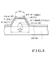
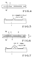
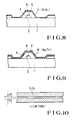
- a method of manufacturing an optical semiconductor element including at least the steps of forming a mask having a stripe-like gap or interval on a semiconductor substrate, epitaxially growing a semiconductor ridge including an active layer on only an exposed gap portion of the semiconductor substrate, and epitaxially growing a semiconductor cladding layer to cover the ridge, wherein a width of the active layer is less than 5,000 ⁇ .
- This embodiment is not limited to the compositions of the illustrated active layer, cladding layer, capping layer, and window structure portion.
- an electrode having another composition may be used.
Landscapes
- Physics & Mathematics (AREA)
- Geometry (AREA)
- Condensed Matter Physics & Semiconductors (AREA)
- General Physics & Mathematics (AREA)
- Electromagnetism (AREA)
- Optics & Photonics (AREA)
- Semiconductor Lasers (AREA)
- Recrystallisation Techniques (AREA)
Applications Claiming Priority (2)
| Application Number | Priority Date | Filing Date | Title |
|---|---|---|---|
| JP216027/91 | 1991-07-31 | ||
| JP3216027A JP2876839B2 (ja) | 1991-07-31 | 1991-07-31 | 光半導体素子の製造方法 |
Publications (3)
| Publication Number | Publication Date |
|---|---|
| EP0525779A2 true EP0525779A2 (de) | 1993-02-03 |
| EP0525779A3 EP0525779A3 (en) | 1993-04-07 |
| EP0525779B1 EP0525779B1 (de) | 1998-02-04 |
Family
ID=16682152
Family Applications (1)
| Application Number | Title | Priority Date | Filing Date |
|---|---|---|---|
| EP92113029A Expired - Lifetime EP0525779B1 (de) | 1991-07-31 | 1992-07-30 | Verfahren zur Herstellung eines optischen Halbleiterelements |
Country Status (4)
| Country | Link |
|---|---|
| US (1) | US5374587A (de) |
| EP (1) | EP0525779B1 (de) |
| JP (1) | JP2876839B2 (de) |
| DE (1) | DE69224335T2 (de) |
Cited By (5)
| Publication number | Priority date | Publication date | Assignee | Title |
|---|---|---|---|---|
| EP0637111A1 (de) * | 1993-07-29 | 1995-02-01 | Nec Corporation | Halbleitende optische Vorrichtung mit Mesa-Struktur, die seitlich von einer isolierenden Maske umgeben ist |
| EP0661783A1 (de) * | 1993-12-28 | 1995-07-05 | Nec Corporation | Verfahren zur Herstellung eines integrierten, optischen Halbleiterschaltkreises |
| FR2745961A1 (fr) * | 1996-03-05 | 1997-09-12 | Alcatel Optronics | Amplificateur optique a semi-conducteur |
| DE19911717A1 (de) * | 1999-03-16 | 2000-09-28 | Osram Opto Semiconductors Gmbh | Monolithisches elektrolumineszierendes Bauelement und Verfahren zu dessen Herstellung |
| EP2385478A1 (de) | 2004-12-28 | 2011-11-09 | Canon Kabushiki Kaisha | Bildverarbeitungsvorrichtung und Steuerverfahren |
Families Citing this family (3)
| Publication number | Priority date | Publication date | Assignee | Title |
|---|---|---|---|---|
| JP2004048079A (ja) * | 2000-05-17 | 2004-02-12 | Sony Corp | 半導体レーザ |
| JP2004048080A (ja) * | 2000-05-17 | 2004-02-12 | Sony Corp | 半導体レーザの製造方法 |
| US6731424B1 (en) * | 2001-03-15 | 2004-05-04 | Onetta, Inc. | Dynamic gain flattening in an optical communication system |
Family Cites Families (14)
| Publication number | Priority date | Publication date | Assignee | Title |
|---|---|---|---|---|
| US4077817A (en) * | 1975-12-31 | 1978-03-07 | Texas Instruments Incorporated | Making a semiconductor laser structure by liquid phase epitaxy |
| JPS568890A (en) * | 1979-06-27 | 1981-01-29 | Nec Corp | Semiconductor laser and manufacture thereof |
| JPS62144385A (ja) * | 1985-12-19 | 1987-06-27 | Fujitsu Ltd | 半導体レ−ザ及びその製造方法 |
| US4946802A (en) * | 1986-05-31 | 1990-08-07 | Mitsubishi Denki Kabushiki Kaisha | Semiconductor laser device fabricating method |
| GB8618373D0 (en) * | 1986-07-28 | 1986-09-03 | British Telecomm | Fabrication technique |
| JPH01220492A (ja) * | 1988-02-26 | 1989-09-04 | Mitsubishi Electric Corp | 半導体レーザ装置及びその製造方法 |
| KR900009229B1 (ko) * | 1988-04-28 | 1990-12-24 | 한국 과학기술원 | 선택적 에피택시법에 의한 표면 방출형 AlGaAs/GaAs 반도체 레이저 다이오드의 제조방법 |
| GB2222307B (en) * | 1988-07-22 | 1992-04-01 | Mitsubishi Electric Corp | Semiconductor laser |
| WO1990003055A1 (fr) * | 1988-09-01 | 1990-03-22 | Seiko Epson Corporation | Dispositif photo-emetteur et procede de production |
| JPH0314280A (ja) * | 1989-06-13 | 1991-01-22 | Nec Corp | 大出力半導体レーザ及びその製造方法 |
| JPH03126283A (ja) * | 1989-10-11 | 1991-05-29 | Toshiba Corp | 窓構造半導体レーザ素子の製造方法 |
| US5070510A (en) * | 1989-12-12 | 1991-12-03 | Sharp Kabushiki Kaisha | Semiconductor laser device |
| EP0643461B1 (de) * | 1990-08-24 | 1997-10-29 | Nec Corporation | Verfahren zur Herstellung einer optischen Halbleitervorrichtung |
| JPH04349622A (ja) * | 1991-05-28 | 1992-12-04 | Eastman Kodak Japan Kk | 量子デバイス製造方法 |
-
1991
- 1991-07-31 JP JP3216027A patent/JP2876839B2/ja not_active Expired - Fee Related
-
1992
- 1992-07-28 US US07/920,880 patent/US5374587A/en not_active Expired - Fee Related
- 1992-07-30 EP EP92113029A patent/EP0525779B1/de not_active Expired - Lifetime
- 1992-07-30 DE DE69224335T patent/DE69224335T2/de not_active Expired - Fee Related
Cited By (8)
| Publication number | Priority date | Publication date | Assignee | Title |
|---|---|---|---|---|
| EP0637111A1 (de) * | 1993-07-29 | 1995-02-01 | Nec Corporation | Halbleitende optische Vorrichtung mit Mesa-Struktur, die seitlich von einer isolierenden Maske umgeben ist |
| US5659565A (en) * | 1993-07-29 | 1997-08-19 | Kitamura; Shotaro | Semiconductor optical device with mesa structure which is surrounded laterally by insulating mask for preventing current from leaking directly from cladding layer to substrate and process of fabrication thereof |
| EP0661783A1 (de) * | 1993-12-28 | 1995-07-05 | Nec Corporation | Verfahren zur Herstellung eines integrierten, optischen Halbleiterschaltkreises |
| US6224667B1 (en) | 1993-12-28 | 2001-05-01 | Nec Corporation | Method for fabricating semiconductor light integrated circuit |
| FR2745961A1 (fr) * | 1996-03-05 | 1997-09-12 | Alcatel Optronics | Amplificateur optique a semi-conducteur |
| WO1997033353A1 (fr) * | 1996-03-05 | 1997-09-12 | Alcatel Optronics | Amplificateur optique a semi-conducteur |
| DE19911717A1 (de) * | 1999-03-16 | 2000-09-28 | Osram Opto Semiconductors Gmbh | Monolithisches elektrolumineszierendes Bauelement und Verfahren zu dessen Herstellung |
| EP2385478A1 (de) | 2004-12-28 | 2011-11-09 | Canon Kabushiki Kaisha | Bildverarbeitungsvorrichtung und Steuerverfahren |
Also Published As
| Publication number | Publication date |
|---|---|
| JPH0537092A (ja) | 1993-02-12 |
| JP2876839B2 (ja) | 1999-03-31 |
| EP0525779A3 (en) | 1993-04-07 |
| EP0525779B1 (de) | 1998-02-04 |
| DE69224335T2 (de) | 1998-09-17 |
| DE69224335D1 (de) | 1998-03-12 |
| US5374587A (en) | 1994-12-20 |
Similar Documents
| Publication | Publication Date | Title |
|---|---|---|
| JP3285426B2 (ja) | 半導体光集積素子及びその製造方法 | |
| EP0702435A1 (de) | Herstellungsverfahren für einen digital reflektiv einstellbarer Laser | |
| JP2842292B2 (ja) | 半導体光集積装置および製造方法 | |
| EP0526128B1 (de) | Verfahren zur Herstellung eines Halbleiterlasers mit verteilter Rückkoppelung | |
| EP0378098B1 (de) | Optische Halbleitervorrichtung | |
| US5737351A (en) | Semiconductor laser including ridge structure extending between window regions | |
| JP2937751B2 (ja) | 光半導体装置の製造方法 | |
| JPH0864906A (ja) | 半導体装置の製法 | |
| GB2287124A (en) | Semiconductor laser and method of fabrication | |
| EP0525779B1 (de) | Verfahren zur Herstellung eines optischen Halbleiterelements | |
| US6204078B1 (en) | Method of fabricating photonic semiconductor device using selective MOVPE | |
| JP3474917B2 (ja) | 半導体装置の製造方法 | |
| KR0174303B1 (ko) | 반도체장치 및 그 제조방법 | |
| EP1719003B1 (de) | Durch einschritt-mocvd hergestelltes vergrabene-heterostruktur-bauelement | |
| EP4122062B1 (de) | Elektroabsorptionsmodulierter laser | |
| EP0581604A2 (de) | Halbleiterlaservorrichtung | |
| US5805628A (en) | Semiconductor laser | |
| US6026106A (en) | Composite optical device | |
| JP2000188441A (ja) | 光半導体装置及びその製造方法 | |
| JPH08292336A (ja) | 光半導体集積回路の製造方法 | |
| JP3146821B2 (ja) | 半導体光集積素子の製造方法 | |
| WO2021209114A1 (en) | Optical device | |
| US20050008055A1 (en) | Facet passivation for edge emitting semiconductor lasers | |
| JP3022351B2 (ja) | 光半導体装置及びその製造方法 | |
| JPH08184721A (ja) | 光アイソレータ |
Legal Events
| Date | Code | Title | Description |
|---|---|---|---|
| PUAI | Public reference made under article 153(3) epc to a published international application that has entered the european phase |
Free format text: ORIGINAL CODE: 0009012 |
|
| AK | Designated contracting states |
Kind code of ref document: A2 Designated state(s): DE FR GB NL |
|
| PUAL | Search report despatched |
Free format text: ORIGINAL CODE: 0009013 |
|
| AK | Designated contracting states |
Kind code of ref document: A3 Designated state(s): DE FR GB NL |
|
| 17P | Request for examination filed |
Effective date: 19930301 |
|
| 17Q | First examination report despatched |
Effective date: 19940819 |
|
| GRAG | Despatch of communication of intention to grant |
Free format text: ORIGINAL CODE: EPIDOS AGRA |
|
| GRAG | Despatch of communication of intention to grant |
Free format text: ORIGINAL CODE: EPIDOS AGRA |
|
| GRAH | Despatch of communication of intention to grant a patent |
Free format text: ORIGINAL CODE: EPIDOS IGRA |
|
| GRAH | Despatch of communication of intention to grant a patent |
Free format text: ORIGINAL CODE: EPIDOS IGRA |
|
| GRAA | (expected) grant |
Free format text: ORIGINAL CODE: 0009210 |
|
| AK | Designated contracting states |
Kind code of ref document: B1 Designated state(s): DE FR GB NL |
|
| REF | Corresponds to: |
Ref document number: 69224335 Country of ref document: DE Date of ref document: 19980312 |
|
| ET | Fr: translation filed | ||
| PLBE | No opposition filed within time limit |
Free format text: ORIGINAL CODE: 0009261 |
|
| STAA | Information on the status of an ep patent application or granted ep patent |
Free format text: STATUS: NO OPPOSITION FILED WITHIN TIME LIMIT |
|
| 26N | No opposition filed | ||
| REG | Reference to a national code |
Ref country code: GB Ref legal event code: IF02 |
|
| PGFP | Annual fee paid to national office [announced via postgrant information from national office to epo] |
Ref country code: FR Payment date: 20030711 Year of fee payment: 12 |
|
| PGFP | Annual fee paid to national office [announced via postgrant information from national office to epo] |
Ref country code: NL Payment date: 20030730 Year of fee payment: 12 Ref country code: GB Payment date: 20030730 Year of fee payment: 12 |
|
| PGFP | Annual fee paid to national office [announced via postgrant information from national office to epo] |
Ref country code: DE Payment date: 20030807 Year of fee payment: 12 |
|
| PG25 | Lapsed in a contracting state [announced via postgrant information from national office to epo] |
Ref country code: GB Free format text: LAPSE BECAUSE OF NON-PAYMENT OF DUE FEES Effective date: 20040730 |
|
| PG25 | Lapsed in a contracting state [announced via postgrant information from national office to epo] |
Ref country code: NL Free format text: LAPSE BECAUSE OF NON-PAYMENT OF DUE FEES Effective date: 20050201 Ref country code: DE Free format text: LAPSE BECAUSE OF NON-PAYMENT OF DUE FEES Effective date: 20050201 |
|
| GBPC | Gb: european patent ceased through non-payment of renewal fee |
Effective date: 20040730 |
|
| PG25 | Lapsed in a contracting state [announced via postgrant information from national office to epo] |
Ref country code: FR Free format text: LAPSE BECAUSE OF NON-PAYMENT OF DUE FEES Effective date: 20050331 |
|
| NLV4 | Nl: lapsed or anulled due to non-payment of the annual fee |
Effective date: 20050201 |
|
| REG | Reference to a national code |
Ref country code: FR Ref legal event code: ST |