EP0525852A1 - Dispositif de reproduction - Google Patents
Dispositif de reproduction Download PDFInfo
- Publication number
- EP0525852A1 EP0525852A1 EP92201992A EP92201992A EP0525852A1 EP 0525852 A1 EP0525852 A1 EP 0525852A1 EP 92201992 A EP92201992 A EP 92201992A EP 92201992 A EP92201992 A EP 92201992A EP 0525852 A1 EP0525852 A1 EP 0525852A1
- Authority
- EP
- European Patent Office
- Prior art keywords
- rows
- pixels
- selection
- display device
- row
- Prior art date
- Legal status (The legal status is an assumption and is not a legal conclusion. Google has not performed a legal analysis and makes no representation as to the accuracy of the status listed.)
- Granted
Links
- 230000000694 effects Effects 0.000 abstract description 9
- 239000011159 matrix material Substances 0.000 abstract 1
- 230000005540 biological transmission Effects 0.000 description 6
- 230000008878 coupling Effects 0.000 description 5
- 238000010168 coupling process Methods 0.000 description 5
- 238000005859 coupling reaction Methods 0.000 description 5
- 239000004973 liquid crystal related substance Substances 0.000 description 5
- 230000006978 adaptation Effects 0.000 description 2
- AMGQUBHHOARCQH-UHFFFAOYSA-N indium;oxotin Chemical compound [In].[Sn]=O AMGQUBHHOARCQH-UHFFFAOYSA-N 0.000 description 2
- 239000002184 metal Substances 0.000 description 2
- 239000004988 Nematic liquid crystal Substances 0.000 description 1
- 230000002596 correlated effect Effects 0.000 description 1
- 230000000875 corresponding effect Effects 0.000 description 1
- 239000002178 crystalline material Substances 0.000 description 1
- 230000003247 decreasing effect Effects 0.000 description 1
- 230000001419 dependent effect Effects 0.000 description 1
- 230000001627 detrimental effect Effects 0.000 description 1
- 238000010586 diagram Methods 0.000 description 1
- 230000002349 favourable effect Effects 0.000 description 1
- 239000011521 glass Substances 0.000 description 1
- 238000007689 inspection Methods 0.000 description 1
- 239000007788 liquid Substances 0.000 description 1
- 239000000463 material Substances 0.000 description 1
- 238000000034 method Methods 0.000 description 1
- 239000000758 substrate Substances 0.000 description 1
- 239000000725 suspension Substances 0.000 description 1
- 230000001360 synchronised effect Effects 0.000 description 1
- 239000010409 thin film Substances 0.000 description 1
- 230000007704 transition Effects 0.000 description 1
- 239000012780 transparent material Substances 0.000 description 1
Images

Classifications
-
- G—PHYSICS
- G09—EDUCATION; CRYPTOGRAPHY; DISPLAY; ADVERTISING; SEALS
- G09G—ARRANGEMENTS OR CIRCUITS FOR CONTROL OF INDICATING DEVICES USING STATIC MEANS TO PRESENT VARIABLE INFORMATION
- G09G3/00—Control arrangements or circuits, of interest only in connection with visual indicators other than cathode-ray tubes
- G09G3/20—Control arrangements or circuits, of interest only in connection with visual indicators other than cathode-ray tubes for presentation of an assembly of a number of characters, e.g. a page, by composing the assembly by combination of individual elements arranged in a matrix no fixed position being assigned to or needed to be assigned to the individual characters or partial characters
- G09G3/34—Control arrangements or circuits, of interest only in connection with visual indicators other than cathode-ray tubes for presentation of an assembly of a number of characters, e.g. a page, by composing the assembly by combination of individual elements arranged in a matrix no fixed position being assigned to or needed to be assigned to the individual characters or partial characters by control of light from an independent source
- G09G3/36—Control arrangements or circuits, of interest only in connection with visual indicators other than cathode-ray tubes for presentation of an assembly of a number of characters, e.g. a page, by composing the assembly by combination of individual elements arranged in a matrix no fixed position being assigned to or needed to be assigned to the individual characters or partial characters by control of light from an independent source using liquid crystals
- G09G3/3611—Control of matrices with row and column drivers
- G09G3/367—Control of matrices with row and column drivers with a nonlinear element in series with the liquid crystal cell, e.g. a diode, or M.I.M. element
-
- G—PHYSICS
- G09—EDUCATION; CRYPTOGRAPHY; DISPLAY; ADVERTISING; SEALS
- G09G—ARRANGEMENTS OR CIRCUITS FOR CONTROL OF INDICATING DEVICES USING STATIC MEANS TO PRESENT VARIABLE INFORMATION
- G09G3/00—Control arrangements or circuits, of interest only in connection with visual indicators other than cathode-ray tubes
- G09G3/20—Control arrangements or circuits, of interest only in connection with visual indicators other than cathode-ray tubes for presentation of an assembly of a number of characters, e.g. a page, by composing the assembly by combination of individual elements arranged in a matrix no fixed position being assigned to or needed to be assigned to the individual characters or partial characters
- G09G3/34—Control arrangements or circuits, of interest only in connection with visual indicators other than cathode-ray tubes for presentation of an assembly of a number of characters, e.g. a page, by composing the assembly by combination of individual elements arranged in a matrix no fixed position being assigned to or needed to be assigned to the individual characters or partial characters by control of light from an independent source
- G09G3/36—Control arrangements or circuits, of interest only in connection with visual indicators other than cathode-ray tubes for presentation of an assembly of a number of characters, e.g. a page, by composing the assembly by combination of individual elements arranged in a matrix no fixed position being assigned to or needed to be assigned to the individual characters or partial characters by control of light from an independent source using liquid crystals
- G09G3/3607—Control arrangements or circuits, of interest only in connection with visual indicators other than cathode-ray tubes for presentation of an assembly of a number of characters, e.g. a page, by composing the assembly by combination of individual elements arranged in a matrix no fixed position being assigned to or needed to be assigned to the individual characters or partial characters by control of light from an independent source using liquid crystals for displaying colours or for displaying grey scales with a specific pixel layout, e.g. using sub-pixels
-
- G—PHYSICS
- G09—EDUCATION; CRYPTOGRAPHY; DISPLAY; ADVERTISING; SEALS
- G09G—ARRANGEMENTS OR CIRCUITS FOR CONTROL OF INDICATING DEVICES USING STATIC MEANS TO PRESENT VARIABLE INFORMATION
- G09G3/00—Control arrangements or circuits, of interest only in connection with visual indicators other than cathode-ray tubes
- G09G3/20—Control arrangements or circuits, of interest only in connection with visual indicators other than cathode-ray tubes for presentation of an assembly of a number of characters, e.g. a page, by composing the assembly by combination of individual elements arranged in a matrix no fixed position being assigned to or needed to be assigned to the individual characters or partial characters
- G09G3/34—Control arrangements or circuits, of interest only in connection with visual indicators other than cathode-ray tubes for presentation of an assembly of a number of characters, e.g. a page, by composing the assembly by combination of individual elements arranged in a matrix no fixed position being assigned to or needed to be assigned to the individual characters or partial characters by control of light from an independent source
- G09G3/36—Control arrangements or circuits, of interest only in connection with visual indicators other than cathode-ray tubes for presentation of an assembly of a number of characters, e.g. a page, by composing the assembly by combination of individual elements arranged in a matrix no fixed position being assigned to or needed to be assigned to the individual characters or partial characters by control of light from an independent source using liquid crystals
- G09G3/3611—Control of matrices with row and column drivers
- G09G3/3648—Control of matrices with row and column drivers using an active matrix
-
- G—PHYSICS
- G09—EDUCATION; CRYPTOGRAPHY; DISPLAY; ADVERTISING; SEALS
- G09G—ARRANGEMENTS OR CIRCUITS FOR CONTROL OF INDICATING DEVICES USING STATIC MEANS TO PRESENT VARIABLE INFORMATION
- G09G3/00—Control arrangements or circuits, of interest only in connection with visual indicators other than cathode-ray tubes
- G09G3/20—Control arrangements or circuits, of interest only in connection with visual indicators other than cathode-ray tubes for presentation of an assembly of a number of characters, e.g. a page, by composing the assembly by combination of individual elements arranged in a matrix no fixed position being assigned to or needed to be assigned to the individual characters or partial characters
- G09G3/34—Control arrangements or circuits, of interest only in connection with visual indicators other than cathode-ray tubes for presentation of an assembly of a number of characters, e.g. a page, by composing the assembly by combination of individual elements arranged in a matrix no fixed position being assigned to or needed to be assigned to the individual characters or partial characters by control of light from an independent source
- G09G3/36—Control arrangements or circuits, of interest only in connection with visual indicators other than cathode-ray tubes for presentation of an assembly of a number of characters, e.g. a page, by composing the assembly by combination of individual elements arranged in a matrix no fixed position being assigned to or needed to be assigned to the individual characters or partial characters by control of light from an independent source using liquid crystals
- G09G3/3611—Control of matrices with row and column drivers
- G09G3/3614—Control of polarity reversal in general
Definitions
- the invention relates to a display device comprising a system of pixels arranged in rows and columns and a line selection circuit which can select rows of pixels by means of selection voltages during operation, the device also comprising a circuit for presenting column or data voltages during selection.
- a display device of this type is suitable for displaying alpha-numerical information and video information by means of passive electro-optical display media such as liquid crystals, electrophoretic suspensions and electrochromic materials.
- a display device of the type described in the opening paragraph is known from European Patent Application no. 0 299 546 (PHN 12.154) laid open to public inspection, in the name of the Applicant.
- This Application describes a drive mode providing the possibility of charging the pixels in such a way that pixels in consecutive rows are charged at the opposite polarity (single row inversion) and the polarity in different frames is inverted (frame inversion), while there is a considerable freedom of choice as regards the form of colour filters which may be used.
- stripes are usually visible along the edge of the groups of rows. In the case of double row inversion this becomes manifest in light rows alternating with dark ones.
- the present invention has, inter alia, for its object to provide a display device in which said stripe effects are reduced considerably.
- a display device is characterized in that the line selection circuit can select consecutive rows of pixels within groups of at least two rows of pixels during operation and charges consecutive groups of pixels in the opposite sense, the line selection circuit being capable of applying a selection voltage to at least one row electrode or selection electrode at the beginning or the end of a group of rows during operation, which selection voltage differs from the other selection voltages within the group.
- the invention is based on the recognition that said stripe effects are mainly due to capacitive couplings between consecutive rows.
- the first row of pixels in a subsequent group is charged in the opposite sense with respect to the pixels in the previous group.
- This effect can be corrected to some extent by adapting the selection voltages at one side or at both sides at the transition of a group of pixels to a subsequent row. Since the correction also depends on the capacitance of the pixel, which in its turn depends on the setting of this pixel on the transmission/voltage characteristic curve, the correction is preferably performed for a pixel capacitance which corresponds to a setting halfway the transmission/voltage characteristic curve (medium grey).
- the invention is notably suitable for colour display devices, using a colour filter whose colour pixels of one and the same colour in consecutive rows are shifted with respect to each other by one or more columns.
- similar colour pixels would always be charged in the same direction, so that crosstalk of the column signal via the capacitive division of the capacitances of the pixel and of a non-linear switching element (diode, MIM) may have a detrimental effect (notably in larger areas of one and the same colour).
- MIM non-linear switching element
- the picture electrodes may be switching units consisting of one or more active switching elements.
- the switching elements may be two-poles (for example, diodes, MIMs) or three-poles (for example, thin-film transistors (TFTs)).
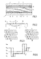
- Fig. 1 shows in a diagrammatic cross-section a part of a display device, in this embodiment a liquid crystal display device 1, comprising two supporting plates 2 and 3 between which, for example, a twisted nematic liquid crystalline material 4 is present.
- the inner surfaces of the supporting plates 2 and 3 are provided with electrically and chemically insulating layers 5.
- a number of row and column-arranged picture electrodes 6 of indium-tin oxide or another electrically conducting transparent material is provided on the supporting plate 2.
- Transparent picture electrodes 7 of, for example, indium-tin oxide which are integrated to strip-shaped electrodes (in this embodiment column electrodes) are also provided on the supporting plate 3.
- the facing picture electrodes 6, 7 constitute the pixels of the display device.
- Strip-shaped (for example, metal) row electrodes 8 are arranged between the rows of picture electrodes 6. Each picture electrode 6 is connected to a row electrode 8 via a switching element (not shown). Furthermore, liquid crystal orienting layers 10, 18 are provided on the inner surfaces of the supporting plates 2 and 3. As is known, a different orientation state of the liquid crystal molecules and hence an optically different state can be obtained by applying a voltage across the liquid crystal layer 4.
- the display device can be realised as a transmissive or a reflective device and may have one or two polarizers.
- a stray capacitance C c which is diagrammatically illustrated by means of the field line 9, is produced via the substrate 2 of, for example, glass.
- the picture electrode 6a associated with the first pixel 11a receives a voltage of, for example, -V c after selection. If the picture electrode 6 b associated with the next pixel also receives a voltage -V c in a subsequent selection period after it has received a voltage of +V c in a previous (frame or field) period (the transmission value of juxtaposed pixels, notably in large areas, is often closely correlated), the voltage across the picture electrode 6 b changes from +V c to -V c .
- Cp is the capacitance of the pixel and C m is the capacitance of the non-linear switching element (see also Fig. 5).
- the absolute value of the voltage across the first picture electrode increases when the second picture electrode is charged in the same direction and the first pixel becomes darker (based on a twisted nematic liquid crystal effect between crossed polarizers).
- Fig. 3a is a diagrammatic plan view of a plurality of pixels 11 of a colour display device with a colour filter whose colour elements (corresponding to pixels) in juxtaposed rows are shifted with respect to each other over half a pitch.
- a colour filter whose colour elements (corresponding to pixels) in juxtaposed rows are shifted with respect to each other over half a pitch.
- the display device shown in this Figure comprises a plurality of pixels 11 arranged in rows and columns which are driven via switching elements 12, for example, MIMs (metal-isolator-metal)-.By successively selecting (energizing) row electrodes 8, information which is present on the column electrodes 7 is presented to the pixels 11.
- Row electrodes 8 are consecutively selected by means of, for example, a row selection circuit 13, while the information to be presented for a selected row of pixels is stored in a register 15.
- the assembly is driven and synchronized by means of the switching unit 15.
- the rows are divided into groups of two, with the possible exception of the first and the last row, i.e. a display device comprising n rows of pixels is then divided into at least (n-2)/2 groups of two rows of pixels.
- Fig. 5a shows a part (three pixels) of the device of Fig. 4 in which the stray capacitance C c is shown by means of broken lines. If the pixels 11° and 11 are consecutively charged positively (double line inversion) by means of selection voltages on the row electrodes 8a, 8 b and if subsequently pixel 11° is charged negatively by selecting row electrode 8°, the voltage across pixel 11 is decreased. According to the invention this is prevented by choosing the selection voltage across the row electrode 8a (hence 8° ...) to be lower, or by choosing the voltage across the row electrode 8 b to be higher; a combination is alternatively possible. In the relevant embodiment in which the row electrodes are divided into groups of two the selection voltages within each group of two are thus different.
- the correction to be set is also dependent on the setting on the transmission/voltage characteristic curve and is preferably set at a value halfway this characteristic curve (medium grey).
- Fig. 4 can also be driven by means of the method as described in EP-A-0 362 939 (PHN 12.698) which is herein incorporated by reference.
- the invention is of course not limited to the embodiments described but several variations are possible within the scope of the invention.
- the stray capacitance which causes said capacitive coupling between the rows, does not only exist in devices with two-poles as shown in the Figures but also in active pixels based on three-poles such as TFTs so that the invention is also applicable in this field.
- the stray capacitance to a picture electrode which is further remote may be taken into account, if necessary, in the adaptation of the selection voltages.
Landscapes
- Engineering & Computer Science (AREA)
- Chemical & Material Sciences (AREA)
- Crystallography & Structural Chemistry (AREA)
- Physics & Mathematics (AREA)
- Computer Hardware Design (AREA)
- General Physics & Mathematics (AREA)
- Theoretical Computer Science (AREA)
- Liquid Crystal Display Device Control (AREA)
- Control Of Indicators Other Than Cathode Ray Tubes (AREA)
- Liquid Crystal (AREA)
Applications Claiming Priority (2)
| Application Number | Priority Date | Filing Date | Title |
|---|---|---|---|
| EP91201789 | 1991-07-09 | ||
| EP91201789 | 1991-09-07 |
Publications (2)
| Publication Number | Publication Date |
|---|---|
| EP0525852A1 true EP0525852A1 (fr) | 1993-02-03 |
| EP0525852B1 EP0525852B1 (fr) | 1996-05-22 |
Family
ID=8207770
Family Applications (1)
| Application Number | Title | Priority Date | Filing Date |
|---|---|---|---|
| EP92201992A Expired - Lifetime EP0525852B1 (fr) | 1991-07-09 | 1992-07-02 | Dispositif de reproduction |
Country Status (4)
| Country | Link |
|---|---|
| US (1) | US5689282A (fr) |
| EP (1) | EP0525852B1 (fr) |
| JP (1) | JPH05216429A (fr) |
| DE (1) | DE69210904T2 (fr) |
Cited By (27)
| Publication number | Priority date | Publication date | Assignee | Title |
|---|---|---|---|---|
| FR2707788A1 (fr) * | 1993-07-12 | 1995-01-20 | Motorola Inc | Procédé et appareil pour réduire les discontinuités dans un système d'affichage à adressage actif. |
| US6177921B1 (en) | 1997-08-28 | 2001-01-23 | E Ink Corporation | Printable electrode structures for displays |
| US6323989B1 (en) | 1996-07-19 | 2001-11-27 | E Ink Corporation | Electrophoretic displays using nanoparticles |
| WO2001091096A1 (fr) * | 2000-05-26 | 2001-11-29 | Seiko Epson Corporation | Unite d'affichage et support enregistre |
| US6422687B1 (en) | 1996-07-19 | 2002-07-23 | E Ink Corporation | Electronically addressable microencapsulated ink and display thereof |
| US6445489B1 (en) * | 1998-03-18 | 2002-09-03 | E Ink Corporation | Electrophoretic displays and systems for addressing such displays |
| US6445374B2 (en) | 1997-08-28 | 2002-09-03 | E Ink Corporation | Rear electrode structures for displays |
| US6538801B2 (en) | 1996-07-19 | 2003-03-25 | E Ink Corporation | Electrophoretic displays using nanoparticles |
| US6664944B1 (en) | 1995-07-20 | 2003-12-16 | E-Ink Corporation | Rear electrode structures for electrophoretic displays |
| US6710540B1 (en) | 1995-07-20 | 2004-03-23 | E Ink Corporation | Electrostatically-addressable electrophoretic display |
| US6724519B1 (en) | 1998-12-21 | 2004-04-20 | E-Ink Corporation | Protective electrodes for electrophoretic displays |
| US6727881B1 (en) | 1995-07-20 | 2004-04-27 | E Ink Corporation | Encapsulated electrophoretic displays and methods and materials for making the same |
| US6825068B2 (en) | 2000-04-18 | 2004-11-30 | E Ink Corporation | Process for fabricating thin film transistors |
| US6839158B2 (en) | 1997-08-28 | 2005-01-04 | E Ink Corporation | Encapsulated electrophoretic displays having a monolayer of capsules and materials and methods for making the same |
| US6865010B2 (en) | 2001-12-13 | 2005-03-08 | E Ink Corporation | Electrophoretic electronic displays with low-index films |
| US6864875B2 (en) | 1998-04-10 | 2005-03-08 | E Ink Corporation | Full color reflective display with multichromatic sub-pixels |
| US6900851B2 (en) | 2002-02-08 | 2005-05-31 | E Ink Corporation | Electro-optic displays and optical systems for addressing such displays |
| US6967640B2 (en) | 2001-07-27 | 2005-11-22 | E Ink Corporation | Microencapsulated electrophoretic display with integrated driver |
| US7030412B1 (en) | 1999-05-05 | 2006-04-18 | E Ink Corporation | Minimally-patterned semiconductor devices for display applications |
| US7038655B2 (en) | 1999-05-03 | 2006-05-02 | E Ink Corporation | Electrophoretic ink composed of particles with field dependent mobilities |
| US7071913B2 (en) | 1995-07-20 | 2006-07-04 | E Ink Corporation | Retroreflective electrophoretic displays and materials for making the same |
| US7109968B2 (en) | 1995-07-20 | 2006-09-19 | E Ink Corporation | Non-spherical cavity electrophoretic displays and methods and materials for making the same |
| US7167155B1 (en) | 1995-07-20 | 2007-01-23 | E Ink Corporation | Color electrophoretic displays |
| US7256766B2 (en) | 1998-08-27 | 2007-08-14 | E Ink Corporation | Electrophoretic display comprising optical biasing element |
| US7304634B2 (en) | 1995-07-20 | 2007-12-04 | E Ink Corporation | Rear electrode structures for electrophoretic displays |
| US7352353B2 (en) | 1995-07-20 | 2008-04-01 | E Ink Corporation | Electrostatically addressable electrophoretic display |
| US7667684B2 (en) | 1998-07-08 | 2010-02-23 | E Ink Corporation | Methods for achieving improved color in microencapsulated electrophoretic devices |
Families Citing this family (59)
| Publication number | Priority date | Publication date | Assignee | Title |
|---|---|---|---|---|
| US7193625B2 (en) | 1999-04-30 | 2007-03-20 | E Ink Corporation | Methods for driving electro-optic displays, and apparatus for use therein |
| US7956841B2 (en) | 1995-07-20 | 2011-06-07 | E Ink Corporation | Stylus-based addressing structures for displays |
| US6017584A (en) * | 1995-07-20 | 2000-01-25 | E Ink Corporation | Multi-color electrophoretic displays and materials for making the same |
| US8089453B2 (en) * | 1995-07-20 | 2012-01-03 | E Ink Corporation | Stylus-based addressing structures for displays |
| US8139050B2 (en) | 1995-07-20 | 2012-03-20 | E Ink Corporation | Addressing schemes for electronic displays |
| US7999787B2 (en) | 1995-07-20 | 2011-08-16 | E Ink Corporation | Methods for driving electrophoretic displays using dielectrophoretic forces |
| US6515649B1 (en) | 1995-07-20 | 2003-02-04 | E Ink Corporation | Suspended particle displays and materials for making the same |
| EP1231500B1 (fr) * | 1996-07-19 | 2007-03-07 | E-Ink Corporation | Encre micro-encapsulée adressable électroniquement |
| US6067185A (en) | 1997-08-28 | 2000-05-23 | E Ink Corporation | Process for creating an encapsulated electrophoretic display |
| US8040594B2 (en) | 1997-08-28 | 2011-10-18 | E Ink Corporation | Multi-color electrophoretic displays |
| US7247379B2 (en) | 1997-08-28 | 2007-07-24 | E Ink Corporation | Electrophoretic particles, and processes for the production thereof |
| US7002728B2 (en) | 1997-08-28 | 2006-02-21 | E Ink Corporation | Electrophoretic particles, and processes for the production thereof |
| US7242513B2 (en) | 1997-08-28 | 2007-07-10 | E Ink Corporation | Encapsulated electrophoretic displays having a monolayer of capsules and materials and methods for making the same |
| US8213076B2 (en) | 1997-08-28 | 2012-07-03 | E Ink Corporation | Multi-color electrophoretic displays and materials for making the same |
| US6704133B2 (en) | 1998-03-18 | 2004-03-09 | E-Ink Corporation | Electro-optic display overlays and systems for addressing such displays |
| AU3552699A (en) | 1998-04-10 | 1999-11-01 | E-Ink Corporation | Electronic displays using organic-based field effect transistors |
| AU3987299A (en) | 1998-05-12 | 1999-11-29 | E-Ink Corporation | Microencapsulated electrophoretic electrostatically-addressed media for drawing device applications |
| WO2000020923A1 (fr) | 1998-10-07 | 2000-04-13 | E Ink Corporation | Systeme d'eclairage pour afficheurs electroniques non emissifs |
| US6312304B1 (en) | 1998-12-15 | 2001-11-06 | E Ink Corporation | Assembly of microencapsulated electronic displays |
| WO2000059625A1 (fr) | 1999-04-06 | 2000-10-12 | E Ink Corporation | Procedes de production de gouttelettes destines a des afficheurs par electrophorese encapsules |
| US6498114B1 (en) | 1999-04-09 | 2002-12-24 | E Ink Corporation | Method for forming a patterned semiconductor film |
| US6842657B1 (en) | 1999-04-09 | 2005-01-11 | E Ink Corporation | Reactive formation of dielectric layers and protection of organic layers in organic semiconductor device fabrication |
| US7012600B2 (en) | 1999-04-30 | 2006-03-14 | E Ink Corporation | Methods for driving bistable electro-optic displays, and apparatus for use therein |
| US7119772B2 (en) | 1999-04-30 | 2006-10-10 | E Ink Corporation | Methods for driving bistable electro-optic displays, and apparatus for use therein |
| US6531997B1 (en) | 1999-04-30 | 2003-03-11 | E Ink Corporation | Methods for addressing electrophoretic displays |
| US6504524B1 (en) | 2000-03-08 | 2003-01-07 | E Ink Corporation | Addressing methods for displays having zero time-average field |
| US6693620B1 (en) | 1999-05-03 | 2004-02-17 | E Ink Corporation | Threshold addressing of electrophoretic displays |
| US8115729B2 (en) | 1999-05-03 | 2012-02-14 | E Ink Corporation | Electrophoretic display element with filler particles |
| AU6365900A (en) | 1999-07-21 | 2001-02-13 | E-Ink Corporation | Use of a storage capacitor to enhance the performance of an active matrix drivenelectronic display |
| US7893435B2 (en) | 2000-04-18 | 2011-02-22 | E Ink Corporation | Flexible electronic circuits and displays including a backplane comprising a patterned metal foil having a plurality of apertures extending therethrough |
| US20020060321A1 (en) | 2000-07-14 | 2002-05-23 | Kazlas Peter T. | Minimally- patterned, thin-film semiconductor devices for display applications |
| JP2002055661A (ja) * | 2000-08-11 | 2002-02-20 | Nec Corp | 液晶ディスプレイの駆動方法、その回路及び画像表示装置 |
| AU2002230520A1 (en) * | 2000-11-29 | 2002-06-11 | E-Ink Corporation | Addressing circuitry for large electronic displays |
| US7230750B2 (en) | 2001-05-15 | 2007-06-12 | E Ink Corporation | Electrophoretic media and processes for the production thereof |
| KR100767364B1 (ko) * | 2001-06-19 | 2007-10-17 | 삼성전자주식회사 | 액정 표시 장치 및 그 구동 방법 |
| US8125501B2 (en) | 2001-11-20 | 2012-02-28 | E Ink Corporation | Voltage modulated driver circuits for electro-optic displays |
| US8558783B2 (en) | 2001-11-20 | 2013-10-15 | E Ink Corporation | Electro-optic displays with reduced remnant voltage |
| US8593396B2 (en) | 2001-11-20 | 2013-11-26 | E Ink Corporation | Methods and apparatus for driving electro-optic displays |
| US7952557B2 (en) | 2001-11-20 | 2011-05-31 | E Ink Corporation | Methods and apparatus for driving electro-optic displays |
| US7528822B2 (en) | 2001-11-20 | 2009-05-05 | E Ink Corporation | Methods for driving electro-optic displays |
| US9412314B2 (en) | 2001-11-20 | 2016-08-09 | E Ink Corporation | Methods for driving electro-optic displays |
| US9530363B2 (en) | 2001-11-20 | 2016-12-27 | E Ink Corporation | Methods and apparatus for driving electro-optic displays |
| KR100870006B1 (ko) * | 2002-05-27 | 2008-11-21 | 삼성전자주식회사 | 액정 표시 장치 및 그 구동 방법 |
| US20080024482A1 (en) | 2002-06-13 | 2008-01-31 | E Ink Corporation | Methods for driving electro-optic displays |
| US7312916B2 (en) | 2002-08-07 | 2007-12-25 | E Ink Corporation | Electrophoretic media containing specularly reflective particles |
| US20130063333A1 (en) | 2002-10-16 | 2013-03-14 | E Ink Corporation | Electrophoretic displays |
| US10726798B2 (en) | 2003-03-31 | 2020-07-28 | E Ink Corporation | Methods for operating electro-optic displays |
| US8174490B2 (en) | 2003-06-30 | 2012-05-08 | E Ink Corporation | Methods for driving electrophoretic displays |
| KR20060080869A (ko) * | 2003-07-04 | 2006-07-11 | 코닌클리케 필립스 일렉트로닉스 엔.브이. | 전기영동 디스플레이 패널 |
| US7034783B2 (en) | 2003-08-19 | 2006-04-25 | E Ink Corporation | Method for controlling electro-optic display |
| US8928562B2 (en) | 2003-11-25 | 2015-01-06 | E Ink Corporation | Electro-optic displays, and methods for driving same |
| US7492339B2 (en) | 2004-03-26 | 2009-02-17 | E Ink Corporation | Methods for driving bistable electro-optic displays |
| US11250794B2 (en) | 2004-07-27 | 2022-02-15 | E Ink Corporation | Methods for driving electrophoretic displays using dielectrophoretic forces |
| US7453445B2 (en) | 2004-08-13 | 2008-11-18 | E Ink Corproation | Methods for driving electro-optic displays |
| JP4329780B2 (ja) * | 2006-05-01 | 2009-09-09 | セイコーエプソン株式会社 | 液晶装置の駆動方法及び液晶装置並びに電子機器 |
| US8089687B2 (en) * | 2009-12-21 | 2012-01-03 | Hewlett-Packard Development Company, L.P. | Electro-optical display systems |
| US7957054B1 (en) | 2009-12-21 | 2011-06-07 | Hewlett-Packard Development Company, L.P. | Electro-optical display systems |
| CN105654889B (zh) | 2010-04-09 | 2022-01-11 | 伊英克公司 | 用于驱动电光显示器的方法 |
| TWI484275B (zh) | 2010-05-21 | 2015-05-11 | E Ink Corp | 光電顯示器及其驅動方法、微型空腔電泳顯示器 |
Citations (2)
| Publication number | Priority date | Publication date | Assignee | Title |
|---|---|---|---|---|
| EP0295802A1 (fr) * | 1987-05-29 | 1988-12-21 | Sharp Kabushiki Kaisha | Dispositif d'affichage à cristaux liquides |
| EP0479552A2 (fr) * | 1990-10-01 | 1992-04-08 | Sharp Kabushiki Kaisha | Dispositif d'affichage |
Family Cites Families (4)
| Publication number | Priority date | Publication date | Assignee | Title |
|---|---|---|---|---|
| JPS5576393A (en) * | 1978-12-04 | 1980-06-09 | Hitachi Ltd | Matrix drive method for guestthostttype phase transfer liquid crystal |
| JPH07118794B2 (ja) * | 1983-03-16 | 1995-12-18 | シチズン時計株式会社 | 表示装置 |
| JPS60218626A (ja) * | 1984-04-13 | 1985-11-01 | Sharp Corp | カラ−液晶表示装置 |
| WO1986001624A1 (fr) * | 1984-08-23 | 1986-03-13 | Sony Corporation | Affichage a cristaux liquides |
-
1992
- 1992-06-15 US US07/898,985 patent/US5689282A/en not_active Expired - Fee Related
- 1992-07-02 EP EP92201992A patent/EP0525852B1/fr not_active Expired - Lifetime
- 1992-07-02 DE DE69210904T patent/DE69210904T2/de not_active Expired - Fee Related
- 1992-07-09 JP JP4182507A patent/JPH05216429A/ja active Pending
Patent Citations (2)
| Publication number | Priority date | Publication date | Assignee | Title |
|---|---|---|---|---|
| EP0295802A1 (fr) * | 1987-05-29 | 1988-12-21 | Sharp Kabushiki Kaisha | Dispositif d'affichage à cristaux liquides |
| EP0479552A2 (fr) * | 1990-10-01 | 1992-04-08 | Sharp Kabushiki Kaisha | Dispositif d'affichage |
Non-Patent Citations (1)
| Title |
|---|
| KOHDA S., ET AL.: "A DEFECT-TOLERANT ACTIVE-MATRIX CIRCUIT AND ITS APPLICATION TO A HIGH-RESOLUTION COLOR LCD.", PROCEEDINGS OF THE SOCIETY OF INFORMATION DISPLAY, SOCIETY FOR INFORMATION DISPLAY. PLAYA DEL REY, CA., US, vol. 30., no. 03., 1 January 1989 (1989-01-01), US, pages 259 - 262., XP000115848 * |
Cited By (36)
| Publication number | Priority date | Publication date | Assignee | Title |
|---|---|---|---|---|
| NL9401151A (nl) * | 1993-07-12 | 1995-02-01 | Motorola Inc | Werkwijze en inrichting voor het reduceren van discontinuiteiten in een weergeefsysteem met actieve adressering. |
| FR2707788A1 (fr) * | 1993-07-12 | 1995-01-20 | Motorola Inc | Procédé et appareil pour réduire les discontinuités dans un système d'affichage à adressage actif. |
| US6710540B1 (en) | 1995-07-20 | 2004-03-23 | E Ink Corporation | Electrostatically-addressable electrophoretic display |
| US8593718B2 (en) | 1995-07-20 | 2013-11-26 | E Ink Corporation | Electro-osmotic displays and materials for making the same |
| US7746544B2 (en) | 1995-07-20 | 2010-06-29 | E Ink Corporation | Electro-osmotic displays and materials for making the same |
| US7352353B2 (en) | 1995-07-20 | 2008-04-01 | E Ink Corporation | Electrostatically addressable electrophoretic display |
| US7304634B2 (en) | 1995-07-20 | 2007-12-04 | E Ink Corporation | Rear electrode structures for electrophoretic displays |
| US7167155B1 (en) | 1995-07-20 | 2007-01-23 | E Ink Corporation | Color electrophoretic displays |
| US7109968B2 (en) | 1995-07-20 | 2006-09-19 | E Ink Corporation | Non-spherical cavity electrophoretic displays and methods and materials for making the same |
| US7071913B2 (en) | 1995-07-20 | 2006-07-04 | E Ink Corporation | Retroreflective electrophoretic displays and materials for making the same |
| US6727881B1 (en) | 1995-07-20 | 2004-04-27 | E Ink Corporation | Encapsulated electrophoretic displays and methods and materials for making the same |
| US6664944B1 (en) | 1995-07-20 | 2003-12-16 | E-Ink Corporation | Rear electrode structures for electrophoretic displays |
| US6538801B2 (en) | 1996-07-19 | 2003-03-25 | E Ink Corporation | Electrophoretic displays using nanoparticles |
| US6323989B1 (en) | 1996-07-19 | 2001-11-27 | E Ink Corporation | Electrophoretic displays using nanoparticles |
| US6652075B2 (en) | 1996-07-19 | 2003-11-25 | E Ink Corporation | Electronically addressable microencapsulated ink and display thereof |
| US6422687B1 (en) | 1996-07-19 | 2002-07-23 | E Ink Corporation | Electronically addressable microencapsulated ink and display thereof |
| US6535197B1 (en) | 1997-08-28 | 2003-03-18 | E Ink Corporation | Printable electrode structures for displays |
| US6842167B2 (en) | 1997-08-28 | 2005-01-11 | E Ink Corporation | Rear electrode structures for displays |
| US6839158B2 (en) | 1997-08-28 | 2005-01-04 | E Ink Corporation | Encapsulated electrophoretic displays having a monolayer of capsules and materials and methods for making the same |
| US6177921B1 (en) | 1997-08-28 | 2001-01-23 | E Ink Corporation | Printable electrode structures for displays |
| US6445374B2 (en) | 1997-08-28 | 2002-09-03 | E Ink Corporation | Rear electrode structures for displays |
| US6445489B1 (en) * | 1998-03-18 | 2002-09-03 | E Ink Corporation | Electrophoretic displays and systems for addressing such displays |
| US8466852B2 (en) | 1998-04-10 | 2013-06-18 | E Ink Corporation | Full color reflective display with multichromatic sub-pixels |
| US6864875B2 (en) | 1998-04-10 | 2005-03-08 | E Ink Corporation | Full color reflective display with multichromatic sub-pixels |
| US7075502B1 (en) | 1998-04-10 | 2006-07-11 | E Ink Corporation | Full color reflective display with multichromatic sub-pixels |
| US7667684B2 (en) | 1998-07-08 | 2010-02-23 | E Ink Corporation | Methods for achieving improved color in microencapsulated electrophoretic devices |
| US7256766B2 (en) | 1998-08-27 | 2007-08-14 | E Ink Corporation | Electrophoretic display comprising optical biasing element |
| US6724519B1 (en) | 1998-12-21 | 2004-04-20 | E-Ink Corporation | Protective electrodes for electrophoretic displays |
| US7038655B2 (en) | 1999-05-03 | 2006-05-02 | E Ink Corporation | Electrophoretic ink composed of particles with field dependent mobilities |
| US7030412B1 (en) | 1999-05-05 | 2006-04-18 | E Ink Corporation | Minimally-patterned semiconductor devices for display applications |
| US6825068B2 (en) | 2000-04-18 | 2004-11-30 | E Ink Corporation | Process for fabricating thin film transistors |
| WO2001091096A1 (fr) * | 2000-05-26 | 2001-11-29 | Seiko Epson Corporation | Unite d'affichage et support enregistre |
| US6842165B2 (en) | 2000-05-26 | 2005-01-11 | Seiko Epson Corporation | Display device and recording medium |
| US6967640B2 (en) | 2001-07-27 | 2005-11-22 | E Ink Corporation | Microencapsulated electrophoretic display with integrated driver |
| US6865010B2 (en) | 2001-12-13 | 2005-03-08 | E Ink Corporation | Electrophoretic electronic displays with low-index films |
| US6900851B2 (en) | 2002-02-08 | 2005-05-31 | E Ink Corporation | Electro-optic displays and optical systems for addressing such displays |
Also Published As
| Publication number | Publication date |
|---|---|
| EP0525852B1 (fr) | 1996-05-22 |
| DE69210904T2 (de) | 1996-11-28 |
| DE69210904D1 (de) | 1996-06-27 |
| JPH05216429A (ja) | 1993-08-27 |
| US5689282A (en) | 1997-11-18 |
Similar Documents
| Publication | Publication Date | Title |
|---|---|---|
| EP0525852B1 (fr) | Dispositif de reproduction | |
| USRE37906E1 (en) | Display device and method of driving such a device | |
| EP0284134B1 (fr) | Méthode de commande d'un dispositif d'affichage à cristal liquide et dispositif d'affichage associé | |
| US5898416A (en) | Display device | |
| EP0244013B1 (fr) | Dispositif d'affichage en couleurs | |
| KR100788392B1 (ko) | 횡전계 방식 액정 표시 장치의 구동방법 | |
| US7109963B2 (en) | Display device | |
| US6313818B1 (en) | Adjustment method for active-matrix type liquid crystal display device | |
| AU601375B2 (en) | Display arrangement with improved drive | |
| JP2505826B2 (ja) | デイスプレイ装置 | |
| US4994796A (en) | Electro optical display device with redundant switching means | |
| US6052104A (en) | Structure and operation method of LCD | |
| JPH04269792A (ja) | マトリクス表示装置の駆動方法及びこの方法で動作し得るマトリクス表示装置 | |
| KR960007476B1 (ko) | 디스플레이 장치 및 그 구동 방법 | |
| US5032830A (en) | Electro-optical display device with non-linear switching units with auxiliary voltages and capacitively coupled row electrodes | |
| KR100482160B1 (ko) | 액정표시장치용 어레이기판 | |
| US5742270A (en) | Over line scan method | |
| KR100965587B1 (ko) | 액정표시장치 및 이의 구동방법 | |
| JPH0635417A (ja) | アクティブマトリクス型薄膜トランジスタ液晶パネルの駆動方法 | |
| WO1996016392A1 (fr) | Circuit de correction destine a compenser des changements de parametres dans un affichage a matrice active |
Legal Events
| Date | Code | Title | Description |
|---|---|---|---|
| PUAI | Public reference made under article 153(3) epc to a published international application that has entered the european phase |
Free format text: ORIGINAL CODE: 0009012 |
|
| AK | Designated contracting states |
Kind code of ref document: A1 Designated state(s): DE FR GB IT NL |
|
| 17P | Request for examination filed |
Effective date: 19930719 |
|
| 17Q | First examination report despatched |
Effective date: 19950623 |
|
| GRAH | Despatch of communication of intention to grant a patent |
Free format text: ORIGINAL CODE: EPIDOS IGRA |
|
| GRAA | (expected) grant |
Free format text: ORIGINAL CODE: 0009210 |
|
| AK | Designated contracting states |
Kind code of ref document: B1 Designated state(s): DE FR GB IT NL |
|
| PG25 | Lapsed in a contracting state [announced via postgrant information from national office to epo] |
Ref country code: IT Free format text: LAPSE BECAUSE OF FAILURE TO SUBMIT A TRANSLATION OF THE DESCRIPTION OR TO PAY THE FEE WITHIN THE PRESCRIBED TIME-LIMIT;WARNING: LAPSES OF ITALIAN PATENTS WITH EFFECTIVE DATE BEFORE 2007 MAY HAVE OCCURRED AT ANY TIME BEFORE 2007. THE CORRECT EFFECTIVE DATE MAY BE DIFFERENT FROM THE ONE RECORDED. Effective date: 19960522 Ref country code: NL Free format text: LAPSE BECAUSE OF FAILURE TO SUBMIT A TRANSLATION OF THE DESCRIPTION OR TO PAY THE FEE WITHIN THE PRESCRIBED TIME-LIMIT Effective date: 19960522 |
|
| REF | Corresponds to: |
Ref document number: 69210904 Country of ref document: DE Date of ref document: 19960627 |
|
| ET | Fr: translation filed | ||
| NLV1 | Nl: lapsed or annulled due to failure to fulfill the requirements of art. 29p and 29m of the patents act | ||
| PLBE | No opposition filed within time limit |
Free format text: ORIGINAL CODE: 0009261 |
|
| STAA | Information on the status of an ep patent application or granted ep patent |
Free format text: STATUS: NO OPPOSITION FILED WITHIN TIME LIMIT |
|
| 26N | No opposition filed | ||
| PGFP | Annual fee paid to national office [announced via postgrant information from national office to epo] |
Ref country code: GB Payment date: 19970701 Year of fee payment: 6 |
|
| PGFP | Annual fee paid to national office [announced via postgrant information from national office to epo] |
Ref country code: FR Payment date: 19970722 Year of fee payment: 6 |
|
| PG25 | Lapsed in a contracting state [announced via postgrant information from national office to epo] |
Ref country code: GB Free format text: LAPSE BECAUSE OF NON-PAYMENT OF DUE FEES Effective date: 19980702 |
|
| REG | Reference to a national code |
Ref country code: FR Ref legal event code: CD |
|
| GBPC | Gb: european patent ceased through non-payment of renewal fee |
Effective date: 19980702 |
|
| PG25 | Lapsed in a contracting state [announced via postgrant information from national office to epo] |
Ref country code: FR Free format text: LAPSE BECAUSE OF NON-PAYMENT OF DUE FEES Effective date: 19990331 |
|
| REG | Reference to a national code |
Ref country code: FR Ref legal event code: ST |
|
| PGFP | Annual fee paid to national office [announced via postgrant information from national office to epo] |
Ref country code: DE Payment date: 19990826 Year of fee payment: 8 |
|
| PG25 | Lapsed in a contracting state [announced via postgrant information from national office to epo] |
Ref country code: DE Free format text: LAPSE BECAUSE OF NON-PAYMENT OF DUE FEES Effective date: 20010501 |