EP0525876A1 - Détecteurs infrarouges - Google Patents
Détecteurs infrarouges Download PDFInfo
- Publication number
- EP0525876A1 EP0525876A1 EP92202222A EP92202222A EP0525876A1 EP 0525876 A1 EP0525876 A1 EP 0525876A1 EP 92202222 A EP92202222 A EP 92202222A EP 92202222 A EP92202222 A EP 92202222A EP 0525876 A1 EP0525876 A1 EP 0525876A1
- Authority
- EP
- European Patent Office
- Prior art keywords
- layer
- detector
- substrate
- infrared
- further characterised
- Prior art date
- Legal status (The legal status is an assumption and is not a legal conclusion. Google has not performed a legal analysis and makes no representation as to the accuracy of the status listed.)
- Granted
Links
Images


Classifications
-
- H—ELECTRICITY
- H10—SEMICONDUCTOR DEVICES; ELECTRIC SOLID-STATE DEVICES NOT OTHERWISE PROVIDED FOR
- H10F—INORGANIC SEMICONDUCTOR DEVICES SENSITIVE TO INFRARED RADIATION, LIGHT, ELECTROMAGNETIC RADIATION OF SHORTER WAVELENGTH OR CORPUSCULAR RADIATION
- H10F39/00—Integrated devices, or assemblies of multiple devices, comprising at least one element covered by group H10F30/00, e.g. radiation detectors comprising photodiode arrays
- H10F39/10—Integrated devices
- H10F39/12—Image sensors
- H10F39/18—Complementary metal-oxide-semiconductor [CMOS] image sensors; Photodiode array image sensors
- H10F39/184—Infrared image sensors
-
- H—ELECTRICITY
- H10—SEMICONDUCTOR DEVICES; ELECTRIC SOLID-STATE DEVICES NOT OTHERWISE PROVIDED FOR
- H10F—INORGANIC SEMICONDUCTOR DEVICES SENSITIVE TO INFRARED RADIATION, LIGHT, ELECTROMAGNETIC RADIATION OF SHORTER WAVELENGTH OR CORPUSCULAR RADIATION
- H10F39/00—Integrated devices, or assemblies of multiple devices, comprising at least one element covered by group H10F30/00, e.g. radiation detectors comprising photodiode arrays
- H10F39/80—Constructional details of image sensors
- H10F39/806—Optical elements or arrangements associated with the image sensors
- H10F39/8063—Microlenses
-
- H—ELECTRICITY
- H10—SEMICONDUCTOR DEVICES; ELECTRIC SOLID-STATE DEVICES NOT OTHERWISE PROVIDED FOR
- H10F—INORGANIC SEMICONDUCTOR DEVICES SENSITIVE TO INFRARED RADIATION, LIGHT, ELECTROMAGNETIC RADIATION OF SHORTER WAVELENGTH OR CORPUSCULAR RADIATION
- H10F77/00—Constructional details of devices covered by this subclass
- H10F77/10—Semiconductor bodies
- H10F77/14—Shape of semiconductor bodies; Shapes, relative sizes or dispositions of semiconductor regions within semiconductor bodies
- H10F77/147—Shapes of bodies
-
- H—ELECTRICITY
- H10—SEMICONDUCTOR DEVICES; ELECTRIC SOLID-STATE DEVICES NOT OTHERWISE PROVIDED FOR
- H10F—INORGANIC SEMICONDUCTOR DEVICES SENSITIVE TO INFRARED RADIATION, LIGHT, ELECTROMAGNETIC RADIATION OF SHORTER WAVELENGTH OR CORPUSCULAR RADIATION
- H10F77/00—Constructional details of devices covered by this subclass
- H10F77/40—Optical elements or arrangements
- H10F77/413—Optical elements or arrangements directly associated or integrated with the devices, e.g. back reflectors
-
- Y—GENERAL TAGGING OF NEW TECHNOLOGICAL DEVELOPMENTS; GENERAL TAGGING OF CROSS-SECTIONAL TECHNOLOGIES SPANNING OVER SEVERAL SECTIONS OF THE IPC; TECHNICAL SUBJECTS COVERED BY FORMER USPC CROSS-REFERENCE ART COLLECTIONS [XRACs] AND DIGESTS
- Y02—TECHNOLOGIES OR APPLICATIONS FOR MITIGATION OR ADAPTATION AGAINST CLIMATE CHANGE
- Y02E—REDUCTION OF GREENHOUSE GAS [GHG] EMISSIONS, RELATED TO ENERGY GENERATION, TRANSMISSION OR DISTRIBUTION
- Y02E10/00—Energy generation through renewable energy sources
- Y02E10/50—Photovoltaic [PV] energy
Definitions
- This invention relates to infrared detectors comprising at least one detector element sandwiched between a substrate and an optical element, and relates particularly but not exclusively to such infrared detectors comprising an array of detector elements of cadmium mercury telluride with a corresponding array of immersion lenses as the optical element.
- an infrared detector comprising a detector element which has a body of infrared-sensitive semiconductor material (for example, cadmium mercury telluride) and which is sandwiched between a substrate and an optical element in the form of a lens, the lens being secured over the element body by an adhesive film.
- infrared-sensitive semiconductor material for example, cadmium mercury telluride
- GB-A-2 132 757 the adhesive film is present between the detector element and the lens so as to bond the detector element to the lens.
- its presence was considered in GB-A-2 132 757 to give rise to difficulties in infrared transmission through the adhesive, in differential thermal expansion leading to structural failure and in adversely affecting a passivated surface of the element body.
- the invention disclosed in GB-A-2 132 757 provides three small radially-disposed lens contact pads around a single detector element and avoids the provision of the adhesive film between the detector element and the lens.
- the adhesive film is provided only on the three radially-disposed contact pads which are formed of the same material as the element body.
- Immersion lenses and other optical concentrators have also been formed as an array in an optical plate as described in United Kingdom patent specification GB-A-1 525 562, the whole contents of which are hereby incorporated herein as reference material. Similar arrays have also been formed in an optical plate for infrared regions of the spectrum, for example the wavebands 3 to 5 ⁇ m (micrometers) and 8 to 14 /1 .m.
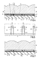
- Pending United Kingdom patent application (GB) 8522539 our reference PHB33199) of 11th September 1985 (published as GB-A-2 241 605 on 4th September 1991) describes an array of infrared detector elements (for example of cadmium mercury telluride) which is bonded to such a lens-array plate by an adhesive film. Such an arrangement is illustrated in Figures 1 and 2 of the accompanying drawings.
- the adhesive film 11 extends between the element bodies 1 and the lens plate 10 and fills the space between the element bodies 1.
- the detector elements are infrared photodiodes having a vertical p-n junction 3 dividing the body into a p type region 2 and an n type region 4.
- the element bodies 1 are mounted (for example by a further adhesive film, not shown in the drawings) on a substrate 20 carrying electrical connections 22 and 24 to respective electrodes 5 and 6 of the regions 2 and 4.
- Figure 3 is a graph illustrating the shift in the cut-off wavelength X in /1.m.
- the reciprocal of X is plotted as the ordinate against the operating temperature T of the detector element in degrees Kelvin as the abscissa.
- the line A is for the detector element material without the lens plate 10 bonded thereto, whereas line B is for the bonded element structure of Figures 1 and 2 with a silicon lens array 10 and an epoxy adhesive film 11.
- an infrared detector comprising at least one detector element which has a body of infrared-sensitive semiconductor material and which is sandwiched between two members, namely a substrate and an optical element, one of the members being secured over the body by an adhesive film, which device is characterised in that the element body is a part of a wider layer of the infrared-sensitive semiconductor material which occupies a majority of the volume around the element body between the substrate and the optical element, the adhesive film is present between the layer and the one member, and in that the element body is laterally separated around at least a majority of its periphery from the remainder of the layer by a slot which extends through at least part of the thickness of the layer and which defines at least a majority of the periphery of the element body.
- Such a device structure can be adopted for an infrared detector comprising a single detector element.
- it is particularly advantageous for arrays of detector elements.
- the improvement in detector element characteristics appears to result from a reduction in stress in the semiconductor material, which stress in the Figures 1 and 2 structure is induced by the contraction of the adhesive film 11 and changes the energy bandgap of the semiconductor material.
- the slot-defined detector elements of the present invention had a much better performance than the modified structure with the array of US-A-4 521 798 and US-A-4 559 695 in a detector with bonded immersion lenses and operated at moderately high cryogenic temperature (for example about 192K). This better performance seems to be due to the fact that the slots provided around at least a majority of the periphery of each detector element body in accordance with the present invention restrict the volume of the body material contributing to thermally-generated leakage currents, so reducing these leakage currents.
- the adhesive film may be present both in the slot and on the/each detector element body without seriously degrading the detector element characteristics.
- the adhesive film on top of the/each detector element body should be kept very thin.
- the substrate and the optical element there may be present between neighbouring detector elements of the array a part of the layer which does not comprise infrared detector elements of the array and which forms a grid laterally separated by the slots from each of the element bodies.
- This grid structure may be adopted for linear arrays and for 2-dimensional arrays.
- the grid part may be made discontinuous with further slots being present between parts of the grid in different areas of the array.
- These further slots may, for example, isolate islands of the layer which are used as parts of the connections to the detector elements.
- the slots may extend through the entire thickness of the layer or alternatively through only a part of the thickness of the layer. More than one said layer comprising detector elements and slots may be present, with one layer on top of another, between the substrate and the optical element so that different detector elements having different infrared wavelength response may be formed at the different levels.
- the optical element may be, for example, a lens plate on which the detector elements are optically immersed.
- the substrate may be, for example, an insulating support carrying conductive tracks as connections for the detector elements, or a semiconductor integrated circuit, or another layer comprising detector elements of different wavelength response, or for example, simply a base on which an assembly of the detector element(s) and optical element(s) is mounted.
- Figures 1 and 2 and Figures 4 to 10 are diagrammatic and not drawn to scale. Relative dimensions and proportions of part of these Figures have been shown exaggerated or reduced in size for the sake of clarity and convenience in the drawings. The same reference signs are generally used to refer to corresponding or similar features in the different embodiments and different drawings.
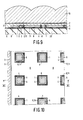
- the infrared detector of Figures 3 and 4 comprises an array of detector elements sandwiched between a substrate 20 and a lens plate 10.
- Each detector element comprises a body 1 of infrared-sensitive semiconductor material having an energy bandgap suitable for detecting infrared radiation up to a specified cut-off wavelength at the operating temperature of the detector.
- the detector elements are normally cooled by thermal conduction through the substrate 20 to a cryogenic cooler.
- the body 1 may be of cadmium mercury telluride whose composition is such that it has a cut-off wavelength of, for example about 12 ⁇ rn at about 77K and about 9tim at about 192K.
- a temperature of about 77K can be obtained with a liquid-nitrogen cryostat (for example a Joule-Thomson cooler, or Stirling engine), whereas a temperature of 192K can be obtained thermoelectrically using a Peltier cooler.
- a liquid-nitrogen cryostat for example a Joule-Thomson cooler, or Stirling engine
- a temperature of 192K can be obtained thermoelectrically using a Peltier cooler.
- each element body 1 is a part of a wider layer 1 and 8 of the infrared-sensitive material which occupies a majority of the volume around the body 1 between the substrate 20 and the lens plate 10. There is present between the layer 1 and 8 and the lens plate 10 an adhesive film 11 by means of which the lens plate 10 is secured over the element bodies 1.
- Each element body 1 is laterally separated around at least a majority of its periphery from the remainder 8 of the layer 1 and 8 by a slot 9.
- the slot 9 extends through the thickness of the layer 1 and 8 (see Figure 4) and defines at least a majority of the periphery of the element body 1 (see Figures 5 and 6).
- the slot 9 extends on three of the four sides of the element body 1 as a U shaped outline around most of the body periphery. In the example of Figure 6, the slot 9 extends on all sides of the element body 1 as a rectangular outline.
- each element body 1 comprises a vertical p-n junction 3 between an n type region 4 at one end of the body 1 and a p type region 2 at the opposite end of the body 1.
- the layer 1 and 8 may be of p type conductivity in which the n type regions may be formed by ion-milling apertures 7 through the thickness of the p type layer by the method disclosed in US-A-4 559 695. Each aperture 7 may then be lined with an electrode 6.
- a thin metal layer (for example of chromium) deposited to form the electrode 6 may also provide the electrode 5 for the p type region 2.
- the structure of the detector elements in this example is such that the slots 9 extend through the entire thickness of the layer 1 and 8.
- the slot 9 may be etched through the layer 1 and 8 using a chemical etchant which does not convert the conductivity type, for example a known etchant solution of bromine in methanol.
- a chemical etchant which does not convert the conductivity type
- a known etchant solution of bromine in methanol for example a known etchant solution of bromine in methanol.
- at least the top and bottom faces of the detector element are passivated, for example with a layer of zinc sulphide. This passivation layer may also extend on the top and bottom faces of the remainder 8 of the layer 1 and 8.
- the substrate 20 may be of, for example, sapphire or another insulating material carrying a metallisation pattern forming conductor tracks as electrical connections for the detector elements (similar to tracks 22 and 24 shown in Figures 1 and 2).
- the layer 1 and 8 is bonded to the substrate 20 by an adhesive film 12, and is processed to form the regions 4, apertures 7, electrodes 5 and 6 and slots 9 in situ on the substrate 20.
- the electrode 6 of each detector element extends in the aperture 7 through the thickness of the body 1 to an underlying part of the substrate connection 24 (which is only shown in Figure 5 where it crosses the slot 9).
- the adhesive film 11 (which may be an insulating epoxy, in a specific example) is present both in the slots 9 and on each element body 1 facing the lens plate 10 so as to bond each detector element to the plate 10.
- the adhesive film between the element body 1 and the lens plate 10 is very thin so that the detector elements are optically immersed on the lens.
- the volume of the adhesive 11 contacting the bodies 1 is greatly reduced in the Figure 4 structure in accordance with the invention, as compared with the Figure 1 structure. This significantly reduces straining of the semiconductor lattice of the cadmium mercury telluride body 1 and its consequent change in the energy bandgap.
- Table 1 illustrates this improvement, in terms of the cut-off wavelength X in ⁇ m measured at two temperatures (77K and 192K) both before and after bonding the lens plate 10 to the detector-element bodies 1 by the adhesive film 11.
- Detector element structures 5a and 5b were those of the specific example of Figures 4 and 5, in which the thickness of the cadmium mercury telluride layer 1 and 8 was about 2.5tim, the element bodies 1 were 10 ⁇ m wide and 15 ⁇ m long, the slots 9 were about sum wide, the width of the layer part 8 between neighbouring element bodies 1 was about 35 ⁇ rn, and the epoxy adhesive film was 100 to 200nm thick on the element bodies 1 and filled the slots 9.
- Detector element structures 2a to 2d were for a comparable specific example of Figures 1 and 2 having the same element body size as for DES 5a and 5b but with the layer part 8 etched away and filled with the epoxy adhesive 11.
- Detector element structures 3a to 3c were for another comparable specific example in which the detector elements 1 of Figures 1 and 2 and of Figures 4 and 5 were replaced with a p type layer of the same thickness as the layer 1 and 8 but having detector elements formed around apertures in the layer as in US-A-4 559 695 and without any slots 9 in the layer.
- the spread in values for the same detector-element structures measured under the same conditions result from the measurement accuracy and slight variations in the thickness of the cadmium mercury telluride and the epoxy adhesive.
- DESs 5a and 5b in accordance with the invention had a higher junction resistance which seems to result from the slots 9 extending on three of the four sides of the element body so restricting the volume of p type material which contributes to the thermally-generated leakage current of the detector element.
- Table 2 lists similar measurements made on further detector element structures in accordance with the specific example of Figures 4 and 5 and with substantially the same dimensions, but constructed from different slices of cadmium mercury telluride of about the same composition.
- the adhesive 11 may be provided in a rectangular frame around the layer 1 and 8 or for example only along the top and bottom of the Figure 5 drawing. It is desirable to press the lens plate 10 tightly against the layer 1 and 8 during the adhesive bonding in order to minimise the air gap between the detector elements 1 and the lens plate 10 so as to preserve good optical immersion.
- the adhesive also flows into the slots 9 and tends to fill these slots, although they may remain partly unfilled due to trapped pockets of air.
- the width of the slots 9 is preferably kept to a minimum consistent with a reliable manufacturing yield. The minimum reliably reproduceable width for the slots 9 depends on the etching process used for their formation. However, typically, the width of the slots 9 may be between two and three times the thickness of the layer 1 and 8, and preferably is less than five times the thickness of the layer 1 and 8.
- the detector elements shown in Figure 5 are arranged in a row as a linear array.
- the remainder 8 of the layer 1 does not comprise infrared detector elements of the array but merely forms a grid (in the shape of a ladder) which occupies a majority of the volume around the detector-element bodies 1 so as to reduce their straining by the adhesive film 11.
- the row of bodies 1 extend laterally as fingers of a comb from an integral part of the remainder 8 of the layer 1 and 8.
- This integral part underlies an extension of the electrode 5 which forms a common electrical connection to the row of element bodies 1.
- the common extended electrode 5 may electrically contact most (or even the whole) of the p type underlying integral part which may therefore form an electrical part of the common electrical connection of the array.
- the extended electrode 5 may be insulated by a passivation layer of ZnS from the p type underlying integral part which may therefore simply constitute a mechanical support for part of the common electrical connection 5.
- the common extended electrode 5 may extend over the edge of the layer part 8 and onto the substrate conductor 22 (not shown in Figure 5).
- each detector element may be confined to an end face of the p type region 2 of each element body 1 and extend directly from that end face to a conductor track 22 on the substrate 20.
- the body structure of each detector element may even be similar to that of the element bodies 1 of Figure 2, except that the remainder 8 of the layer 1 and 8 which provides the element bodies 1 extends as a grid between and around the element bodies 1 from which it is separated by the slots 9.
- Figure 5 illustrates a single row of the element bodies 1 arranged in a linear array.
- the structure of Figure 5 can be adapted to form two such rows of element bodies 1 by providing a mirror image of the Figure 5 structure at the top half of Figure 5.
- the element bodies 1 of one row may be located in line with corresponding element bodies 1 of the other row.
- the element bodies 1 of one row may be located in line with layer parts 8 between neighbouring element bodies 1 of the other row.
- the present invention may also be used for 2-dimensional arrays of detector elements.
- One example of such a 2-dimensional array in accordance with the invention is illustrated in Figure 6, in which the element bodies 1 are isolated parts of the layer 1 and 8, the remainder 8 of which does not comprise any infrared detector elements and forms a rectangular grid network around the element bodies 1 from which it is separated by the slots 9.
- the electrodes 5 to the p type region 2 of each detector element may extend on an end face of the element body 1.
- the electrodes 6 to the n type regions 4 may extend on an opposite end face of each body 1 or in a aperture 7 in each element body 1.
- the grid 8 it is also possible to use the grid 8 to support (or even form an electrical part of) a common connection to the p type regions 2 of the detector elements by having the slot 9 on three sides only (i.e. not at the p type end) of each element body 1.
- an insulating substrate 20 with conductor tracks 24 and 25 may be used (similar to the previous embodiments).
- the substrate 20 may be, for example, a silicon integrated circuit comprising both connections for the detector elements and circuitry for processing the signals from the detector elements.
- the lens plate 10 is bonded by the adhesive film 11 to the layer 1 and 8 which is already mounted on the substrate 20.
- Figure 7 illustrates another embodiment in which the layer 1 and 8 is first provided on the lens plate 10, and the substrate 20 is then bonded by the adhesive film 11 to the layer 1 and 8 on the lens plate 10.
- the layer 1 and 8 may be of crystalline material (for example cadmium mercury telluride) epitaxially grown on the lens plate 10 which may be of for example monocrystalline cadmium telluride or for example monocrystalline silicon coated with cadmium telluride at the face where the cadmium mercury telluride layer 1 and 8 is to be deposited.
- the detector elements may be connected to circuitry formed in parts of the silicon lens plate adjacent to the part 8 of the cadmium mercury telluride layer 1 and 8.
- the invention may also be used with other optical elements.
- the element bodies 1 and the remainder 8 of the layer 1 and 8 may be sandwiched between a substrate 20 and an optical plate 10 comprising an array of prismatic elements corresponding to the array of detector-elements (for example as in GB-A-1 525 562), or even a wedge-shaped plate or single lens element over the whole of an array (for example as in Figures 2,5,8 and 9 of United Kingdom patent application 8531497.9 published as GB-A-2 240 444 on 31st July 1991).
- the whole contents of GB-A-2 240 444 are hereby incorporated herein as reference material.
- the embodiments described so far show only a single level of detector elements between the substrate 20 and the optical element 10, the invention may be applied to each level of a multiple-level detector array structure (for example as described in pending United Kingdom patent application 9022464.3, our reference PHB33674, filed on 17th October 1990 and published as GB-A-2 248 964 on 22nd April 1992).
- the whole contents of GB-A-2 248 964 are hereby incorporated herein as reference material.
- the two levels may comprise different infrared-sensitive semiconductor materials having different bandgaps so as to provide different infrared wavelength responses.
- the lower level may be mounted on, for example, a silicon integrated circuit 20 via an epoxy adhesive layer.
- the upper level of detector elements may have the layer structure 1 and 8 illustrated in Figure 6, whereas the lower level may have the layer structure 1 and 8 illustrated in Figure 8.
- the slots 9 not only separate the lower element bodies 1 from the remainder of the layer 8 but also isolate both n type islands 84 and p type islands 85 from the p type remainder 8 of the layer and from the lower element bodies 1.
- the element bodies 1 are superimposed as a cross centred on the symbol +' in Figures 6 and 7 and the n type region 4 of the upper detector elements overlies a lower n type island 84.
- the aperture 7 through the upper region 4 is continued through the underlying island 84 as an aperture 87 to carry the upper-level electrode 6 to the circuit substrate 20.
- the upper-level electrode 5 may be carried to the circuit substrate 20 via the p type islands 85.
- the upper layer 1 and 8 of Figure 6 is bonded to the lower layer 1 and 8 of Figure 8 by an adhesive film, and an optical element 10 is bonded to the upper layer 1 and 8 of Figure 6 by the film 11 as previously described.
- the slots 9 in the layer 1 and 8 may isolate islands 84 and 85 from the element bodies 1 and the remainder 8 of the layer 1 and 8.
- the detector element connections may comprise the islands 84 and 85 which are electrically connected to the element body 1 by bridging conductor tracks extending over an insulating filling in the slots 9.
- the detector elements in the embodiments of Figures 4 to 8 comprise a vertical p-n junction 3, and the slots 9 extend through the entire thickness of the layer 1 and 8 to define the periphery of each element body 1.
- the embodiment of Figures 9 and 10 illustrates a modified detector-element structure having a horizontal p-n junction 3 between an n type region 4 and an underlying p type region 2.
- the total semiconductor layer 1 and 8 in this example comprises a p type sub-layer 2 adjacent one face and n type regions adjacent its opposite face.
- the slots 9 are present in this opposite face and extend through only a part of the thickness of the layer 1 and 8 to the n type sub-layer 2.
- the total thickness of the layer 1 and 8 may be 10 ⁇ rn whereas the slots 9 may have a depth of 6 ⁇ rn.
- the p type sub-layer 2 provides a common electrical connection of the array of detector elements, and it may extend to the opposite face (for example at a peripheral region of the layer 1 and 8) where an electrode 5 may be provided.
- the n type regions adjacent this opposite face may be restricted to the areas of the element bodies 1, or they may be present also in the remainder 8 of the layer in which case (as shown in Figures 9 and 10) they are isolated from the element regions 4 by the slots 9.
- the element bodies 1 have individual electrodes 6 contacting their regions 4.
- Figure 10 illustrates this embodiment as a modification of the Figure 7 arrangement in which the layer 1 and 8 is of cadmium mercury telluride epitaxially grown on a cadmium telluride buffer layer on the lens plate 10.
- one or more slotted infrared-sensitive semiconductor layers 1 and 8 occupies most of the thickness between the substrate 20 and optical element 10.
- the detector elements may comprise a slotted layer 1 and 8 of such infrared-sensitive semiconductor material (for example cadmium mercury telluride) on a thick insulating layer (for example cadmium telluride), and this thick insulating layer may even occupy as much as half of the thickness between the substrate 20 and the optical element 10.
Landscapes
- Light Receiving Elements (AREA)
- Solid State Image Pick-Up Elements (AREA)
- Transforming Light Signals Into Electric Signals (AREA)
Applications Claiming Priority (2)
| Application Number | Priority Date | Filing Date | Title |
|---|---|---|---|
| GB9116307 | 1991-07-29 | ||
| GB919116307A GB9116307D0 (en) | 1991-07-29 | 1991-07-29 | Infrared detectors |
Publications (2)
| Publication Number | Publication Date |
|---|---|
| EP0525876A1 true EP0525876A1 (fr) | 1993-02-03 |
| EP0525876B1 EP0525876B1 (fr) | 1996-05-08 |
Family
ID=10699140
Family Applications (1)
| Application Number | Title | Priority Date | Filing Date |
|---|---|---|---|
| EP92202222A Expired - Lifetime EP0525876B1 (fr) | 1991-07-29 | 1992-07-20 | Détecteurs infrarouges |
Country Status (4)
| Country | Link |
|---|---|
| US (1) | US5306915A (fr) |
| EP (1) | EP0525876B1 (fr) |
| DE (1) | DE69210497T2 (fr) |
| GB (1) | GB9116307D0 (fr) |
Cited By (14)
| Publication number | Priority date | Publication date | Assignee | Title |
|---|---|---|---|---|
| DE19641272A1 (de) * | 1996-10-07 | 1998-04-09 | Franz Heinz Guenther | Verfahren zum Herstellen von opto-elektronischen Hybrid-Bauteilen mit Blenden |
| DE10222960A1 (de) * | 2002-05-23 | 2003-12-11 | Schott Glas | Verfahren zur Herstellung von elektronischen Bauelementen |
| DE19627543B4 (de) * | 1996-05-18 | 2004-05-06 | Thomas Hofmann | Multi-Layer-Substrat sowie Verfahren zu seiner Herstellung |
| WO2004023564A3 (fr) * | 2002-09-09 | 2005-01-13 | Koninkl Philips Electronics Nv | Dispositif semi-conducteur et procede de fabrication |
| FR2869462A1 (fr) * | 2004-04-21 | 2005-10-28 | Fr De Detecteurs Infrarouges S | Procede pour la realisation d'un detecteur de rayonnement electromagnetique, et notamment infrarouge |
| DE19816309B4 (de) * | 1997-04-14 | 2008-04-03 | CiS Institut für Mikrosensorik gGmbH | Verfahren zur Direktmontage von Silizium-Sensoren und danach hergestellte Sensoren |
| US9635727B2 (en) | 2008-10-24 | 2017-04-25 | Ilumisys, Inc. | Light and light sensor |
| US9777893B2 (en) | 2000-02-11 | 2017-10-03 | Ilumisys, Inc. | Light tube and power supply circuit |
| US9807842B2 (en) | 2012-07-09 | 2017-10-31 | Ilumisys, Inc. | System and method for controlling operation of an LED-based light |
| US10571115B2 (en) | 2008-10-24 | 2020-02-25 | Ilumisys, Inc. | Lighting including integral communication apparatus |
| US10690296B2 (en) | 2015-06-01 | 2020-06-23 | Ilumisys, Inc. | LED-based light with canted outer walls |
| US10713915B2 (en) | 2008-10-24 | 2020-07-14 | Ilumisys, Inc. | Integration of LED lighting control with emergency notification systems |
| CN112057745A (zh) * | 2019-06-11 | 2020-12-11 | 乐金显示有限公司 | 用于皮肤管理或皮肤治疗的电子装置 |
| US10973094B2 (en) | 2008-10-24 | 2021-04-06 | Ilumisys, Inc. | Integration of LED lighting with building controls |
Families Citing this family (39)
| Publication number | Priority date | Publication date | Assignee | Title |
|---|---|---|---|---|
| JP2833450B2 (ja) * | 1993-11-24 | 1998-12-09 | 日本電気株式会社 | 赤外線撮像素子 |
| US5593902A (en) * | 1994-05-23 | 1997-01-14 | Texas Instruments Incorporated | Method of making photodiodes for low dark current operation having geometric enhancement |
| US5828068A (en) * | 1996-04-04 | 1998-10-27 | Raytheon Ti Systems, Inc. | Uncooled mercury cadmium telluride infrared devices with integral optical elements |
| IL128450A (en) * | 1999-02-09 | 2002-05-23 | Elop Electrooptics Ind Ltd | Method of bonding an optical element within an enclosure |
| US20080283121A1 (en) * | 2002-05-07 | 2008-11-20 | Nanoptek Corporation | Bandgap-shifted semiconductor surface and method for making same, and apparatus for using same |
| US7485799B2 (en) * | 2002-05-07 | 2009-02-03 | John Michael Guerra | Stress-induced bandgap-shifted semiconductor photoelectrolytic/photocatalytic/photovoltaic surface and method for making same |
| US7995871B2 (en) * | 2002-05-07 | 2011-08-09 | Nanoptek Corporation | Stress-induced bandgap-shifted semiconductor photoelectrolytic/photocatalytic/photovoltaic surface and method for making same |
| US8673399B2 (en) * | 2002-05-07 | 2014-03-18 | Nanoptek Corporation | Bandgap-shifted semiconductor surface and method for making same, and apparatus for using same |
| JP2003344548A (ja) * | 2002-05-24 | 2003-12-03 | Seiko Instruments Inc | 放射線検出器 |
| US8118447B2 (en) | 2007-12-20 | 2012-02-21 | Altair Engineering, Inc. | LED lighting apparatus with swivel connection |
| US7712918B2 (en) | 2007-12-21 | 2010-05-11 | Altair Engineering , Inc. | Light distribution using a light emitting diode assembly |
| US8360599B2 (en) | 2008-05-23 | 2013-01-29 | Ilumisys, Inc. | Electric shock resistant L.E.D. based light |
| US7976196B2 (en) | 2008-07-09 | 2011-07-12 | Altair Engineering, Inc. | Method of forming LED-based light and resulting LED-based light |
| US7946729B2 (en) | 2008-07-31 | 2011-05-24 | Altair Engineering, Inc. | Fluorescent tube replacement having longitudinally oriented LEDs |
| US8674626B2 (en) | 2008-09-02 | 2014-03-18 | Ilumisys, Inc. | LED lamp failure alerting system |
| US8256924B2 (en) | 2008-09-15 | 2012-09-04 | Ilumisys, Inc. | LED-based light having rapidly oscillating LEDs |
| US8444292B2 (en) | 2008-10-24 | 2013-05-21 | Ilumisys, Inc. | End cap substitute for LED-based tube replacement light |
| US8324817B2 (en) | 2008-10-24 | 2012-12-04 | Ilumisys, Inc. | Light and light sensor |
| US8556452B2 (en) | 2009-01-15 | 2013-10-15 | Ilumisys, Inc. | LED lens |
| US8362710B2 (en) | 2009-01-21 | 2013-01-29 | Ilumisys, Inc. | Direct AC-to-DC converter for passive component minimization and universal operation of LED arrays |
| US8664880B2 (en) | 2009-01-21 | 2014-03-04 | Ilumisys, Inc. | Ballast/line detection circuit for fluorescent replacement lamps |
| US8330381B2 (en) | 2009-05-14 | 2012-12-11 | Ilumisys, Inc. | Electronic circuit for DC conversion of fluorescent lighting ballast |
| US8299695B2 (en) | 2009-06-02 | 2012-10-30 | Ilumisys, Inc. | Screw-in LED bulb comprising a base having outwardly projecting nodes |
| CA2765200A1 (fr) | 2009-06-23 | 2011-01-13 | Altair Engineering, Inc. | Dispositif d'eclairage comprenant des del et un systeme de commande d'alimentation a decoupage |
| US8541958B2 (en) | 2010-03-26 | 2013-09-24 | Ilumisys, Inc. | LED light with thermoelectric generator |
| WO2011119958A1 (fr) | 2010-03-26 | 2011-09-29 | Altair Engineering, Inc. | Lampe à del interne-externe |
| CA2794512A1 (fr) | 2010-03-26 | 2011-09-29 | Ilumisys, Inc. | Tube de lampe a del avec repartition lumineuse laterale double |
| US8454193B2 (en) | 2010-07-08 | 2013-06-04 | Ilumisys, Inc. | Independent modules for LED fluorescent light tube replacement |
| US8596813B2 (en) | 2010-07-12 | 2013-12-03 | Ilumisys, Inc. | Circuit board mount for LED light tube |
| EP2633227B1 (fr) | 2010-10-29 | 2018-08-29 | iLumisys, Inc. | Mécanismes pour réduire le risque d'électrocution pendant l'installation d'un tube fluorescent |
| US8870415B2 (en) | 2010-12-09 | 2014-10-28 | Ilumisys, Inc. | LED fluorescent tube replacement light with reduced shock hazard |
| US9072171B2 (en) | 2011-08-24 | 2015-06-30 | Ilumisys, Inc. | Circuit board mount for LED light |
| WO2013131002A1 (fr) | 2012-03-02 | 2013-09-06 | Ilumisys, Inc. | Embase de connecteur électrique pour lampe à base de del |
| WO2014008463A1 (fr) | 2012-07-06 | 2014-01-09 | Ilumisys, Inc. | Ensemble d'alimentation électrique pour tube lumineux à del |
| US9285084B2 (en) | 2013-03-14 | 2016-03-15 | Ilumisys, Inc. | Diffusers for LED-based lights |
| US9267650B2 (en) | 2013-10-09 | 2016-02-23 | Ilumisys, Inc. | Lens for an LED-based light |
| EP3097748A1 (fr) | 2014-01-22 | 2016-11-30 | iLumisys, Inc. | Lampe à diodes électroluminescentes à adresses |
| US9510400B2 (en) | 2014-05-13 | 2016-11-29 | Ilumisys, Inc. | User input systems for an LED-based light |
| WO2022163378A1 (fr) * | 2021-01-28 | 2022-08-04 | ソニーグループ株式会社 | Réseau de lentilles et dispositif d'affichage stéréoscopique |
Citations (4)
| Publication number | Priority date | Publication date | Assignee | Title |
|---|---|---|---|---|
| US4352948A (en) * | 1979-09-07 | 1982-10-05 | Massachusetts Institute Of Technology | High-intensity solid-state solar-cell device |
| GB2132757A (en) * | 1982-12-22 | 1984-07-11 | Secr Defence | Infra-red detector assembly |
| GB2138209A (en) * | 1983-04-08 | 1984-10-17 | Telecommunications Sa | Photoconducting detector in optical immersion |
| GB2241605A (en) * | 1985-09-11 | 1991-09-04 | Philips Electronic Associated | Infrared photodiodes, arrays and their manufacture |
Family Cites Families (7)
| Publication number | Priority date | Publication date | Assignee | Title |
|---|---|---|---|---|
| GB1525562A (en) * | 1975-08-19 | 1978-09-20 | Hawker Siddeley Aviation Ltd | Multi-element targets sensitive to incident radiation |
| US4559695A (en) * | 1981-03-27 | 1985-12-24 | U.S. Philips Corporation | Method of manufacturing an infrared radiation imaging device |
| GB2095905B (en) * | 1981-03-27 | 1985-01-16 | Philips Electronic Associated | Infra-red radiation imaging devices and methods for their manufacture |
| JPS61182531A (ja) * | 1985-02-08 | 1986-08-15 | Matsushita Electric Ind Co Ltd | 二次元アレイ赤外検出器 |
| GB2240444B (en) * | 1985-12-20 | 1991-10-30 | Philips Electronic Associated | Imaging array devices and staring array imaging systems |
| JPH01320438A (ja) * | 1988-06-22 | 1989-12-26 | Fujitsu Ltd | 赤外線検知装置 |
| GB2248964A (en) * | 1990-10-17 | 1992-04-22 | Philips Electronic Associated | Plural-wavelength infrared detector devices |
-
1991
- 1991-07-29 GB GB919116307A patent/GB9116307D0/en active Pending
-
1992
- 1992-07-20 EP EP92202222A patent/EP0525876B1/fr not_active Expired - Lifetime
- 1992-07-20 DE DE69210497T patent/DE69210497T2/de not_active Expired - Fee Related
- 1992-07-28 US US07/922,117 patent/US5306915A/en not_active Expired - Fee Related
Patent Citations (4)
| Publication number | Priority date | Publication date | Assignee | Title |
|---|---|---|---|---|
| US4352948A (en) * | 1979-09-07 | 1982-10-05 | Massachusetts Institute Of Technology | High-intensity solid-state solar-cell device |
| GB2132757A (en) * | 1982-12-22 | 1984-07-11 | Secr Defence | Infra-red detector assembly |
| GB2138209A (en) * | 1983-04-08 | 1984-10-17 | Telecommunications Sa | Photoconducting detector in optical immersion |
| GB2241605A (en) * | 1985-09-11 | 1991-09-04 | Philips Electronic Associated | Infrared photodiodes, arrays and their manufacture |
Cited By (27)
| Publication number | Priority date | Publication date | Assignee | Title |
|---|---|---|---|---|
| DE19627543B4 (de) * | 1996-05-18 | 2004-05-06 | Thomas Hofmann | Multi-Layer-Substrat sowie Verfahren zu seiner Herstellung |
| DE19627543B9 (de) * | 1996-05-18 | 2004-10-14 | Thomas Hofmann | Multi-Layer-Substrat sowie Verfahren zu seiner Herstellung |
| DE19641272A1 (de) * | 1996-10-07 | 1998-04-09 | Franz Heinz Guenther | Verfahren zum Herstellen von opto-elektronischen Hybrid-Bauteilen mit Blenden |
| DE19641272C2 (de) * | 1996-10-07 | 2003-03-27 | Franz Heinz Guenther | Verfahren zum Herstellen von opto-elektronischen Hybrid-Bauteilen mit Blenden |
| DE19816309B4 (de) * | 1997-04-14 | 2008-04-03 | CiS Institut für Mikrosensorik gGmbH | Verfahren zur Direktmontage von Silizium-Sensoren und danach hergestellte Sensoren |
| US10557593B2 (en) | 2000-02-11 | 2020-02-11 | Ilumisys, Inc. | Light tube and power supply circuit |
| US9777893B2 (en) | 2000-02-11 | 2017-10-03 | Ilumisys, Inc. | Light tube and power supply circuit |
| DE10222960A1 (de) * | 2002-05-23 | 2003-12-11 | Schott Glas | Verfahren zur Herstellung von elektronischen Bauelementen |
| WO2004023564A3 (fr) * | 2002-09-09 | 2005-01-13 | Koninkl Philips Electronics Nv | Dispositif semi-conducteur et procede de fabrication |
| US7351951B2 (en) | 2002-09-09 | 2008-04-01 | Koninklijke Philips Electronics N.V. | Optoelectronic semiconductor device and method of manufacturing such a device |
| CN100550430C (zh) * | 2002-09-09 | 2009-10-14 | 皇家飞利浦电子股份有限公司 | 半导体器件及其制造方法 |
| FR2869462A1 (fr) * | 2004-04-21 | 2005-10-28 | Fr De Detecteurs Infrarouges S | Procede pour la realisation d'un detecteur de rayonnement electromagnetique, et notamment infrarouge |
| US9635727B2 (en) | 2008-10-24 | 2017-04-25 | Ilumisys, Inc. | Light and light sensor |
| US10560992B2 (en) | 2008-10-24 | 2020-02-11 | Ilumisys, Inc. | Light and light sensor |
| US10973094B2 (en) | 2008-10-24 | 2021-04-06 | Ilumisys, Inc. | Integration of LED lighting with building controls |
| US10571115B2 (en) | 2008-10-24 | 2020-02-25 | Ilumisys, Inc. | Lighting including integral communication apparatus |
| US11333308B2 (en) | 2008-10-24 | 2022-05-17 | Ilumisys, Inc. | Light and light sensor |
| US10713915B2 (en) | 2008-10-24 | 2020-07-14 | Ilumisys, Inc. | Integration of LED lighting control with emergency notification systems |
| US11073275B2 (en) | 2008-10-24 | 2021-07-27 | Ilumisys, Inc. | Lighting including integral communication apparatus |
| US10932339B2 (en) | 2008-10-24 | 2021-02-23 | Ilumisys, Inc. | Light and light sensor |
| US9807842B2 (en) | 2012-07-09 | 2017-10-31 | Ilumisys, Inc. | System and method for controlling operation of an LED-based light |
| US10966295B2 (en) | 2012-07-09 | 2021-03-30 | Ilumisys, Inc. | System and method for controlling operation of an LED-based light |
| US11028972B2 (en) | 2015-06-01 | 2021-06-08 | Ilumisys, Inc. | LED-based light with canted outer walls |
| US10690296B2 (en) | 2015-06-01 | 2020-06-23 | Ilumisys, Inc. | LED-based light with canted outer walls |
| US11428370B2 (en) | 2015-06-01 | 2022-08-30 | Ilumisys, Inc. | LED-based light with canted outer walls |
| CN112057745A (zh) * | 2019-06-11 | 2020-12-11 | 乐金显示有限公司 | 用于皮肤管理或皮肤治疗的电子装置 |
| CN112057745B (zh) * | 2019-06-11 | 2023-06-23 | 乐金显示有限公司 | 用于皮肤管理或皮肤治疗的电子装置 |
Also Published As
| Publication number | Publication date |
|---|---|
| EP0525876B1 (fr) | 1996-05-08 |
| DE69210497D1 (de) | 1996-06-13 |
| GB9116307D0 (en) | 1991-11-06 |
| DE69210497T2 (de) | 1996-09-05 |
| US5306915A (en) | 1994-04-26 |
Similar Documents
| Publication | Publication Date | Title |
|---|---|---|
| EP0525876B1 (fr) | Détecteurs infrarouges | |
| US5185648A (en) | Plural-wavelength infrared detector devices | |
| US6111254A (en) | Infrared radiation detector | |
| US6355939B1 (en) | Multi-band infrared photodetector | |
| CA2220834C (fr) | Photodetecteur ir a puits quantiques ameliore | |
| US4783594A (en) | Reticular detector array | |
| EP0481552B1 (fr) | Dispositifs de detecteurs infrarouges | |
| EP0864171B1 (fr) | Formation de contacts sur des substrats semi-conducteurs destines a des detecteurs de rayonnement et a des dispositifs d'imagerie | |
| US4972244A (en) | Photodiode and photodiode array on a II-VI material and processes for the production thereof | |
| EP0087842B1 (fr) | Détecteurs de rayonnement infrarouge et leur fabrication | |
| US5264699A (en) | Infrared detector hybrid array with improved thermal cycle reliability and method for making same | |
| KR100274124B1 (ko) | 전기 광 검출기 어레이 | |
| US5401986A (en) | Bake-stable HgCdTe photodetector with II-VI passivation layer | |
| US5751049A (en) | Two-color infrared detector | |
| US5296384A (en) | Bake-stable HgCdTe photodetector and method for fabricating same | |
| US6198100B1 (en) | Method for fabricating an infrared radiation detector | |
| US5517029A (en) | Dual-band IR scanning focal plane assembly having two monolithically integrated linear detector arrays for simultaneous image readout | |
| GB2241605A (en) | Infrared photodiodes, arrays and their manufacture | |
| US4801802A (en) | Imaging, device, elements and systems | |
| CA1088190A (fr) | Conversion photo-electrique integree | |
| GB2239555A (en) | Infrared image-sensing devices and their manufacture | |
| JP2705594B2 (ja) | 赤外線検出素子 | |
| EP0248881A1 (fr) | Structure et procede de fabrication d'un photodetecteur a mode de piegeage | |
| HK1010282B (en) | Forming contacts on semiconductor substrates for radiation detectors and imaging devices | |
| IL106458A (en) | Bake-stable HgCdTe photodetector and method for fabricating same |
Legal Events
| Date | Code | Title | Description |
|---|---|---|---|
| PUAI | Public reference made under article 153(3) epc to a published international application that has entered the european phase |
Free format text: ORIGINAL CODE: 0009012 |
|
| AK | Designated contracting states |
Kind code of ref document: A1 Designated state(s): DE FR GB |
|
| 17P | Request for examination filed |
Effective date: 19930713 |
|
| R17P | Request for examination filed (corrected) |
Effective date: 19930719 |
|
| RAP1 | Party data changed (applicant data changed or rights of an application transferred) |
Owner name: GEC-MARCONI LIMITED |
|
| 17Q | First examination report despatched |
Effective date: 19950727 |
|
| GRAH | Despatch of communication of intention to grant a patent |
Free format text: ORIGINAL CODE: EPIDOS IGRA |
|
| GRAA | (expected) grant |
Free format text: ORIGINAL CODE: 0009210 |
|
| AK | Designated contracting states |
Kind code of ref document: B1 Designated state(s): DE FR GB |
|
| REF | Corresponds to: |
Ref document number: 69210497 Country of ref document: DE Date of ref document: 19960613 |
|
| ET | Fr: translation filed | ||
| PLBE | No opposition filed within time limit |
Free format text: ORIGINAL CODE: 0009261 |
|
| 26N | No opposition filed | ||
| PGFP | Annual fee paid to national office [announced via postgrant information from national office to epo] |
Ref country code: FR Payment date: 19980611 Year of fee payment: 7 |
|
| PGFP | Annual fee paid to national office [announced via postgrant information from national office to epo] |
Ref country code: GB Payment date: 19980626 Year of fee payment: 7 |
|
| PGFP | Annual fee paid to national office [announced via postgrant information from national office to epo] |
Ref country code: DE Payment date: 19980629 Year of fee payment: 7 |
|
| PG25 | Lapsed in a contracting state [announced via postgrant information from national office to epo] |
Ref country code: GB Free format text: LAPSE BECAUSE OF NON-PAYMENT OF DUE FEES Effective date: 19990720 |
|
| PG25 | Lapsed in a contracting state [announced via postgrant information from national office to epo] |
Ref country code: FR Free format text: THE PATENT HAS BEEN ANNULLED BY A DECISION OF A NATIONAL AUTHORITY Effective date: 19990731 |
|
| GBPC | Gb: european patent ceased through non-payment of renewal fee |
Effective date: 19990720 |
|
| PG25 | Lapsed in a contracting state [announced via postgrant information from national office to epo] |
Ref country code: DE Free format text: LAPSE BECAUSE OF NON-PAYMENT OF DUE FEES Effective date: 20000503 |
|
| REG | Reference to a national code |
Ref country code: FR Ref legal event code: ST |