EP0864171B1 - Formation de contacts sur des substrats semi-conducteurs destines a des detecteurs de rayonnement et a des dispositifs d'imagerie - Google Patents
Formation de contacts sur des substrats semi-conducteurs destines a des detecteurs de rayonnement et a des dispositifs d'imagerie Download PDFInfo
- Publication number
- EP0864171B1 EP0864171B1 EP96941641A EP96941641A EP0864171B1 EP 0864171 B1 EP0864171 B1 EP 0864171B1 EP 96941641 A EP96941641 A EP 96941641A EP 96941641 A EP96941641 A EP 96941641A EP 0864171 B1 EP0864171 B1 EP 0864171B1
- Authority
- EP
- European Patent Office
- Prior art keywords
- contacts
- layer
- substrate
- metal
- radiation detector
- Prior art date
- Legal status (The legal status is an assumption and is not a legal conclusion. Google has not performed a legal analysis and makes no representation as to the accuracy of the status listed.)
- Expired - Lifetime
Links
- 239000000758 substrate Substances 0.000 title claims abstract description 70
- 230000005855 radiation Effects 0.000 title claims abstract description 46
- 239000004065 semiconductor Substances 0.000 title claims abstract description 34
- 238000003384 imaging method Methods 0.000 title claims description 19
- 239000000463 material Substances 0.000 claims abstract description 66
- 229910052751 metal Inorganic materials 0.000 claims abstract description 62
- 239000002184 metal Substances 0.000 claims abstract description 62
- 238000000034 method Methods 0.000 claims abstract description 53
- PCHJSUWPFVWCPO-UHFFFAOYSA-N gold Chemical compound [Au] PCHJSUWPFVWCPO-UHFFFAOYSA-N 0.000 claims abstract description 37
- 239000010931 gold Substances 0.000 claims abstract description 36
- 229910052737 gold Inorganic materials 0.000 claims abstract description 34
- 238000002161 passivation Methods 0.000 claims abstract description 29
- QWUZMTJBRUASOW-UHFFFAOYSA-N cadmium tellanylidenezinc Chemical compound [Zn].[Cd].[Te] QWUZMTJBRUASOW-UHFFFAOYSA-N 0.000 claims description 40
- BASFCYQUMIYNBI-UHFFFAOYSA-N platinum Chemical compound [Pt] BASFCYQUMIYNBI-UHFFFAOYSA-N 0.000 claims description 16
- 239000004020 conductor Substances 0.000 claims description 12
- PIGFYZPCRLYGLF-UHFFFAOYSA-N Aluminum nitride Chemical compound [Al]#N PIGFYZPCRLYGLF-UHFFFAOYSA-N 0.000 claims description 10
- 238000004519 manufacturing process Methods 0.000 claims description 10
- 229910017083 AlN Inorganic materials 0.000 claims description 9
- MARUHZGHZWCEQU-UHFFFAOYSA-N 5-phenyl-2h-tetrazole Chemical compound C1=CC=CC=C1C1=NNN=N1 MARUHZGHZWCEQU-UHFFFAOYSA-N 0.000 claims description 8
- 229910052697 platinum Inorganic materials 0.000 claims description 7
- 229910052738 indium Inorganic materials 0.000 claims description 5
- APFVFJFRJDLVQX-UHFFFAOYSA-N indium atom Chemical compound [In] APFVFJFRJDLVQX-UHFFFAOYSA-N 0.000 claims description 5
- 230000005250 beta ray Effects 0.000 claims description 4
- 230000005251 gamma ray Effects 0.000 claims description 4
- 238000004544 sputter deposition Methods 0.000 claims description 4
- 238000000151 deposition Methods 0.000 claims description 3
- 230000008021 deposition Effects 0.000 claims description 2
- 230000008020 evaporation Effects 0.000 claims description 2
- 238000001704 evaporation Methods 0.000 claims description 2
- 229910004611 CdZnTe Inorganic materials 0.000 abstract 1
- 230000015556 catabolic process Effects 0.000 abstract 1
- 238000006731 degradation reaction Methods 0.000 abstract 1
- 239000010410 layer Substances 0.000 description 39
- 229920002120 photoresistant polymer Polymers 0.000 description 13
- 238000000926 separation method Methods 0.000 description 5
- 230000010354 integration Effects 0.000 description 4
- 238000009825 accumulation Methods 0.000 description 3
- PMHQVHHXPFUNSP-UHFFFAOYSA-M copper(1+);methylsulfanylmethane;bromide Chemical compound Br[Cu].CSC PMHQVHHXPFUNSP-UHFFFAOYSA-M 0.000 description 3
- 230000003647 oxidation Effects 0.000 description 3
- 238000007254 oxidation reaction Methods 0.000 description 3
- VYPSYNLAJGMNEJ-UHFFFAOYSA-N Silicium dioxide Chemical compound O=[Si]=O VYPSYNLAJGMNEJ-UHFFFAOYSA-N 0.000 description 2
- XUIMIQQOPSSXEZ-UHFFFAOYSA-N Silicon Chemical compound [Si] XUIMIQQOPSSXEZ-UHFFFAOYSA-N 0.000 description 2
- 238000004026 adhesive bonding Methods 0.000 description 2
- 239000012790 adhesive layer Substances 0.000 description 2
- 229910052782 aluminium Inorganic materials 0.000 description 2
- 239000004411 aluminium Substances 0.000 description 2
- XAGFODPZIPBFFR-UHFFFAOYSA-N aluminium Chemical compound [Al] XAGFODPZIPBFFR-UHFFFAOYSA-N 0.000 description 2
- 229920001940 conductive polymer Polymers 0.000 description 2
- 238000007796 conventional method Methods 0.000 description 2
- 230000000694 effects Effects 0.000 description 2
- 230000002708 enhancing effect Effects 0.000 description 2
- 150000002739 metals Chemical class 0.000 description 2
- 239000002861 polymer material Substances 0.000 description 2
- 229910052710 silicon Inorganic materials 0.000 description 2
- 239000010703 silicon Substances 0.000 description 2
- 229910052814 silicon oxide Inorganic materials 0.000 description 2
- 238000010521 absorption reaction Methods 0.000 description 1
- 238000007792 addition Methods 0.000 description 1
- 230000002411 adverse Effects 0.000 description 1
- 229910045601 alloy Inorganic materials 0.000 description 1
- 239000000956 alloy Substances 0.000 description 1
- 230000015572 biosynthetic process Effects 0.000 description 1
- 230000001419 dependent effect Effects 0.000 description 1
- 230000006866 deterioration Effects 0.000 description 1
- 230000007613 environmental effect Effects 0.000 description 1
- 238000005530 etching Methods 0.000 description 1
- 238000001465 metallisation Methods 0.000 description 1
- 238000012986 modification Methods 0.000 description 1
- 230000004048 modification Effects 0.000 description 1
- 230000003287 optical effect Effects 0.000 description 1
- 238000000206 photolithography Methods 0.000 description 1
- 230000035945 sensitivity Effects 0.000 description 1
Images


Classifications
-
- H—ELECTRICITY
- H10—SEMICONDUCTOR DEVICES; ELECTRIC SOLID-STATE DEVICES NOT OTHERWISE PROVIDED FOR
- H10F—INORGANIC SEMICONDUCTOR DEVICES SENSITIVE TO INFRARED RADIATION, LIGHT, ELECTROMAGNETIC RADIATION OF SHORTER WAVELENGTH OR CORPUSCULAR RADIATION
- H10F77/00—Constructional details of devices covered by this subclass
- H10F77/20—Electrodes
- H10F77/206—Electrodes for devices having potential barriers
-
- H—ELECTRICITY
- H10—SEMICONDUCTOR DEVICES; ELECTRIC SOLID-STATE DEVICES NOT OTHERWISE PROVIDED FOR
- H10D—INORGANIC ELECTRIC SEMICONDUCTOR DEVICES
- H10D84/00—Integrated devices formed in or on semiconductor substrates that comprise only semiconducting layers, e.g. on Si wafers or on GaAs-on-Si wafers
- H10D84/01—Manufacture or treatment
- H10D84/0198—Integrating together multiple components covered by H10D44/00, e.g. integrating charge coupled devices
-
- H—ELECTRICITY
- H10—SEMICONDUCTOR DEVICES; ELECTRIC SOLID-STATE DEVICES NOT OTHERWISE PROVIDED FOR
- H10D—INORGANIC ELECTRIC SEMICONDUCTOR DEVICES
- H10D84/00—Integrated devices formed in or on semiconductor substrates that comprise only semiconducting layers, e.g. on Si wafers or on GaAs-on-Si wafers
- H10D84/01—Manufacture or treatment
- H10D84/02—Manufacture or treatment characterised by using material-based technologies
- H10D84/03—Manufacture or treatment characterised by using material-based technologies using Group IV technology, e.g. silicon technology or silicon-carbide [SiC] technology
- H10D84/038—Manufacture or treatment characterised by using material-based technologies using Group IV technology, e.g. silicon technology or silicon-carbide [SiC] technology using silicon technology, e.g. SiGe
-
- H—ELECTRICITY
- H10—SEMICONDUCTOR DEVICES; ELECTRIC SOLID-STATE DEVICES NOT OTHERWISE PROVIDED FOR
- H10F—INORGANIC SEMICONDUCTOR DEVICES SENSITIVE TO INFRARED RADIATION, LIGHT, ELECTROMAGNETIC RADIATION OF SHORTER WAVELENGTH OR CORPUSCULAR RADIATION
- H10F39/00—Integrated devices, or assemblies of multiple devices, comprising at least one element covered by group H10F30/00, e.g. radiation detectors comprising photodiode arrays
- H10F39/10—Integrated devices
- H10F39/12—Image sensors
- H10F39/18—Complementary metal-oxide-semiconductor [CMOS] image sensors; Photodiode array image sensors
-
- Y—GENERAL TAGGING OF NEW TECHNOLOGICAL DEVELOPMENTS; GENERAL TAGGING OF CROSS-SECTIONAL TECHNOLOGIES SPANNING OVER SEVERAL SECTIONS OF THE IPC; TECHNICAL SUBJECTS COVERED BY FORMER USPC CROSS-REFERENCE ART COLLECTIONS [XRACs] AND DIGESTS
- Y10—TECHNICAL SUBJECTS COVERED BY FORMER USPC
- Y10S—TECHNICAL SUBJECTS COVERED BY FORMER USPC CROSS-REFERENCE ART COLLECTIONS [XRACs] AND DIGESTS
- Y10S438/00—Semiconductor device manufacturing: process
- Y10S438/93—Ternary or quaternary semiconductor comprised of elements from three different groups, e.g. I-III-V
-
- Y—GENERAL TAGGING OF NEW TECHNOLOGICAL DEVELOPMENTS; GENERAL TAGGING OF CROSS-SECTIONAL TECHNOLOGIES SPANNING OVER SEVERAL SECTIONS OF THE IPC; TECHNICAL SUBJECTS COVERED BY FORMER USPC CROSS-REFERENCE ART COLLECTIONS [XRACs] AND DIGESTS
- Y10—TECHNICAL SUBJECTS COVERED BY FORMER USPC
- Y10S—TECHNICAL SUBJECTS COVERED BY FORMER USPC CROSS-REFERENCE ART COLLECTIONS [XRACs] AND DIGESTS
- Y10S438/00—Semiconductor device manufacturing: process
- Y10S438/958—Passivation layer
Definitions
- the invention relates to methods of manufacturing radiation detectors and radiation imaging devices, radiation detectors and imaging devices manufactured by these methods and the use of such imaging devices.
- a typical method of manufacturing a radiation detector for an imaging device comprises applying a layer of a metal such as aluminium to both of the main surfaces of a planar semiconductor substrate, applying a layer of photoresistive material to cover the semiconductor material, exposing the photoresistive material on the surface of the planar substrate with an appropriate mask pattern, removing the photoresistive material to expose a pattern of the metal to be removed, etching away the metal to be removed and then removing the remaining photoresistive material to leave a pattern of contacts on one surface of the substrate and a metallised layer on the other surface of the substrate.
- the contacts on the first surface of the substrate then define an arrangement of radiation detector cells.
- silicon has typically been used for the semiconductor material for the substrate.
- a method of the type described above has been used to good effect with this material.
- CdZnTe cadmium zinc telluride
- X-ray, gamma-ray and to a lesser extent beta-ray, radiation imaging CdZnTe is good at absorbing X-rays and gamma-rays giving better than 90% efficiency for 100keV X-rays and gamma-rays with a 2mm thick detector.
- the leakage or dark current of these detectors can be controlled and values of the order of 10nA/cm 2 or less at 100Volts bias are achievable.
- a readout chip then can be 'flip-chip' joined to the patterned side of the CdZnTe detector (e.g., by bump bonding using balls of indium or conductive polymer material, gluing using one-way conductive materials or other conductive adhesive layer techniques) so that the position dependent electrical signals which result from incidence and absorption in the detector cells of X-rays or gamma-rays can be processed.
- the readout chip could be of the pulse counting type with very fast integration and processing time (typical a few microseconds or at most a few milliseconds). Alternatively, it may be one of the type which provides for charge accumulation for individual detector cells. With an imaging device of this type, integration times can be several milliseconds, or tens or hundreds of milliseconds. As the signal integration or standby/readout period increases it becomes more critical that the gold or platinum contacts on the CdZnTe surface are electrically separated to a high degree to avoid signals from neighbouring contacts (pixel pads) leaking and causing the contrast resolution to
- a method of manufacturing a radiation detector having a plurality of detector cell contacts on a first surface of a semiconductor radiation detector substrate at positions for defining radiation detector cells and a layer of conductive material on a second surface of said substrate opposite to said first surface, said substrate being formed from cadmium zinc telluride or cadmium telluride semiconductor material for detecting x-rays, gamma-rays or beta-rays, and said cell contacts and said layer of conductive material being on said first and second surfaces, respectively of said semiconductor material, wherein said method includes steps of forming said contacts on said first surface including steps of:
- the present inventors have found that the surface resistivity of a CdTe or a CdZnTe semiconductor substrate is degraded when the substrate is exposed to metal etchants suitable for removing gold and/or platinum. As a result of this, the electrical separation of the individual contacts which result from the conventional method of forming such contacts is not as good as would be expected from the properties of that material before treatment.
- the surface of the semiconductor substrate between the contacts can be isolated from the metal etchants, thus preventing the damage which would result if the metal etchants came into contact with the semiconductor surface.
- an insulating layer of passivation material means that after manufacture of the detector, the passivation material remains between the contacts protecting the semiconductor surface from environmental damage in use and further enhancing the electrical separation of the contacts.
- step (a) comprises a further substep: a(vii) removing remaining photoresistive material of said photoresistive material layer.
- photoresistive material an additionally be applied to all exposed surfaces prior to step a(v).
- the areas corresponding generally to the openings are larger than the corresponding openings, so that after the removal in step c(iii) of the metal not covered by the photoresistive material of the further layer, the contacts cover the opening and also extend up and laterally beyond the opening. In this way the ingress of metal etchant around the photoresistive material, whereby the metal etchant might reach the semiconductor surface, can be avoided.
- the invention finds particular use with substrates formed of cadmium zinc telluride (CdZnTe).
- the metal layer for forming the contacts is applied by a method such as sputtering, evaporation or electrolytic deposition, preferably by sputtering.
- the metal layer for forming the contacts comprises gold (Au), although other metals, for example platinum (Pt) or indium (In), could also be used.
- Au gold
- other metals for example platinum (Pt) or indium (In), could also be used.
- Step (c) can comprise removing unwanted metal by a photoresist liftoff technique, although more typically step (c) comprises removing unwanted metal by means of an appropriate metal etchant.
- Each metal contact can define a respective pixel cell of an array of pixel cells, or one of a plurality of strips arranged parallel to each other, depending on the application of the detector.
- the metal contacts can be of the order of 10 ⁇ m across with a spacing of the order of 5 ⁇ m.
- the invention further provides a method of manufacturing a radiation imaging device comprising:
- a radiation detector comprising a semiconductor substrate for detecting radiation with a plurality of metal contacts for respective radiation detector cells on a first surface thereof and with a layer of conductive material on a second surface of said substrate opposite to said first surface, wherein said substrate is formed from cadmium zinc telluride or cadmium telluride semiconductor material for detecting x-rays, gamma-rays or beta-rays, and said cell contacts and said layer or conductive material are on said first and second surfaces, respectively of said semiconductor material, the overall width of a said metal contact is larger than the width of said contact adjacent said substrate, and aluminium nitride passivation material extends between individual contacts and said first surface of said substrate.
- the semiconductor substrate is made of cadmium zinc telluride (CdZnTe).
- CeZnTe cadmium zinc telluride
- Aluminium nitride has been found to be particularly effective as a passivation material for CdZnTe because it can be applied at low temperature, CdZnTe being temperature sensitive.
- the metal contacts can define an array of pixel cells, or a plurality of strips arranged parallel to each other, depending on the field of use of the detector.
- Pixel contacts formed on detector substrate are preferably substantially circular and are arranged in a plurality of rows, more preferably with alternate rows preferably being offset from adjacent rows.
- the metal contacts are of the order of 10 ⁇ m across with a spacing of the order of 5 ⁇ m.
- the resistivity between metal contacts should be in excess of 1G ⁇ /square, preferably in excess of 10G ⁇ /square, more preferably in excess of 100G ⁇ /square and even more preferably in excess of 1000G ⁇ /square (1 T ⁇ /square).
- a radiation imaging device in accordance with the invention finds particular application for X-ray, gamma-ray and beta-ray imaging.
- an embodiment of the invention can provide a method for manufacturing, for example, detectors having a CdZnTe substrate with one side uniformly metallised with gold and the other side patterned with gold structures in a manner that does not adversely affect the surface characteristics of the CdZnTe substrate between the gold structures.
- a method can be provided for creating gold structures on one side of a CdZnTe detector, the method achieving inter-structure resistivity of the order of G ⁇ /square or tens or hundreds of G ⁇ /square.
- an electrically insulating passivation layer between contacts further enables the area between metal contacts to be protected, thus giving the detector stable performance over time and avoiding effects such as oxidation which increase the surface leakage current and decrease the inter-contact resistivity.
- Aluminum nitride (AlN) passivation has been found to be particularly effective when applied between gold contacts to protect the surface and enhance the electrical separation of the gold contacts.
- the passivation layer of aluminium nitride can be implemented at relatively low temperatures typically less than 100°C.
- silicon oxide (SiO 2 ) which is typically used as a passivant for silicon (Si) semiconductors, needs temperatures in excess of 200°C. After exposure to these temperatures, CdZnTe would be unusable.
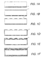
- Figure 1 illustrates a method of forming metal contacts on a semiconductor substrate at positions for defining radiation detector cells.
- the semiconductor substrate is made of cadmium zinc telluride (CdZnTe), although it will be appreciated that cadmium telluride (CdTe) can be used.
- the metal used for the metallisation layer and the gold contacts is gold, although it will be appreciated that other metals, alloys or other conductive materials, for example platinum or indium, could be used.
- Figure 1 is a schematic cross-sectional view from the side of a detector substrate at various stages in the formation of gold contacts on a CdZnTe substrate.
- the end result is a CdZnTe detector with the lower face 2 uniformly metallised with gold and the upper face metallized with gold 9 in a desired pattern.
- the method ensures that at no stage the gold etchant comes in contact with the CdZnTe surface.
- the area 10 between the final gold patterns (pixel pads) 9 thus remains totally unharmed and is not influenced by the gold etchant.
- the surface of the CdZnTe retains very high resistivity, in excess of IG ⁇ /square between gold pixel pads 9, and very low surface leakage current.
- the inter-pixel resistivity can be tens, hundreds or even few thousands of G ⁇ /square without compromising pixel resolution. Indeed 300G ⁇ /square has been measured and values in excess of a TO/square are achievable.
- a passivation layer can be applied between the gold pixel pads. Passivation will ensure a stable performance over time, by avoiding oxidation of the surface not covered by gold. Passivation also enhances the inter-pixel resistivity.
- One problem is the compatibility of the passivation layer with respect to CdZnTe. The inventors have found that aluminum nitride is an appropriate passivation material for CdZnTe.
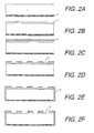
- Figure 2 illustrates a method in accordance with the invention of forming metal contacts on a semiconductor substrate at positions for defining radiation detector cells with a layer of passivation material between the metal contacts.
- the passivation material is aluminium nitride.
- the gold etchant or indeed the aluminium nitride etchant come in contact with the regions 20 between the gold pixel contacts 21 or the edges and sides of the CdZnTe detector.
- the surface of the substrate at 20 between the gold contacts 21 remains unharmed, retaining very high resistivity of the order of GO/square, tens, hundreds or even thousands of G ⁇ /square.
- the aluminum nitride passivation covers the area 20 between the metal contacts 21 protecting the corresponding regions form oxidation (providing stability over time) and enhancing the inter-contact resistivity.
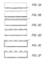
- a result of the method of Figure 3 is that the resultant pixel pads are flatter (i.e. they have a lower profile) than with the method of Figure 2, as can be seen by comparing Figures 2K and 3L.
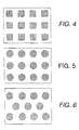
- Figures 4, 5 and 6 are used to illustrate possible pixel contact patterns on the upper surface of the detector substrate.
- an array of square pixel contact pads is shown.
- an array of circular pixel pads is shown.
- the use of circular rather than square pixel pads increases the surface resistance between pads by increasing the amount of resistive material between adjacent pads.
- Figure 6 illustrates an array of offset (honeycombed) pixel pads. Once again this further increases the resistance between pads by increasing the surface amount of resistive material between adjacent pads.
- gold is an advantageous material because it can be readily etched to define the desired contact structures and give good contact (better than aluminium, for example) to the CdZnTe, it is apparent that the procedure disclosed above could also be applied for any kind of metal contacts (e.g. platinum) in combination with an appropriate etchant.
- metal contacts e.g. platinum
- the longitudinal dimensions (width) of the top of the gold contacts 9 (Figure 1), 21 ( Figure 2) or 32 ( Figure 3) is larger than that at the gold-substrate interface. This arises from the relative sizes of the openings to the substrate surface and the photoresist left over the portions for forming the contacts to ensure that, when redundant gold is etched away, the etchant will not seep through to the interface between first layer of photoresist (or the passivation layer) and gold in the openings.
- a radiation imaging device can be constructed by connecting a radiation detector produced by the method according to one of the above described methods to a readout chip having circuits for accumulating charge from successive radiation hits, individual contacts (e.g. pixel pads) for respective detector cells being 'flip-chip' joined (e.g., by bump bonding using balls of indium or conductive polymer material, gluing using one-way conductive materials, or other conductive adhesive layer techniques) to respective circuits for accumulating charge.
- the invention teaches how to obtain a radiation detector (e.g. based on a CdZnTe substrate) with one side metallised according to a desired pattern with maximum possible electrical resistivity separation between the metal contacts.
- a radiation detector e.g. based on a CdZnTe substrate
- High resistivity between metal contacts is desirable to improve contrast resolution and eliminate signal leakage between adjacent metal contacts on the substrate surface. This is particularly relevant when long charge accumulation times and long standby/readout times are employed by the readout chip.
- Such accumulation and standby/readout times could, for example, be in excess of 1msec in examples of imaging devices using a radiation detector manufactured in accordance with the present invention.
- imaging devices find application, for example, for X-ray, gamma-ray and beta-ray imaging.
Landscapes
- Light Receiving Elements (AREA)
- Solid State Image Pick-Up Elements (AREA)
- Measurement Of Radiation (AREA)
- Apparatus For Radiation Diagnosis (AREA)
- Electrodes Of Semiconductors (AREA)
Claims (22)
- Procédé de fabrication d'un détecteur de radiations comportant une pluralité de contacts de cellule de détecteur (21) sur une première surface d'un substrat de détecteur de radiations à semiconducteurs (1) en des positions permettant de définir des cellules de détecteur de radiations et une couche (2) de matériau conducteur sur une deuxième surface dudit substrat opposée à ladite première surface, ledit substrat étant formé en matériau semiconducteur en tellurure de cadmium et de zinc ou en tellurure de cadmium pour détecter des rayons X, des rayons gamma ou des rayons bêta, et lesdits contacts de cellule et ladite couche de matériau conducteur se trouvant sur lesdites première et deuxième surfaces, respectivement, dudit matériau semiconducteur, ledit procédé comprenant des étapes de formation desdits contacts sur ladite première surface, comprenant les étapes suivantes :a) la formation de couches sur ladite première surface dudit substrat avec des ouvertures vers ladite surface de substrat auxdites positions de contact, comprenant les sous-étapes suivantes :a(i) la formation d'une couche (11) de matériau de passivation en nitrure d'aluminium sur ladite première surface de substrat ;a(ii) la formation d'une couche de matériau de photoréserve (12) sur ladite couche de passivation ;a(iii) l'exposition sélective dudit matériau de photoréserve ;a(iv) le retrait dudit matériau de photoréserve des zones correspondant auxdites positions de contact afin d'exposer ladite couche de matériau de passivation (11) ;a(v) le retrait dudit matériau de passivation desdites zones exposées au cours de l'étape a(iv) correspondant auxdites positions de contact de façon à exposer ladite première surface de substrat ;b) l'application de métal (16) sur ladite ou lesdites couche(s) et lesdites ouvertures ; etc) le retrait du métal sus-jacent à ladite couche au nombre d'au moins une de façon à séparer des contacts de cellule de détecteur individuels (21), comprenant les sous-étapes suivantes :c(i) la formation d'une autre couche (17) de matériau de photoréserve au moins sur ledit métal (16) ;c(ii) l'exposition sélective dudit matériau de photoréserve de ladite autre couche (17) et le retrait dudit matériau de photoréserve de ladite autre couche ailleurs que dans les zones correspondant de façon générale auxdites ouvertures ;c(iii) le retrait du métal non recouvert par ledit matériau de photoréserve de ladite autre couche ; etc(iv) le retrait du matériau de photoréserve restant.
- Procédé selon la revendication 1, dans lequel l'étape (a) comprend de plus, après l'étape a(v) :
a(vi) le retrait du matériau de photoréserve restant de ladite couche de matériau de photoréserve (12). - Procédé selon la revendication 1 ou la revendication 2, dans lequel lesdites zones correspondant de façon générale auxdites ouvertures sont plus grandes que les ouvertures correspondantes, de telle sorte que, après le retrait au cours de l'étape c(iii) du métal non recouvert par ledit matériau de photoréserve de ladite autre couche, lesdits contacts (21) recouvrent ladite ouverture et s'étendent également vers le haut et latéralement au-delà de ladite ouverture.
- Procédé selon l'une quelconque des revendications précédentes, dans lequel ledit substrat (1) est formé de tellurure de cadmium et de zinc.
- Procédé selon l'une quelconque des revendications précédentes, dans lequel ledit métal (16) pour former lesdits contacts (21) est appliqué par pulvérisation cathodique, évaporation ou déposition électrolytique.
- Procédé selon la revendication 4, dans lequel ledit métal (16) pour former lesdits contacts (21) comprend de l'or, du platine ou de l'indium.
- Procédé selon l'une quelconque des revendications précédentes, dans lequel l'étape (c) (iii) comprend le retrait du métal non voulu au moyen d'un agent de gravure de métal approprié.
- Procédé selon l'une quelconque des revendications précédentes, dans lequel chaque contact métallique (21) définit une cellule de pixel respective d'un groupement de cellules de pixel.
- Procédé selon l'une quelconque des revendications 1 à 7, dans lequel chaque contact métallique (21) définit l'une d'une pluralité de bandes agencées parallèlement les unes aux autres.
- Procédé selon la revendication 8 ou la revendication 9, dans lequel lesdits contacts métalliques (21) ont une largeur de l'ordre de 10 µm avec un espacement de l'ordre de 5 µm.
- Procédé selon l'une quelconque des revendications précédentes, comprenant, avant l'étape (a), une étape de formation de ladite couche (2) de matériau conducteur sur ladite deuxième surface dudit substrat (1).
- Procédé de fabrication d'un dispositif de réalisation d'image de radiations, comprenant :la fabrication d'un détecteur de radiations selon l'une quelconque des revendications précédentes ; etla connexion individuelle de contacts de cellule de détecteur individuels pour des cellules de détecteur respectives à des circuits correspondants sur une pastille de lecture à l'aide d'une technique de puces à bosses ;
- Détecteur de radiations comprenant un substrat semiconducteur (1) pour détecter des radiations avec une pluralité de contacts métalliques (21) pour des cellules de détecteur de radiations respectives sur une première surface de celui-ci et avec une couche (2) de matériau conducteur sur une deuxième surface dudit substrat opposée à ladite première surface, dans lequel ledit substrat est formé à partir d'un matériau semiconducteur en tellurure de cadmium et de zinc ou en tellurure de cadmium pour détecter des rayons X, des rayons gamma ou des rayons bêta, lesdits contacts de cellule (21) et ladite couche (2) de matériau conducteur se trouvant sur lesdites première et deuxième surfaces, respectivement, dudit matériau semiconducteur, caractérisé en ce qu'un matériau de passivation en nitrure d'aluminium (11) s'étend entre les contacts individuels sur ladite première surface dudit substrat.
- Détecteur de radiations selon la revendication 13, dans lequel lesdits contacts métalliques (21) définissent un groupement de cellules de pixel.
- Détecteur de radiations selon la revendication 14, dans lequel lesdits contacts (21) sont sensiblement circulaires et sont agencés en une pluralité de rangées, avec des rangées alternées qui sont de préférence décalées par rapport aux rangées adjacentes.
- Détecteur de radiations selon la revendication 13, dans lequel lesdits contacts métalliques (21) définissent une pluralité de bandes agencées parallèlement les unes aux autres.
- Détecteur de radiations selon l'une quelconque des revendications 13 à 16, dans lequel lesdits contacts métalliques (21) ont une largeur de l'ordre de 10 µm, avec un espacement de l'ordre de 5 µm.
- Détecteur de radiations selon l'une quelconque des revendications 13 à 17, dans lequel ledit substrat semiconducteur (1) est du tellurure de cadmium et de zinc.
- Détecteur de radiations selon l'une quelconque des revendications 13 à 18, dans lequel la résistivité entre les contacts métalliques (21) est supérieure à 1 GΩ/□, de préférence supérieure à 10 GΩ/□, de façon plus préférable supérieure à 100 GΩ/□, et, de façon encore plus préférable, supérieure à 1000 GΩ/□ (1 TΩ/□).
- Détecteur de radiations selon l'une quelconque des revendications 13 à 19, dans lequel l'un desdits contacts métalliques (21) comprend un rebord se dressant vers le haut à partir de ladite première surface de substrat.
- Dispositif de réalisation d'image de radiations comprenant un détecteur de radiations selon l'une quelconque des revendications 13 à 20 et une pastille de lecture comportant des circuits pour accumuler une charge à partir d'impacts de radiations successifs, des contacts individuels pour des cellules de détecteur respectives étant connectés par une technique de puces à bosses à des circuits respectifs pour accumuler une charge.
- Utilisation d'un dispositif de réalisation d'image de radiations selon la revendication 21 pour la réalisation d'image de rayons X, de rayons gamma et de rayons bêta.
Priority Applications (1)
| Application Number | Priority Date | Filing Date | Title |
|---|---|---|---|
| EP99124797A EP1001469A3 (fr) | 1995-11-29 | 1996-11-26 | Formation de contacts dans substrats semiconducteurs pour détecteurs de rayonnement et capteurs d'images |
Applications Claiming Priority (3)
| Application Number | Priority Date | Filing Date | Title |
|---|---|---|---|
| GB9524387 | 1995-11-29 | ||
| GB9524387A GB2307785B (en) | 1995-11-29 | 1995-11-29 | Forming contacts on semiconductor substrates for radiation detectors and imaging devices |
| PCT/EP1996/005348 WO1997020342A1 (fr) | 1995-11-29 | 1996-11-26 | Formation de contacts sur des substrats semi-conducteurs destines a des detecteurs de rayonnement et a des dispositifs d'imagerie |
Related Child Applications (1)
| Application Number | Title | Priority Date | Filing Date |
|---|---|---|---|
| EP99124797A Division EP1001469A3 (fr) | 1995-11-29 | 1996-11-26 | Formation de contacts dans substrats semiconducteurs pour détecteurs de rayonnement et capteurs d'images |
Publications (2)
| Publication Number | Publication Date |
|---|---|
| EP0864171A1 EP0864171A1 (fr) | 1998-09-16 |
| EP0864171B1 true EP0864171B1 (fr) | 2001-01-10 |
Family
ID=10784628
Family Applications (2)
| Application Number | Title | Priority Date | Filing Date |
|---|---|---|---|
| EP96941641A Expired - Lifetime EP0864171B1 (fr) | 1995-11-29 | 1996-11-26 | Formation de contacts sur des substrats semi-conducteurs destines a des detecteurs de rayonnement et a des dispositifs d'imagerie |
| EP99124797A Ceased EP1001469A3 (fr) | 1995-11-29 | 1996-11-26 | Formation de contacts dans substrats semiconducteurs pour détecteurs de rayonnement et capteurs d'images |
Family Applications After (1)
| Application Number | Title | Priority Date | Filing Date |
|---|---|---|---|
| EP99124797A Ceased EP1001469A3 (fr) | 1995-11-29 | 1996-11-26 | Formation de contacts dans substrats semiconducteurs pour détecteurs de rayonnement et capteurs d'images |
Country Status (16)
| Country | Link |
|---|---|
| US (2) | US6046068A (fr) |
| EP (2) | EP0864171B1 (fr) |
| JP (2) | JP3540325B2 (fr) |
| CN (1) | CN1113392C (fr) |
| AT (1) | ATE198679T1 (fr) |
| AU (1) | AU713954B2 (fr) |
| CA (1) | CA2238827C (fr) |
| DE (1) | DE69611540T2 (fr) |
| DK (1) | DK0864171T3 (fr) |
| ES (1) | ES2154850T3 (fr) |
| GB (1) | GB2307785B (fr) |
| GR (1) | GR3035628T3 (fr) |
| IL (2) | IL124656A0 (fr) |
| NO (1) | NO982444L (fr) |
| PT (1) | PT864171E (fr) |
| WO (1) | WO1997020342A1 (fr) |
Families Citing this family (40)
| Publication number | Priority date | Publication date | Assignee | Title |
|---|---|---|---|---|
| GB2289983B (en) | 1994-06-01 | 1996-10-16 | Simage Oy | Imaging devices,systems and methods |
| US6410922B1 (en) * | 1995-11-29 | 2002-06-25 | Konstantinos Evangelos Spartiotis | Forming contacts on semiconductor substrates for radiation detectors and imaging devices |
| GB2352084B (en) * | 1999-07-13 | 2002-11-13 | Simage Oy | Forming contacts on semiconductor substrates for radiation detectors and imaging devices |
| US20020158207A1 (en) * | 1996-11-26 | 2002-10-31 | Simage, Oy. | Forming contacts on semiconductor substrates for radiation detectors and imaging devices |
| GB2325081B (en) * | 1997-05-06 | 2000-01-26 | Simage Oy | Semiconductor imaging device |
| US6649915B2 (en) * | 1998-07-16 | 2003-11-18 | Sandia National Laboratories | Ionizing radiation detector |
| US9029793B2 (en) | 1998-11-05 | 2015-05-12 | Siemens Aktiengesellschaft | Imaging device |
| GB2344550A (en) * | 1998-12-09 | 2000-06-14 | Ibm | Pad design for electronic package |
| US6284561B1 (en) * | 1999-10-08 | 2001-09-04 | United Microelectronics Corp. | Method of forming a metal plate of a fingerprint sensor chip on a semiconductor wafer |
| FI120561B (fi) | 2000-03-07 | 2009-11-30 | Planmeca Oy | Digitaalikamera, kuvantamislaite ja menetelmä digitaalisessa kuvantamisessa |
| JP2002246582A (ja) * | 2000-10-26 | 2002-08-30 | Canon Inc | 放射線検出装置、その製造方法及びシステム |
| IL143853A0 (en) * | 2001-06-19 | 2002-04-21 | Real Time Radiography Ltd | Laminated radiation detector and process for its fabrication |
| US6781132B2 (en) * | 2001-08-10 | 2004-08-24 | The Regents Of The University Of Michigan | Collimated radiation detector assembly, array of collimated radiation detectors and collimated radiation detector module |
| US7170062B2 (en) * | 2002-03-29 | 2007-01-30 | Oy Ajat Ltd. | Conductive adhesive bonded semiconductor substrates for radiation imaging devices |
| GB0224689D0 (en) | 2002-10-23 | 2002-12-04 | Simage Oy | Formation of contacts on semiconductor substrates |
| JP2006504258A (ja) | 2002-10-25 | 2006-02-02 | ゴールドパワー リミテッド | 回路基板およびその製造方法 |
| US7223981B1 (en) | 2002-12-04 | 2007-05-29 | Aguila Technologies Inc. | Gamma ray detector modules |
| US7763820B1 (en) | 2003-01-27 | 2010-07-27 | Spectramet, Llc | Sorting pieces of material based on photonic emissions resulting from multiple sources of stimuli |
| US20060033029A1 (en) * | 2004-08-13 | 2006-02-16 | V-Target Technologies Ltd. | Low-voltage, solid-state, ionizing-radiation detector |
| CN1328598C (zh) * | 2005-01-26 | 2007-07-25 | 上海大学 | 共面栅阳极碲锌镉探测器的制备方法 |
| WO2007024302A2 (fr) * | 2005-05-16 | 2007-03-01 | Ii-Vi Incorporated | Detecteur de rayons gamma et de rayons x cdxzn1-xte a rendement eleve et procede de fabrication associe |
| CA2541256A1 (fr) * | 2006-02-22 | 2007-08-22 | Redlen Technologies Inc. | Electrode de protection pour detecteur monolithique de rayonnement |
| GB0615452D0 (en) * | 2006-08-03 | 2006-09-13 | Radiation Watch Ltd | Sensors |
| DE102006046314A1 (de) * | 2006-09-29 | 2008-04-03 | Siemens Ag | Strahlungsdirektkonvertermodul und Strahlungsdirektkonverter |
| US7589324B2 (en) * | 2006-12-21 | 2009-09-15 | Redlen Technologies | Use of solder mask as a protective coating for radiation detector |
| US7462833B2 (en) * | 2007-04-17 | 2008-12-09 | Redlen Technologies | Multi-functional cathode packaging design for solid-state radiation detectors |
| WO2009004522A1 (fr) | 2007-06-29 | 2009-01-08 | Koninklijke Philips Electronics N.V. | Contact électrique pour un composant au cadmium-tellurium |
| US7955992B2 (en) * | 2008-08-08 | 2011-06-07 | Redlen Technologies, Inc. | Method of passivating and encapsulating CdTe and CZT segmented detectors |
| US8614423B2 (en) * | 2009-02-02 | 2013-12-24 | Redlen Technologies, Inc. | Solid-state radiation detector with improved sensitivity |
| US9202961B2 (en) | 2009-02-02 | 2015-12-01 | Redlen Technologies | Imaging devices with solid-state radiation detector with improved sensitivity |
| JP2010210590A (ja) * | 2009-03-12 | 2010-09-24 | Fujifilm Corp | 放射線検出器 |
| US8269185B2 (en) | 2009-05-14 | 2012-09-18 | Devicor Medical Products, Inc. | Stacked crystal array for detection of photon emissions |
| US8476101B2 (en) * | 2009-12-28 | 2013-07-02 | Redlen Technologies | Method of fabricating patterned CZT and CdTe devices |
| US9000389B2 (en) * | 2011-11-22 | 2015-04-07 | General Electric Company | Radiation detectors and methods of fabricating radiation detectors |
| WO2015157124A1 (fr) | 2014-04-07 | 2015-10-15 | Flir Systems, Inc. | Procédé et systèmes de couplage de substrats semi-conducteurs |
| DE102014211602B4 (de) * | 2014-06-17 | 2018-10-25 | Siemens Healthcare Gmbh | Detektormodul für einen Röntgendetektor |
| HK1249661A1 (zh) | 2015-02-17 | 2018-11-02 | 瑞德兰科技有限公司 | 高性能辐射检测器和其制造方法 |
| KR101835089B1 (ko) * | 2015-11-16 | 2018-03-08 | 주식회사 디알텍 | 방사선 검출장치와 이를 포함하는 방사선 촬영장치 |
| US11378701B2 (en) | 2019-10-08 | 2022-07-05 | Redlen Technologies, Inc. | Low dark current radiation detector and method of making the same |
| US11733408B2 (en) | 2020-04-28 | 2023-08-22 | Redlen Technologies, Inc. | High-performance radiation detectors and methods of fabricating thereof |
Citations (2)
| Publication number | Priority date | Publication date | Assignee | Title |
|---|---|---|---|---|
| US4494133A (en) * | 1981-06-23 | 1985-01-15 | The Secretary Of State For Defence In Her Britannic Majesty's Government Of The United Kingdom Of Great Britain And Northern Ireland | Infrared sensitive photo diode |
| US5270263A (en) * | 1991-12-20 | 1993-12-14 | Micron Technology, Inc. | Process for depositing aluminum nitride (AlN) using nitrogen plasma sputtering |
Family Cites Families (20)
| Publication number | Priority date | Publication date | Assignee | Title |
|---|---|---|---|---|
| US4677740A (en) * | 1973-06-29 | 1987-07-07 | Hughes Aircraft Company | Forming monolithic planar opto-isolators by selective implantation and proton bombardment |
| JPS5623783A (en) * | 1979-08-01 | 1981-03-06 | Matsushita Electronics Corp | Formation of electrode for semiconductor device |
| US4369458A (en) * | 1980-07-01 | 1983-01-18 | Westinghouse Electric Corp. | Self-aligned, flip-chip focal plane array configuration |
| JPS59227168A (ja) * | 1983-06-08 | 1984-12-20 | Fuji Electric Corp Res & Dev Ltd | 半導体放射線検出器 |
| JPS604214A (ja) * | 1983-06-22 | 1985-01-10 | Toshiba Corp | 半導体装置の製造方法 |
| JPS6226812A (ja) * | 1985-07-26 | 1987-02-04 | Mitsubishi Electric Corp | 半導体装置の製造方法 |
| US4670097A (en) * | 1985-12-23 | 1987-06-02 | Gte Products Corporation | Method for patterning transparent layers on a transparent substrate |
| JPS62274715A (ja) * | 1986-05-23 | 1987-11-28 | Nec Corp | 半導体装置の製造方法 |
| JPS63181481A (ja) * | 1987-01-23 | 1988-07-26 | Matsushita Electric Ind Co Ltd | 半導体放射線検出器 |
| JPS63299120A (ja) * | 1987-05-28 | 1988-12-06 | Mitsubishi Electric Corp | 半導体装置の電極形成方法 |
| JPH0240968A (ja) * | 1988-07-29 | 1990-02-09 | Matsushita Electric Ind Co Ltd | 半導体放射線検出器およびその製造方法 |
| JPH02232978A (ja) * | 1989-03-07 | 1990-09-14 | Matsushita Electric Ind Co Ltd | 半導体放射線検出器及びその製造方法 |
| DE69013104T2 (de) * | 1989-07-29 | 1995-03-23 | Shimadzu Corp., Kyoto | Halbleiterstrahlungsbilddetektor und sein Herstellungsverfahren. |
| US5006488A (en) * | 1989-10-06 | 1991-04-09 | International Business Machines Corporation | High temperature lift-off process |
| US5057439A (en) * | 1990-02-12 | 1991-10-15 | Electric Power Research Institute | Method of fabricating polysilicon emitters for solar cells |
| GB9015820D0 (en) * | 1990-07-18 | 1990-09-05 | Raychem Ltd | Processing microchips |
| US5296407A (en) * | 1990-08-30 | 1994-03-22 | Seiko Epson Corporation | Method of manufacturing a contact structure for integrated circuits |
| US5528495A (en) * | 1993-09-01 | 1996-06-18 | Schlumberger Technology Corporation | Cadmium zinc telluride borehole detector |
| GB2289983B (en) * | 1994-06-01 | 1996-10-16 | Simage Oy | Imaging devices,systems and methods |
| BR9510290A (pt) * | 1994-12-23 | 1997-11-11 | Digirad | Câmera de raios gama semicondutores e sistema médico de formação de imagens |
-
1995
- 1995-11-29 GB GB9524387A patent/GB2307785B/en not_active Expired - Fee Related
-
1996
- 1996-11-26 DK DK96941641T patent/DK0864171T3/da active
- 1996-11-26 AT AT96941641T patent/ATE198679T1/de not_active IP Right Cessation
- 1996-11-26 WO PCT/EP1996/005348 patent/WO1997020342A1/fr not_active Ceased
- 1996-11-26 EP EP96941641A patent/EP0864171B1/fr not_active Expired - Lifetime
- 1996-11-26 IL IL12465696A patent/IL124656A0/xx unknown
- 1996-11-26 JP JP52019097A patent/JP3540325B2/ja not_active Expired - Lifetime
- 1996-11-26 CA CA002238827A patent/CA2238827C/fr not_active Expired - Fee Related
- 1996-11-26 DE DE69611540T patent/DE69611540T2/de not_active Expired - Lifetime
- 1996-11-26 AU AU10967/97A patent/AU713954B2/en not_active Ceased
- 1996-11-26 US US08/755,826 patent/US6046068A/en not_active Expired - Lifetime
- 1996-11-26 PT PT96941641T patent/PT864171E/pt unknown
- 1996-11-26 EP EP99124797A patent/EP1001469A3/fr not_active Ceased
- 1996-11-26 ES ES96941641T patent/ES2154850T3/es not_active Expired - Lifetime
- 1996-11-26 CN CN96198687.5A patent/CN1113392C/zh not_active Expired - Lifetime
-
1998
- 1998-05-26 IL IL12465698A patent/IL124656A/en not_active IP Right Cessation
- 1998-05-28 NO NO982444A patent/NO982444L/no not_active Application Discontinuation
-
1999
- 1999-10-19 US US09/421,115 patent/US6215123B1/en not_active Expired - Lifetime
-
2001
- 2001-03-23 GR GR20010400473T patent/GR3035628T3/el not_active IP Right Cessation
-
2002
- 2002-12-25 JP JP2002375430A patent/JP2003229555A/ja active Pending
Patent Citations (2)
| Publication number | Priority date | Publication date | Assignee | Title |
|---|---|---|---|---|
| US4494133A (en) * | 1981-06-23 | 1985-01-15 | The Secretary Of State For Defence In Her Britannic Majesty's Government Of The United Kingdom Of Great Britain And Northern Ireland | Infrared sensitive photo diode |
| US5270263A (en) * | 1991-12-20 | 1993-12-14 | Micron Technology, Inc. | Process for depositing aluminum nitride (AlN) using nitrogen plasma sputtering |
Also Published As
| Publication number | Publication date |
|---|---|
| JP2000516392A (ja) | 2000-12-05 |
| AU713954B2 (en) | 1999-12-16 |
| US6046068A (en) | 2000-04-04 |
| EP0864171A1 (fr) | 1998-09-16 |
| IL124656A0 (en) | 1998-12-06 |
| CA2238827C (fr) | 2002-10-29 |
| JP3540325B2 (ja) | 2004-07-07 |
| IL124656A (en) | 2001-10-31 |
| ES2154850T3 (es) | 2001-04-16 |
| WO1997020342A1 (fr) | 1997-06-05 |
| NO982444D0 (no) | 1998-05-28 |
| ATE198679T1 (de) | 2001-01-15 |
| GR3035628T3 (en) | 2001-06-29 |
| DE69611540D1 (de) | 2001-02-15 |
| JP2003229555A (ja) | 2003-08-15 |
| US6215123B1 (en) | 2001-04-10 |
| CN1113392C (zh) | 2003-07-02 |
| HK1004243A1 (en) | 1998-11-20 |
| EP1001469A2 (fr) | 2000-05-17 |
| AU1096797A (en) | 1997-06-19 |
| PT864171E (pt) | 2001-05-31 |
| CA2238827A1 (fr) | 1997-06-05 |
| DK0864171T3 (da) | 2001-01-29 |
| CN1203695A (zh) | 1998-12-30 |
| DE69611540T2 (de) | 2001-04-26 |
| GB9524387D0 (en) | 1996-01-31 |
| EP1001469A3 (fr) | 2000-09-06 |
| NO982444L (no) | 1998-07-29 |
| GB2307785B (en) | 1998-04-29 |
| GB2307785A (en) | 1997-06-04 |
| HK1010282A1 (en) | 1999-06-17 |
Similar Documents
| Publication | Publication Date | Title |
|---|---|---|
| EP0864171B1 (fr) | Formation de contacts sur des substrats semi-conducteurs destines a des detecteurs de rayonnement et a des dispositifs d'imagerie | |
| EP0652596B1 (fr) | Imageur et fabrication associée | |
| US6410922B1 (en) | Forming contacts on semiconductor substrates for radiation detectors and imaging devices | |
| US20070194243A1 (en) | Method of making segmented contacts for radiation detectors using direct photolithography | |
| US5973312A (en) | Array of photosensitive pixels | |
| US5288989A (en) | Avalanche photodiode with moisture resistant passivation coating disposed to cover the outer periphery of the photodiode body except at a selected top contact area | |
| WO2008088481A1 (fr) | Utilisation d'un masque de brasage comme revêtement protecteur pour un détecteur de rayonnement. | |
| JP4600964B2 (ja) | ゲーテッドフォトダイオードを有する固体イメージャ及びその製造方法 | |
| USRE43948E1 (en) | Formation of contacts on semiconductor substrates | |
| US20020158207A1 (en) | Forming contacts on semiconductor substrates for radiation detectors and imaging devices | |
| US5384267A (en) | Method of forming infrared detector by hydrogen plasma etching to form refractory metal interconnects | |
| JP4478215B2 (ja) | 耐腐食性イメージング装置 | |
| HK1010282B (en) | Forming contacts on semiconductor substrates for radiation detectors and imaging devices | |
| WO2001004962A2 (fr) | Formation de contacts sur des substrats a semiconducteur pour detection de radiations et dispositifs d'imagerie | |
| JPS5928065B2 (ja) | 固体撮像素子の製造方法 | |
| EP0517208A1 (fr) | Dispositif à semi-conducteur et procédé pour sa fabrication | |
| JP2705594B2 (ja) | 赤外線検出素子 | |
| GB2071415A (en) | Schottky Barrier Photovoltaic Detector and Process | |
| CA2247717A1 (fr) | Imageur resistant a la corrosion |
Legal Events
| Date | Code | Title | Description |
|---|---|---|---|
| PUAI | Public reference made under article 153(3) epc to a published international application that has entered the european phase |
Free format text: ORIGINAL CODE: 0009012 |
|
| 17P | Request for examination filed |
Effective date: 19980619 |
|
| AK | Designated contracting states |
Kind code of ref document: A1 Designated state(s): AT BE CH DE DK ES FI FR GB GR IE IT LI LU MC NL PT SE |
|
| AX | Request for extension of the european patent |
Free format text: AL PAYMENT 980619;LT PAYMENT 980619;LV PAYMENT 980619;RO PAYMENT 980619;SI PAYMENT 980619 |
|
| GRAG | Despatch of communication of intention to grant |
Free format text: ORIGINAL CODE: EPIDOS AGRA |
|
| 17Q | First examination report despatched |
Effective date: 19990816 |
|
| GRAG | Despatch of communication of intention to grant |
Free format text: ORIGINAL CODE: EPIDOS AGRA |
|
| GRAH | Despatch of communication of intention to grant a patent |
Free format text: ORIGINAL CODE: EPIDOS IGRA |
|
| GRAH | Despatch of communication of intention to grant a patent |
Free format text: ORIGINAL CODE: EPIDOS IGRA |
|
| RAP1 | Party data changed (applicant data changed or rights of an application transferred) |
Owner name: SIMAGE OY |
|
| GRAA | (expected) grant |
Free format text: ORIGINAL CODE: 0009210 |
|
| AK | Designated contracting states |
Kind code of ref document: B1 Designated state(s): AT BE CH DE DK ES FI FR GB GR IE IT LI LU MC NL PT SE |
|
| AX | Request for extension of the european patent |
Free format text: AL PAYMENT 19980619;LT PAYMENT 19980619;LV PAYMENT 19980619;RO PAYMENT 19980619;SI PAYMENT 19980619 |
|
| LTIE | Lt: invalidation of european patent or patent extension | ||
| REF | Corresponds to: |
Ref document number: 198679 Country of ref document: AT Date of ref document: 20010115 Kind code of ref document: T |
|
| REG | Reference to a national code |
Ref country code: CH Ref legal event code: NV Representative=s name: MICHELI & CIE INGENIEURS-CONSEILS Ref country code: CH Ref legal event code: EP |
|
| REG | Reference to a national code |
Ref country code: DK Ref legal event code: T3 |
|
| REG | Reference to a national code |
Ref country code: IE Ref legal event code: FG4D |
|
| REF | Corresponds to: |
Ref document number: 69611540 Country of ref document: DE Date of ref document: 20010215 |
|
| ET | Fr: translation filed | ||
| ITF | It: translation for a ep patent filed | ||
| REG | Reference to a national code |
Ref country code: ES Ref legal event code: FG2A Ref document number: 2154850 Country of ref document: ES Kind code of ref document: T3 |
|
| REG | Reference to a national code |
Ref country code: PT Ref legal event code: SC4A Free format text: AVAILABILITY OF NATIONAL TRANSLATION Effective date: 20010216 |
|
| PLBE | No opposition filed within time limit |
Free format text: ORIGINAL CODE: 0009261 |
|
| STAA | Information on the status of an ep patent application or granted ep patent |
Free format text: STATUS: NO OPPOSITION FILED WITHIN TIME LIMIT |
|
| PG25 | Lapsed in a contracting state [announced via postgrant information from national office to epo] |
Ref country code: MC Free format text: LAPSE BECAUSE OF NON-PAYMENT OF DUE FEES Effective date: 20011126 Ref country code: LU Free format text: LAPSE BECAUSE OF NON-PAYMENT OF DUE FEES Effective date: 20011126 |
|
| REG | Reference to a national code |
Ref country code: GB Ref legal event code: IF02 |
|
| 26N | No opposition filed | ||
| PGFP | Annual fee paid to national office [announced via postgrant information from national office to epo] |
Ref country code: ES Payment date: 20021111 Year of fee payment: 7 |
|
| PGFP | Annual fee paid to national office [announced via postgrant information from national office to epo] |
Ref country code: PT Payment date: 20021113 Year of fee payment: 7 |
|
| PGFP | Annual fee paid to national office [announced via postgrant information from national office to epo] |
Ref country code: CH Payment date: 20021114 Year of fee payment: 7 Ref country code: AT Payment date: 20021114 Year of fee payment: 7 |
|
| PGFP | Annual fee paid to national office [announced via postgrant information from national office to epo] |
Ref country code: GR Payment date: 20021115 Year of fee payment: 7 |
|
| PGFP | Annual fee paid to national office [announced via postgrant information from national office to epo] |
Ref country code: IE Payment date: 20021118 Year of fee payment: 7 Ref country code: BE Payment date: 20021118 Year of fee payment: 7 |
|
| PGFP | Annual fee paid to national office [announced via postgrant information from national office to epo] |
Ref country code: SE Payment date: 20021119 Year of fee payment: 7 |
|
| PGFP | Annual fee paid to national office [announced via postgrant information from national office to epo] |
Ref country code: DK Payment date: 20031014 Year of fee payment: 8 |
|
| PG25 | Lapsed in a contracting state [announced via postgrant information from national office to epo] |
Ref country code: IE Free format text: LAPSE BECAUSE OF NON-PAYMENT OF DUE FEES Effective date: 20031126 Ref country code: AT Free format text: LAPSE BECAUSE OF NON-PAYMENT OF DUE FEES Effective date: 20031126 |
|
| PG25 | Lapsed in a contracting state [announced via postgrant information from national office to epo] |
Ref country code: SE Free format text: LAPSE BECAUSE OF NON-PAYMENT OF DUE FEES Effective date: 20031127 Ref country code: ES Free format text: LAPSE BECAUSE OF NON-PAYMENT OF DUE FEES Effective date: 20031127 |
|
| PG25 | Lapsed in a contracting state [announced via postgrant information from national office to epo] |
Ref country code: LI Free format text: LAPSE BECAUSE OF NON-PAYMENT OF DUE FEES Effective date: 20031130 Ref country code: CH Free format text: LAPSE BECAUSE OF NON-PAYMENT OF DUE FEES Effective date: 20031130 Ref country code: BE Free format text: LAPSE BECAUSE OF NON-PAYMENT OF DUE FEES Effective date: 20031130 |
|
| BERE | Be: lapsed |
Owner name: *SIMAGE OY Effective date: 20031130 |
|
| PG25 | Lapsed in a contracting state [announced via postgrant information from national office to epo] |
Ref country code: PT Free format text: LAPSE BECAUSE OF NON-PAYMENT OF DUE FEES Effective date: 20040531 |
|
| PG25 | Lapsed in a contracting state [announced via postgrant information from national office to epo] |
Ref country code: GR Free format text: LAPSE BECAUSE OF NON-PAYMENT OF DUE FEES Effective date: 20040603 |
|
| EUG | Se: european patent has lapsed | ||
| REG | Reference to a national code |
Ref country code: CH Ref legal event code: PL |
|
| REG | Reference to a national code |
Ref country code: IE Ref legal event code: MM4A |
|
| REG | Reference to a national code |
Ref country code: PT Ref legal event code: MM4A Free format text: LAPSE DUE TO NON-PAYMENT OF FEES Effective date: 20040531 |
|
| PG25 | Lapsed in a contracting state [announced via postgrant information from national office to epo] |
Ref country code: DK Free format text: LAPSE BECAUSE OF NON-PAYMENT OF DUE FEES Effective date: 20041130 |
|
| REG | Reference to a national code |
Ref country code: ES Ref legal event code: FD2A Effective date: 20031127 |
|
| REG | Reference to a national code |
Ref country code: GB Ref legal event code: 732E |
|
| NLS | Nl: assignments of ep-patents |
Owner name: GOLDPOWER LIMITED |
|
| REG | Reference to a national code |
Ref country code: DK Ref legal event code: EBP |
|
| REG | Reference to a national code |
Ref country code: FR Ref legal event code: TP |
|
| PG25 | Lapsed in a contracting state [announced via postgrant information from national office to epo] |
Ref country code: IT Free format text: LAPSE BECAUSE OF NON-PAYMENT OF DUE FEES Effective date: 20051126 |
|
| REG | Reference to a national code |
Ref country code: GB Ref legal event code: 732E |
|
| REG | Reference to a national code |
Ref country code: GB Ref legal event code: 732E |
|
| NLS | Nl: assignments of ep-patents |
Owner name: IPL INTELLECTUAL PROPERTY LICENSING LIMITED Effective date: 20070626 |
|
| NLUE | Nl: licence registered with regard to european patents |
Effective date: 20070626 |
|
| REG | Reference to a national code |
Ref country code: FR Ref legal event code: TP Ref country code: FR Ref legal event code: CL |
|
| REG | Reference to a national code |
Ref country code: NL Ref legal event code: UDE Effective date: 20110301 |
|
| REG | Reference to a national code |
Ref country code: FR Ref legal event code: RL |
|
| REG | Reference to a national code |
Ref country code: GB Ref legal event code: 732E Free format text: REGISTERED BETWEEN 20110414 AND 20110420 |
|
| REG | Reference to a national code |
Ref country code: FR Ref legal event code: TP |
|
| REG | Reference to a national code |
Ref country code: NL Ref legal event code: SD Effective date: 20110504 |
|
| REG | Reference to a national code |
Ref country code: DE Ref legal event code: R082 Ref document number: 69611540 Country of ref document: DE Ref country code: DE Ref legal event code: R081 Ref document number: 69611540 Country of ref document: DE Owner name: SIEMENS HEALTHCARE GMBH, DE Free format text: FORMER OWNER: IPL INTELLECTUAL PROPERTY LICENSING LTD., LIMASSOL, CY Ref country code: DE Ref legal event code: R081 Ref document number: 69611540 Country of ref document: DE Owner name: SIEMENS AKTIENGESELLSCHAFT, DE Free format text: FORMER OWNER: IPL INTELLECTUAL PROPERTY LICENSING LTD., LIMASSOL, CY |
|
| REG | Reference to a national code |
Ref country code: DE Ref legal event code: R082 Ref document number: 69611540 Country of ref document: DE Ref country code: DE Ref legal event code: R081 Ref document number: 69611540 Country of ref document: DE Owner name: SIEMENS HEALTHCARE GMBH, DE Free format text: FORMER OWNER: SIEMENS AKTIENGESELLSCHAFT, 80333 MUENCHEN, DE Ref country code: DE Ref legal event code: R081 Ref document number: 69611540 Country of ref document: DE Owner name: SIEMENS AKTIENGESELLSCHAFT, DE Free format text: FORMER OWNER: SIEMENS AKTIENGESELLSCHAFT, 80333 MUENCHEN, DE |
|
| REG | Reference to a national code |
Ref country code: FR Ref legal event code: PLFP Year of fee payment: 20 |
|
| PGFP | Annual fee paid to national office [announced via postgrant information from national office to epo] |
Ref country code: FI Payment date: 20151111 Year of fee payment: 20 Ref country code: GB Payment date: 20151109 Year of fee payment: 20 |
|
| PGFP | Annual fee paid to national office [announced via postgrant information from national office to epo] |
Ref country code: NL Payment date: 20151118 Year of fee payment: 20 Ref country code: FR Payment date: 20151110 Year of fee payment: 20 |
|
| PGFP | Annual fee paid to national office [announced via postgrant information from national office to epo] |
Ref country code: DE Payment date: 20160120 Year of fee payment: 20 |
|
| REG | Reference to a national code |
Ref country code: DE Ref legal event code: R081 Ref document number: 69611540 Country of ref document: DE Owner name: SIEMENS HEALTHCARE GMBH, DE Free format text: FORMER OWNER: SIEMENS AKTIENGESELLSCHAFT, 80333 MUENCHEN, DE |
|
| REG | Reference to a national code |
Ref country code: DE Ref legal event code: R071 Ref document number: 69611540 Country of ref document: DE |
|
| REG | Reference to a national code |
Ref country code: NL Ref legal event code: MK Effective date: 20161125 |
|
| REG | Reference to a national code |
Ref country code: GB Ref legal event code: PE20 Expiry date: 20161125 |
|
| PG25 | Lapsed in a contracting state [announced via postgrant information from national office to epo] |
Ref country code: GB Free format text: LAPSE BECAUSE OF EXPIRATION OF PROTECTION Effective date: 20161125 |