EP0526095A2 - Datenanzeige - Google Patents
Datenanzeige Download PDFInfo
- Publication number
- EP0526095A2 EP0526095A2 EP92306719A EP92306719A EP0526095A2 EP 0526095 A2 EP0526095 A2 EP 0526095A2 EP 92306719 A EP92306719 A EP 92306719A EP 92306719 A EP92306719 A EP 92306719A EP 0526095 A2 EP0526095 A2 EP 0526095A2
- Authority
- EP
- European Patent Office
- Prior art keywords
- pixel
- sub
- log
- sat
- writing pulse
- Prior art date
- Legal status (The legal status is an assumption and is not a legal conclusion. Google has not performed a legal analysis and makes no representation as to the accuracy of the status listed.)
- Granted
Links
- 239000004973 liquid crystal related substance Substances 0.000 claims description 24
- 239000005262 ferroelectric liquid crystals (FLCs) Substances 0.000 claims description 19
- 238000000034 method Methods 0.000 claims description 17
- 239000011159 matrix material Substances 0.000 claims description 7
- 230000001360 synchronised effect Effects 0.000 claims 2
- 230000007935 neutral effect Effects 0.000 claims 1
- 210000004027 cell Anatomy 0.000 description 9
- 230000000694 effects Effects 0.000 description 6
- 230000005540 biological transmission Effects 0.000 description 4
- 239000000758 substrate Substances 0.000 description 4
- 239000002131 composite material Substances 0.000 description 3
- 210000002858 crystal cell Anatomy 0.000 description 3
- 239000011521 glass Substances 0.000 description 3
- 230000010287 polarization Effects 0.000 description 3
- 230000002269 spontaneous effect Effects 0.000 description 3
- 238000010276 construction Methods 0.000 description 2
- 230000005684 electric field Effects 0.000 description 2
- 102100029397 Chloride channel CLIC-like protein 1 Human genes 0.000 description 1
- 101710168340 Chloride channel CLIC-like protein 1 Proteins 0.000 description 1
- 239000004990 Smectic liquid crystal Substances 0.000 description 1
- 230000003247 decreasing effect Effects 0.000 description 1
- 239000011347 resin Substances 0.000 description 1
- 229920005989 resin Polymers 0.000 description 1
- 125000006850 spacer group Chemical group 0.000 description 1
Images






Classifications
-
- G—PHYSICS
- G09—EDUCATION; CRYPTOGRAPHY; DISPLAY; ADVERTISING; SEALS
- G09G—ARRANGEMENTS OR CIRCUITS FOR CONTROL OF INDICATING DEVICES USING STATIC MEANS TO PRESENT VARIABLE INFORMATION
- G09G3/00—Control arrangements or circuits, of interest only in connection with visual indicators other than cathode-ray tubes
- G09G3/20—Control arrangements or circuits, of interest only in connection with visual indicators other than cathode-ray tubes for presentation of an assembly of a number of characters, e.g. a page, by composing the assembly by combination of individual elements arranged in a matrix no fixed position being assigned to or needed to be assigned to the individual characters or partial characters
- G09G3/34—Control arrangements or circuits, of interest only in connection with visual indicators other than cathode-ray tubes for presentation of an assembly of a number of characters, e.g. a page, by composing the assembly by combination of individual elements arranged in a matrix no fixed position being assigned to or needed to be assigned to the individual characters or partial characters by control of light from an independent source
- G09G3/36—Control arrangements or circuits, of interest only in connection with visual indicators other than cathode-ray tubes for presentation of an assembly of a number of characters, e.g. a page, by composing the assembly by combination of individual elements arranged in a matrix no fixed position being assigned to or needed to be assigned to the individual characters or partial characters by control of light from an independent source using liquid crystals
- G09G3/3611—Control of matrices with row and column drivers
- G09G3/3622—Control of matrices with row and column drivers using a passive matrix
- G09G3/3629—Control of matrices with row and column drivers using a passive matrix using liquid crystals having memory effects, e.g. ferroelectric liquid crystals
- G09G3/3637—Control of matrices with row and column drivers using a passive matrix using liquid crystals having memory effects, e.g. ferroelectric liquid crystals with intermediate tones displayed by domain size control
-
- G—PHYSICS
- G09—EDUCATION; CRYPTOGRAPHY; DISPLAY; ADVERTISING; SEALS
- G09G—ARRANGEMENTS OR CIRCUITS FOR CONTROL OF INDICATING DEVICES USING STATIC MEANS TO PRESENT VARIABLE INFORMATION
- G09G3/00—Control arrangements or circuits, of interest only in connection with visual indicators other than cathode-ray tubes
- G09G3/20—Control arrangements or circuits, of interest only in connection with visual indicators other than cathode-ray tubes for presentation of an assembly of a number of characters, e.g. a page, by composing the assembly by combination of individual elements arranged in a matrix no fixed position being assigned to or needed to be assigned to the individual characters or partial characters
- G09G3/34—Control arrangements or circuits, of interest only in connection with visual indicators other than cathode-ray tubes for presentation of an assembly of a number of characters, e.g. a page, by composing the assembly by combination of individual elements arranged in a matrix no fixed position being assigned to or needed to be assigned to the individual characters or partial characters by control of light from an independent source
- G09G3/36—Control arrangements or circuits, of interest only in connection with visual indicators other than cathode-ray tubes for presentation of an assembly of a number of characters, e.g. a page, by composing the assembly by combination of individual elements arranged in a matrix no fixed position being assigned to or needed to be assigned to the individual characters or partial characters by control of light from an independent source using liquid crystals
- G09G3/3607—Control arrangements or circuits, of interest only in connection with visual indicators other than cathode-ray tubes for presentation of an assembly of a number of characters, e.g. a page, by composing the assembly by combination of individual elements arranged in a matrix no fixed position being assigned to or needed to be assigned to the individual characters or partial characters by control of light from an independent source using liquid crystals for displaying colours or for displaying grey scales with a specific pixel layout, e.g. using sub-pixels
-
- G—PHYSICS
- G09—EDUCATION; CRYPTOGRAPHY; DISPLAY; ADVERTISING; SEALS
- G09G—ARRANGEMENTS OR CIRCUITS FOR CONTROL OF INDICATING DEVICES USING STATIC MEANS TO PRESENT VARIABLE INFORMATION
- G09G3/00—Control arrangements or circuits, of interest only in connection with visual indicators other than cathode-ray tubes
- G09G3/20—Control arrangements or circuits, of interest only in connection with visual indicators other than cathode-ray tubes for presentation of an assembly of a number of characters, e.g. a page, by composing the assembly by combination of individual elements arranged in a matrix no fixed position being assigned to or needed to be assigned to the individual characters or partial characters
- G09G3/34—Control arrangements or circuits, of interest only in connection with visual indicators other than cathode-ray tubes for presentation of an assembly of a number of characters, e.g. a page, by composing the assembly by combination of individual elements arranged in a matrix no fixed position being assigned to or needed to be assigned to the individual characters or partial characters by control of light from an independent source
- G09G3/36—Control arrangements or circuits, of interest only in connection with visual indicators other than cathode-ray tubes for presentation of an assembly of a number of characters, e.g. a page, by composing the assembly by combination of individual elements arranged in a matrix no fixed position being assigned to or needed to be assigned to the individual characters or partial characters by control of light from an independent source using liquid crystals
- G09G3/3611—Control of matrices with row and column drivers
- G09G3/3622—Control of matrices with row and column drivers using a passive matrix
- G09G3/3629—Control of matrices with row and column drivers using a passive matrix using liquid crystals having memory effects, e.g. ferroelectric liquid crystals
- G09G3/364—Control of matrices with row and column drivers using a passive matrix using liquid crystals having memory effects, e.g. ferroelectric liquid crystals with use of subpixels
-
- G—PHYSICS
- G09—EDUCATION; CRYPTOGRAPHY; DISPLAY; ADVERTISING; SEALS
- G09G—ARRANGEMENTS OR CIRCUITS FOR CONTROL OF INDICATING DEVICES USING STATIC MEANS TO PRESENT VARIABLE INFORMATION
- G09G2310/00—Command of the display device
- G09G2310/02—Addressing, scanning or driving the display screen or processing steps related thereto
- G09G2310/0202—Addressing of scan or signal lines
- G09G2310/0205—Simultaneous scanning of several lines in flat panels
-
- G—PHYSICS
- G09—EDUCATION; CRYPTOGRAPHY; DISPLAY; ADVERTISING; SEALS
- G09G—ARRANGEMENTS OR CIRCUITS FOR CONTROL OF INDICATING DEVICES USING STATIC MEANS TO PRESENT VARIABLE INFORMATION
- G09G2310/00—Command of the display device
- G09G2310/06—Details of flat display driving waveforms
-
- G—PHYSICS
- G09—EDUCATION; CRYPTOGRAPHY; DISPLAY; ADVERTISING; SEALS
- G09G—ARRANGEMENTS OR CIRCUITS FOR CONTROL OF INDICATING DEVICES USING STATIC MEANS TO PRESENT VARIABLE INFORMATION
- G09G2310/00—Command of the display device
- G09G2310/06—Details of flat display driving waveforms
- G09G2310/061—Details of flat display driving waveforms for resetting or blanking
-
- G—PHYSICS
- G09—EDUCATION; CRYPTOGRAPHY; DISPLAY; ADVERTISING; SEALS
- G09G—ARRANGEMENTS OR CIRCUITS FOR CONTROL OF INDICATING DEVICES USING STATIC MEANS TO PRESENT VARIABLE INFORMATION
- G09G2320/00—Control of display operating conditions
- G09G2320/04—Maintaining the quality of display appearance
- G09G2320/041—Temperature compensation
-
- G—PHYSICS
- G09—EDUCATION; CRYPTOGRAPHY; DISPLAY; ADVERTISING; SEALS
- G09G—ARRANGEMENTS OR CIRCUITS FOR CONTROL OF INDICATING DEVICES USING STATIC MEANS TO PRESENT VARIABLE INFORMATION
- G09G3/00—Control arrangements or circuits, of interest only in connection with visual indicators other than cathode-ray tubes
- G09G3/20—Control arrangements or circuits, of interest only in connection with visual indicators other than cathode-ray tubes for presentation of an assembly of a number of characters, e.g. a page, by composing the assembly by combination of individual elements arranged in a matrix no fixed position being assigned to or needed to be assigned to the individual characters or partial characters
- G09G3/2007—Display of intermediate tones
- G09G3/2011—Display of intermediate tones by amplitude modulation
-
- G—PHYSICS
- G09—EDUCATION; CRYPTOGRAPHY; DISPLAY; ADVERTISING; SEALS
- G09G—ARRANGEMENTS OR CIRCUITS FOR CONTROL OF INDICATING DEVICES USING STATIC MEANS TO PRESENT VARIABLE INFORMATION
- G09G3/00—Control arrangements or circuits, of interest only in connection with visual indicators other than cathode-ray tubes
- G09G3/20—Control arrangements or circuits, of interest only in connection with visual indicators other than cathode-ray tubes for presentation of an assembly of a number of characters, e.g. a page, by composing the assembly by combination of individual elements arranged in a matrix no fixed position being assigned to or needed to be assigned to the individual characters or partial characters
- G09G3/2007—Display of intermediate tones
- G09G3/2014—Display of intermediate tones by modulation of the duration of a single pulse during which the logic level remains constant
-
- G—PHYSICS
- G09—EDUCATION; CRYPTOGRAPHY; DISPLAY; ADVERTISING; SEALS
- G09G—ARRANGEMENTS OR CIRCUITS FOR CONTROL OF INDICATING DEVICES USING STATIC MEANS TO PRESENT VARIABLE INFORMATION
- G09G3/00—Control arrangements or circuits, of interest only in connection with visual indicators other than cathode-ray tubes
- G09G3/20—Control arrangements or circuits, of interest only in connection with visual indicators other than cathode-ray tubes for presentation of an assembly of a number of characters, e.g. a page, by composing the assembly by combination of individual elements arranged in a matrix no fixed position being assigned to or needed to be assigned to the individual characters or partial characters
- G09G3/2007—Display of intermediate tones
- G09G3/207—Display of intermediate tones by domain size control
-
- G—PHYSICS
- G09—EDUCATION; CRYPTOGRAPHY; DISPLAY; ADVERTISING; SEALS
- G09G—ARRANGEMENTS OR CIRCUITS FOR CONTROL OF INDICATING DEVICES USING STATIC MEANS TO PRESENT VARIABLE INFORMATION
- G09G3/00—Control arrangements or circuits, of interest only in connection with visual indicators other than cathode-ray tubes
- G09G3/20—Control arrangements or circuits, of interest only in connection with visual indicators other than cathode-ray tubes for presentation of an assembly of a number of characters, e.g. a page, by composing the assembly by combination of individual elements arranged in a matrix no fixed position being assigned to or needed to be assigned to the individual characters or partial characters
- G09G3/2007—Display of intermediate tones
- G09G3/2074—Display of intermediate tones using sub-pixels
Definitions
- the present invention relates to displaying graduated data.
- a liquid crystal display apparatus which performs a gradation display by using a ferroelectric liquid crystal (FLC) as a bistable display device.
- FLC ferroelectric liquid crystal
- This known display device has a liquid crystal cell composed of a pair of alignment-treated glass substrates which are arranged to oppose each other leaving a gap of 1 to 3 microns therebetween and which are provided on their inner surfaces with transparent electrodes, the gap between the glass substrates being filled with a ferroelectric liquid crystal.
- the display device employing a ferroelectric liquid crystal has the following advantages. Firstly, ferroelectric liquid crystal has spontaneous polarization so that a composite force composed of a force given by an external electric field and a force developed as a result of the spontaneous polarization can be used as the switching force. Secondly,,, since the direction of longer axis of the molecules of the liquid crystal coincides with the direction of the spontaneous polarization, the liquid crystal display device can be switched by the polarity of an external electric field.
- chiral smectic liquid crystal (SmC*, SmH*) is used as the ferroelectric liquid crystal.
- This type of ferroelectric liquid crystal in a bulk state exhibits such an orientation that the longer axes of the liquid crystal molecules are twisted. Such a twisting tendency, however, can be eliminated when the liquid crystal is charged in the gap of 1 to 3 microns in the liquid crystal cell (see P213-234, N. A. Clark et al., MCLC: 1983. Vol. Vol 194).
- Figs. 11A and 11B show a typical known ferroelectric liquid crystal cell having a simple matrix substrate structure.
- a ferroelectric liquid crystal is used with its two stable states set to light-transmitting and light-interrupting states, respectively, so as to perform a binary display, e.g., display of black and white images.
- the ferroelectric liquid crystal display device can be used for display of multi-level or halftone images.
- One of the methods for effecting such halftone image display is to create an intermediate light-transmitting state by the control of the ratio between the two stable states within a single pixel. A detailed description will be given of this method which is known as area modulation method.
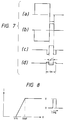
- Fig. 8 is a schematic illustration of the relationship between the light transmissivity of a ferroelectric liquid crystal device and the amplitude of a switching pulse applied to the device. More specifically, a single shot of pulse of a given polarity was applied to the cell (device) which was initially in a complete light-interrupting (black) state so as to change the light-transmissivity of the cell. The light-transmissivity after the application of the single shot of pulse varies according to the amplitude of the pulse. The light-transmissivity I was plotted as a function of the pulse amplitude V, thus, obtaining the curve shown in Fig. 8.
- the light-transmissivity of the cell is not changed when the amplitude V of the pulse applied is below the threshold value V th (V ⁇ V th ) so that the state of light transmission 9(b) is the same as that shown in Fig. 9A obtained in the state before the application of the pulse.
- V th ⁇ V ⁇ V sat portions of the liquid crystal in the pixel are switched to the other stable state, i.e., to the light-transmitting state, as shown in Fig. 9C, so that the pixel exhibits an intermediate level of light transmission.
- the pulse amplitude is further increased to exceed the threshold level (V sat ⁇ V)
- the entire portion of the pixel is switched to light-transmitting state, thus achieving a constant light transmissivity.
- a stable analog gradation display could be performed despite any variation in the threshold characteristics in the display area due to variation in temperature or cell thickness, by using the described area modulation method in combination with a driving method which is disclosed, for example, in the specification of Japanese Patent Application No. 3-73127 of the same applicant.
- This driving method will be referred to as "driving method of prior application” hereinafter.
- the driving method of the prior application essentially requires that four writing pulses and auxiliary pulses assisting these writing pulses are used for each pixel, in order to compensate for any fluctuation in the threshold characteristics in the display area. Consequently, an impractically long time, which is about 10 times as long as that required for conventional monochromatic binary display, is required for writing information in the display area.
- an object of the present invention is to provide a display apparatus which can perform a prompt display of an image with gradation, while compensating for any variation in the threshold value within the display area attributable to fluctuation in the temperature and cell thickness in the display area.
- a display apparatus in which each of pixels is composed of first and second bi-stable sub-pixels having the same threshold characteristics.
- a first writing pulse is applied to the first sub-pixel so as to completely set it to the first stable state, followed by application of a second writing pulse to write the second stable state in the first sub-pixel, while a first writing pulse is applied to the second sub-pixel to completely set it into the second stable state followed by application of a second writing pulse to write the first stable state in the second sub-pixel.
- the display apparatus employs a multiplicity of pixels each of which is composed of first and second bi-stable sub-pixels having the same threshold characteristics.
- a first writing pulse is applied to the first sub-pixel so as to completely set it to the first stable state, followed by application of a second and subsequent writing pulses to alternately write the second stable state and the first stable state in the first sub-pixel, while a first writing pulse is applied to the second sub-pixel to completely set it into the second stable state followed by application of a second and subsequent writing pulses to alternately write the first stable state and the second stable state in the second sub-pixel.
- a pixel P1 is composed of a pair of sub-pixels A and B, while another pixel P2 is composed of a pair of sub-pixels A′ and B′, as shown in Fig. 1C. It is also assumed that the pixels P1 and P2 have different threshold characteristics as shown in Fig. 1A. More specifically, in Fig. 1A, a curve a shows the threshold characteristic exhibited by the pixel P1 when a white writing pulse is applied thereto, while a curve b shows the threshold characteristic exhibited by the same pixel P1 when a black writing pulse is applied thereto.
- a curve a′ shows the threshold characteristic exhibited by the pixel P2 when a white writing pulse is applied thereto
- a curve b′ shows the threshold characteristic exhibited by the same pixel P2 when a black writing pulse is applied thereto.
- a symbol V th indicates the threshold voltage for the threshold characteristics a and b
- V sat indicates the saturation voltage for the threshold characteristics a and b .
- Light transmissivity 0 % indicates that a sub-pixel is in completely light-interrupting or black state
- light-transmissivity 100 % indicates that the sub-pixel is in a completely light-transmitting or white state.
- Pulses of a waveform S A shown in Fig. 1B is applied to the sub-pixels A and A′ while the sub-pixels B and B′ receive pulses of a waveform S B shown in Fig. 1B.
- the waveform S A is composed of a pulse A1 and a pulse A2.
- the sub-pixel A is changed into completely black state, i.e., to transmissivity 0 %, in response to the black writing pulse A1 and is changed to and maintained at a transmissivity ⁇ % in response to a white writing pulse A2.
- the waveform S B is composed of a pulse B1 and a pulse B2.
- the sub-pixel B is changed into completely white state, i.e., to transmissivity 100 %, in response to the white writing pulse B1 and is changed to and maintained at a transmissivity ⁇ % in response to a black writing pulse B2. Consequently, the pixel P1 exhibits a halftone of ⁇ % in terms of transmissivity as shown in Fig. 1C.
- the sub-pixel A′ is changed into completely black state, i.e., to transmissivity 0 %, in response to the black writing pulse A1 and is changed to and maintained at a transmissivily ⁇ + ⁇ % in response to a white writing pulse A2.
- the sub-pixel B′ is changed into completely white state, i.e., to transmissivity 100 %, in response to the white writing pulse B1 and is changed to and maintained at a transmissivity ⁇ - ⁇ % in response to a black writing pulse B2. Consequently, the pixel P2 also exhibits a halftone of ⁇ % in terms of transmissivity as shown in Fig. 1C.
- the condition (4) requires that, when the display apparatus has a transmissivity variation of b %, it is possible to uniformly display an image with a gradation within the range between b % and (100 - b) %. For instance, when the display apparatus has a transmissivity variation of 10 %, it is possible to display an image with analog gradation varying between 10 and 90 % in terms of transmissivity. It is also possible to display an image with a digital gradation which varies in a stepped manner at a pitch of 10 % in terms of transmissivity. When the display is conducted in digital manner, the threshold characteristics need not be linear but may be stepped as shown in Fig. 10.
- the gradation is formed by varying the voltage of the driving signals. This, however, is only illustrative and the same effect can be attained by varying the amplitude of the driving pulses while fixing the voltage.
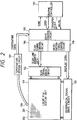
- Fig. 2 shows a liquid crystal display apparatus in accordance with an embodiment of the present invention.
- This display apparatus has a liquid crystal display unit having an electrode matrix composed of scanning electrodes 201 and information electrodes 202 which are detailed in Fig. 3, an information signal drive circuit 103 for applying information signals to the liquid crystal through the information electrodes 202, a scan signal drive circuit 102 for applying scan signals to the liquid crystal through the scanning electrodes 201, a scan signal control circuit 104, an information signal control circuit 106, a drive control circuit 105, a thermistor 108 for detecting the temperature of the display unit 101, and a temperature sensor circuit 109 for sensing the temperature of the display unit 1-1 on the basis of the output of the thermistor 108.
- a ferroelectric liquid crystal is positioned between the scanning electrode 201 and the information electrode 202.
- Numeral 107 denotes a graphic controller which supplies data to the scan signal control circuit 104 and the information signal control circuit 106 through the drive control circuit 105 so as to be converted into address data and display data.
- the temperature of the liquid crystal display unit 101 is delivered to the temperature sensor circuit 109 through the thermistor 108 the output of which is delivered as temperature data to the scan signal control circuit 104 through the drive control circuit 105.
- the scan signal drive circuit 102 generates a scan signal in accordance with the address data and the temperature data and applies the scan signal to the scanning electrodes 201 of the liquid crystal display unit 101.
- the information signal drive circuit 103 generates information signal in accordance with the display data and applies the same to the information electrodes 202 of the liquid crystal display unit 101.
- numerals 203 and 204 denote sub-pixels which are formed at the points where the scanning electrodes 201 and the information electrodes 202 cross each other. These two sub-pixels 203 and 204 in combination form a pixel which is an element of the display.
- Fig. 4 is a fragmentary sectional view of the liquid crystal display unit 101.
- An analyzer 301 and a polarizer 306 are arranged in a cross-nicol relation to each other.
- Numerals 302 and 305 denote glass substrates
- 303 denotes a layer of the ferroelectric liquid crystal
- 304 denotes a UV set resin
- 307 denotes a spacer.
- Figs. 5(a) to 5(c) show waveforms of drive signals employed in the apparatus shown in Fig. 2. More specifically, Fig. 5(a) shows a selection signal which is generated by the scan signal drive circuit 102 and applied to the first sub-pixel, Fig. 5(b) shows a selection signal applied to the second sub-pixel by the scan signal drive circuit 102 in synchronization with the signal of Fig. 5(a), and Fig. 5(c) represents an information signal which is produced by the information signal drive circuit 103 and which has an amplitude corresponding to the gradation data.
- the time 1H required for driving one pixel for display is as short as 4 times the width of the second pulse, i.e., 4 ⁇ t.
- the gradation display is performed by varying the amplitude of the pulse while fixing the width of the pulse, this is only illustrative and an equivalent effect can be obtained by varying the pulse width while fixing the amplitude of the pulse.
- a gradient is imparted to the cell thickness in order to obtain a gentle threshold characteristics in the pixel.
- This is not exclusive and an equivalent effect can be obtained by using an alternative measure such as gradient of capacitance or a gradient of electrical potential of the electrode.
- Fig. 6 shows an embodiment having an electrode structure which is different from that of the embodiment described above. Namely, while in the embodiment shown in Fig. 3 the pair of sub-pixels 203 and 204 are formed on the points where two different scanning electrodes 201, 201 cross a common information electrode 202, to sub-pixels in the embodiment shown in Fig. 6 belong to different scanning electrodes 601 and different information electrodes 602.
- Figs. 7(a) to 7(d) show waveforms of drive signals used in this embodiment. More specifically, Fig. 7(a) shows the waveform of the scan selection signal applied to the first sub-pixel, Fig. 7(b) shows the waveform of the scan selection signal applied to the second sub-pixel, Figs.
- FIG. 7(c) and 7(d) show, respectively, the waveforms of information signals applied to the first and second sub-pixels.
- the time 1H required for one pixel to perform display is as small as twice that of the width of the second writing pulse, i.e., 2 ⁇ t, which is the same as that required for conventional monochromatic binary display and half the time required in the embodiment shown in Fig. 3.
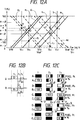
- a display area contains pixels P A , P B , P C , P D and P E which are respectively composed of two sub-pixels A1, A2, B1, B2, C1, C2, D1, D2 and E1, E2.
- the pixel P A has the highest threshold level among the pixels and other pixels P B , P C , P D and P E have threshold value decreasing in the mentioned order.
- a1 and a2 represent the threshold characteristics for white writing pulse and black writing pulse for the pixel P A
- b1 and b2 represent the threshold characteristics for white writing pulse and black writing pulse for the pixel P B
- c1 and c2 represent the threshold characteristics for white writing pulse and black writing pulse for the pixel P C
- d1 and d2 represent the threshold characteristics for white writing pulse and black writing pulse for the pixel P D
- e1 and e2 represent the threshold characteristics for white writing pulse and black writing pulse for the pixel P E , respectively.
- V th represents the threshold voltage of the threshold characteristics a1, a2
- V sat represents the saturation voltage of the threshold characteristics a1, a2.
- V th ′ represents the threshold voltage of the threshold characteristics e1, e2, while V sat ′ represents the saturation voltage of the threshold characteristics e1, e2.
- Completely black state of a sub-pixel is represented by transmissivity 0 %, while transmissivity 100 % indicates that the sub-pixel is in completely white state.
- Signals of waveforms Q and R shown in Fig. 12A are applied to the sub-pixels A1 to E1 and sub-pixels A2 to E2, respectively.
- the waveform Q is composed of pulses Q1, Q2 and Q3.
- the pulse Q1 is a black pulse which turns all the pixels into the black state of 0 % in terms of transmissivity
- the pulse Q2 is a white writing pulse which turns the sub-pixel A1 into a state of ⁇ % in terms of transmissivity
- the pulse Q3 is a black writing pulse which realizes the transmissivity of ⁇ % in the sub-pixel E1 whose saturation voltage V sat ′ equals to the threshold voltage V th of the sub-pixel A1.
- the waveform R is composed of pulses R1, R2 and R3.
- the pulse R1 is a white writing pulse which turns all the pixels into the white state of 100 % in terms of transmissivity
- the pulse R2 is a black writing pulse which turns the sub-pixel A2 into a state of ⁇ % in terms of transmissivity
- the pulse R3 is a white writing pulse which realizes the transmissivity of ⁇ % in the sub-pixel E1 whose saturation voltage V sat ′ equals to the threshold voltage V th of the sub-pixel A2.
- the transmissivity of the sub-pixel B1 realized by the pulse Q2 is ⁇ + ⁇ %
- the transmissivity of the sub-pixel B2 created by the pulse R2 is ⁇ - ⁇ %, for the reason stated below.
- the transmissivity of the sub-pixel D1 realized by the pulse Q3 is ⁇ + ⁇ %
- the transmissivity of the sub-pixel D2 created by the pulse R3 is ⁇ - ⁇ %. This is proved by the fact that the triangles STU and S′T′U′ are congruent to each other.
- adjoint lines are added including a line L which passes the point c and parallel to the line cl, a line L′ passing the point e and parallel to the line cl and a line which is drawn from the point g normally to the voltage axis.
- the triangle abc is congruent to the triangle adc and that the triangle def is congruent to the triangle ghi. Since the triangle abc is congruent to the triangle adc, the lengths of the sides ab and ad are equal to each other and to ⁇ .
- the length of the side ak equals to ⁇ , the length of the side dk is represented by ⁇ + ⁇ .
- the compensation method in accordance with the present invention is valid on the following four conditions:
- the condition (4) is posed when three writing pulses are employed for writing in a single sub-pixel.
- the condition is V th ⁇ 2V sat and, when seven pulses are employed, the condition is V th ⁇ 4V sat .
- compensation is possible when the amount of variation is within 3 times and 5 times, respectively.
- the gradation display is performed by varying the voltage of the pulses applied. This, however, is not essential and the same effect can be obtained when the pulse widths are controlled while the voltages are fixed. Furthermore, when the gradation display is to be performed digitally, it is not always necessary that the threshold characteristics are linear. Namely, in such a case, the threshold characteristics may be stepped as shown in Fig. 10.
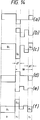
- Figs. 14(a) to 14(f) show waveforms of drive signals employed in the apparatus shown in Fig. 2. More specifically, Fig. 14(a) shows a selection signal which is generated by the scan signal drive circuit 102 and applied to the first sub-pixel, Fig. 14(b) shows an information signal which is produced by the information signal drive circuit 103 and which has an amplitude corresponding to the gradation data. Fig. 14(c) shows a composite waveform composed of the waveforms of Figs. 14(a) and 14(b). Fig. 14(d) shows the waveform of the selection signal which is applied to the second sub-pixel by the scan signal drive circuit 102. Fig.
- FIG. 14(e) shows the waveform of information signal which is applied to the second sub-pixel by the information signal drive circuit 103 and which has an amplitude corresponding to the gradation data.
- Fig. 14(f) shows the composite waveform composed of the waveforms shown in Figs. 14(d) and 14(e).
- Symbols t1 to t3, Q1 to Q3 and R1 to R3 represent the same pulse widths and pulses as those shown in Fig. 12B.
- the time 1H required for driving one pixel for display is as short as 4 times the width of the second and subsequent writing pulses, i.e., 4 ⁇ t.
- the gradation display is performed by varying the amplitude of the pulse while fixing the width of the pulse, this is only illustrative and an equivalent effect can be obtained by varying the pulse width while fixing the amplitude of the pulse.
- a gradient is imparted to the cell thickness in order to obtain a gentle threshold characteristics in the pixel.
- This is not exclusive and an equivalent effect can be obtained by using an alternative measure such as gradient of capacitance or a gradient of electrical potential of the electrode.
- a display apparatus comprising: a display section having a multiplicity of pixels arranged in the form of a matrix, each pixel having first and second bi-stable sub-pixels which have the same threshold characteristics; and driving means for driving the pixels in such a manner that a first writing pulse is applied to the first sub-pixel so as to write a complete first stable state in the first sub-pixel, followed by application of a second writing pulse to write the second stable state, while a first writing pulse is applied to the second sub-pixel to write a complete second stable state in the second sub-pixel, followed by application of a second writing pulse to write the first stable state.
- a display apparatus comprising: a display section having a multiplicity of pixels arranged in the form of a matrix, each pixel having first and second bi-stable sub-pixels which have the same threshold characteristics; and driving means for driving the pixels in such a manner that a first writing pulse is applied to the first sub-pixel so as to write a complete first stable state in the first sub-pixel, followed by application of
- a A display apparatus comprising: a display section having a multiplicity of pixels arranged in the form of a matrix, each pixel having first and second bi-stable sub-pixels which have the same threshold characteristics; and driving means for driving the pixels by applying a plurality of writing pulses to each of the first and second sub-pixels in such a manner that a first writing pulse is applied to the first sub-pixel so as to write a complete first stable state in the first sub-pixel, followed by application of second and subsequent writing pulses to alternately write the second stable state and the first stable state, while a first writing pulse is applied to the second sub-pixel to write a complete second stable state in the second sub-pixel, followed by application of second and subsequent writing pulses to alternately write the first stable state and the second stable state.
- This arrangement also makes it possible to obtain a prompt display of information with gradation while compensating for any variation in the threshold voltage attributable to variation in the temperature or cell thickness in the display unit.
Landscapes
- Engineering & Computer Science (AREA)
- Theoretical Computer Science (AREA)
- Physics & Mathematics (AREA)
- Crystallography & Structural Chemistry (AREA)
- Computer Hardware Design (AREA)
- General Physics & Mathematics (AREA)
- Chemical & Material Sciences (AREA)
- Liquid Crystal Display Device Control (AREA)
- Navigation (AREA)
- Control Of Indicators Other Than Cathode Ray Tubes (AREA)
- Devices For Checking Fares Or Tickets At Control Points (AREA)
- Optical Communication System (AREA)
- Traffic Control Systems (AREA)
- Control Of El Displays (AREA)
Applications Claiming Priority (4)
| Application Number | Priority Date | Filing Date | Title |
|---|---|---|---|
| JP20618891A JP2766947B2 (ja) | 1991-07-24 | 1991-07-24 | 表示装置 |
| JP206189/91 | 1991-07-24 | ||
| JP206188/91 | 1991-07-24 | ||
| JP03206189A JP3082149B2 (ja) | 1991-07-24 | 1991-07-24 | 表示装置 |
Publications (3)
| Publication Number | Publication Date |
|---|---|
| EP0526095A2 true EP0526095A2 (de) | 1993-02-03 |
| EP0526095A3 EP0526095A3 (en) | 1993-09-01 |
| EP0526095B1 EP0526095B1 (de) | 1997-05-21 |
Family
ID=26515483
Family Applications (1)
| Application Number | Title | Priority Date | Filing Date |
|---|---|---|---|
| EP92306719A Expired - Lifetime EP0526095B1 (de) | 1991-07-24 | 1992-07-23 | Datenanzeige |
Country Status (5)
| Country | Link |
|---|---|
| US (1) | US5654732A (de) |
| EP (1) | EP0526095B1 (de) |
| AT (1) | ATE153469T1 (de) |
| DE (1) | DE69219828T2 (de) |
| ES (1) | ES2101036T3 (de) |
Cited By (4)
| Publication number | Priority date | Publication date | Assignee | Title |
|---|---|---|---|---|
| EP0867855A1 (de) * | 1997-03-25 | 1998-09-30 | Sharp Kabushiki Kaisha | Grauskala-Ansteuerungsverfahren für Flüssigkristallanzeige, wobei die Effekte der Temperaturänderung kompensiert werden |
| EP0791848A3 (de) * | 1996-02-20 | 1998-10-28 | Sharp Kabushiki Kaisha | Anzeige und ihr Ansteuerungsverfahren |
| EP0886258A1 (de) * | 1997-06-20 | 1998-12-23 | Sharp Kabushiki Kaisha | Ferroelektrische Flüssigkristallanzeige und Verfahren zur Adressierung einer feroelektrischen Flüssigkristallanzeige |
| EP0911794A1 (de) * | 1997-10-16 | 1999-04-28 | Sharp Kabushiki Kaisha | Anzeigeeinrichtung und Steuerungsverfahren dafür mit gleichzeitiger Adressierung von Abtastelektrodengruppen und Datenelektrodenpaaren in Kombination |
Families Citing this family (32)
| Publication number | Priority date | Publication date | Assignee | Title |
|---|---|---|---|---|
| JPH07152017A (ja) * | 1993-11-30 | 1995-06-16 | Sony Corp | 液晶素子の駆動方法及びその液晶素子 |
| TW295652B (de) * | 1994-10-24 | 1997-01-11 | Handotai Energy Kenkyusho Kk | |
| US7193625B2 (en) | 1999-04-30 | 2007-03-20 | E Ink Corporation | Methods for driving electro-optic displays, and apparatus for use therein |
| US7999787B2 (en) | 1995-07-20 | 2011-08-16 | E Ink Corporation | Methods for driving electrophoretic displays using dielectrophoretic forces |
| US5734365A (en) * | 1996-01-25 | 1998-03-31 | Canon Kabushiki Kaisha | Liquid crystal display apparatus |
| JP3542504B2 (ja) | 1997-08-28 | 2004-07-14 | キヤノン株式会社 | カラー表示装置 |
| US7012600B2 (en) | 1999-04-30 | 2006-03-14 | E Ink Corporation | Methods for driving bistable electro-optic displays, and apparatus for use therein |
| US7119772B2 (en) | 1999-04-30 | 2006-10-10 | E Ink Corporation | Methods for driving bistable electro-optic displays, and apparatus for use therein |
| JP2001242828A (ja) * | 2000-02-25 | 2001-09-07 | Internatl Business Mach Corp <Ibm> | 多階調表現のための画像表示装置、液晶表示装置、および画像表示方法 |
| US6917349B2 (en) * | 2001-02-28 | 2005-07-12 | Intel Corporation | Displaying information on passive storage medium |
| US7023457B2 (en) * | 2001-03-13 | 2006-04-04 | Intel Corporation | System and method for intensity control of a pixel |
| US7952557B2 (en) | 2001-11-20 | 2011-05-31 | E Ink Corporation | Methods and apparatus for driving electro-optic displays |
| US8125501B2 (en) | 2001-11-20 | 2012-02-28 | E Ink Corporation | Voltage modulated driver circuits for electro-optic displays |
| US8593396B2 (en) | 2001-11-20 | 2013-11-26 | E Ink Corporation | Methods and apparatus for driving electro-optic displays |
| US7528822B2 (en) | 2001-11-20 | 2009-05-05 | E Ink Corporation | Methods for driving electro-optic displays |
| US9412314B2 (en) | 2001-11-20 | 2016-08-09 | E Ink Corporation | Methods for driving electro-optic displays |
| US9530363B2 (en) | 2001-11-20 | 2016-12-27 | E Ink Corporation | Methods and apparatus for driving electro-optic displays |
| US8558783B2 (en) | 2001-11-20 | 2013-10-15 | E Ink Corporation | Electro-optic displays with reduced remnant voltage |
| CN102789764B (zh) * | 2001-11-20 | 2015-05-27 | 伊英克公司 | 驱动双稳态电光显示器的方法 |
| US7466319B1 (en) * | 2002-01-08 | 2008-12-16 | 3Dlabs | System and method for fast gradient pixel clears in graphics rendering |
| US20080024482A1 (en) * | 2002-06-13 | 2008-01-31 | E Ink Corporation | Methods for driving electro-optic displays |
| JP4248306B2 (ja) * | 2002-06-17 | 2009-04-02 | シャープ株式会社 | 液晶表示装置 |
| US20130063333A1 (en) | 2002-10-16 | 2013-03-14 | E Ink Corporation | Electrophoretic displays |
| US10726798B2 (en) | 2003-03-31 | 2020-07-28 | E Ink Corporation | Methods for operating electro-optic displays |
| US8174490B2 (en) | 2003-06-30 | 2012-05-08 | E Ink Corporation | Methods for driving electrophoretic displays |
| EP2698784B1 (de) | 2003-08-19 | 2017-11-01 | E Ink Corporation | Elektrooptischer Bildschirm |
| US8928562B2 (en) | 2003-11-25 | 2015-01-06 | E Ink Corporation | Electro-optic displays, and methods for driving same |
| US7492339B2 (en) | 2004-03-26 | 2009-02-17 | E Ink Corporation | Methods for driving bistable electro-optic displays |
| US11250794B2 (en) | 2004-07-27 | 2022-02-15 | E Ink Corporation | Methods for driving electrophoretic displays using dielectrophoretic forces |
| US7453445B2 (en) | 2004-08-13 | 2008-11-18 | E Ink Corproation | Methods for driving electro-optic displays |
| US20070103412A1 (en) * | 2005-11-09 | 2007-05-10 | Pao-Yun Tang | Liquid crystal display having a voltage divider with a thermistor |
| KR101793352B1 (ko) | 2010-04-09 | 2017-11-02 | 이 잉크 코포레이션 | 전기광학 디스플레이의 구동 방법 |
Family Cites Families (10)
| Publication number | Priority date | Publication date | Assignee | Title |
|---|---|---|---|---|
| US4661809A (en) * | 1982-05-05 | 1987-04-28 | Litton Systems, Inc. | Magneto-optic chip with gray-scale capability |
| CH666560A5 (de) * | 1983-03-01 | 1988-07-29 | Tadeusz Bobak | Anzeigevorrichtung. |
| JPS60218626A (ja) * | 1984-04-13 | 1985-11-01 | Sharp Corp | カラ−液晶表示装置 |
| JPS6194023A (ja) * | 1984-10-15 | 1986-05-12 | Canon Inc | 液晶素子 |
| GB2173336B (en) * | 1985-04-03 | 1988-04-27 | Stc Plc | Addressing liquid crystal cells |
| GB8808812D0 (en) * | 1988-04-14 | 1988-05-18 | Emi Plc Thorn | Display device |
| JP2826744B2 (ja) * | 1989-03-02 | 1998-11-18 | キヤノン株式会社 | 液晶表示装置 |
| JPH0373127A (ja) * | 1989-08-12 | 1991-03-28 | Olympus Optical Co Ltd | 内視鏡鉗子栓及び内視鏡鉗子栓用アダプタ |
| NL9000942A (nl) * | 1990-04-20 | 1991-11-18 | Philips Nv | Weergeefinrichting. |
| JP2915104B2 (ja) * | 1990-07-30 | 1999-07-05 | キヤノン株式会社 | 液晶素子および液晶駆動方法 |
-
1992
- 1992-07-23 DE DE69219828T patent/DE69219828T2/de not_active Expired - Fee Related
- 1992-07-23 EP EP92306719A patent/EP0526095B1/de not_active Expired - Lifetime
- 1992-07-23 ES ES92306719T patent/ES2101036T3/es not_active Expired - Lifetime
- 1992-07-23 AT AT92306719T patent/ATE153469T1/de not_active IP Right Cessation
-
1995
- 1995-01-03 US US08/367,772 patent/US5654732A/en not_active Expired - Fee Related
Cited By (9)
| Publication number | Priority date | Publication date | Assignee | Title |
|---|---|---|---|---|
| EP0791848A3 (de) * | 1996-02-20 | 1998-10-28 | Sharp Kabushiki Kaisha | Anzeige und ihr Ansteuerungsverfahren |
| US6061043A (en) * | 1996-02-20 | 2000-05-09 | Sharp Kabushiki Kaisha | Liquid crystal display having grey levels with reduced variations due to temperature and liquid crystal variations |
| US6075506A (en) * | 1996-02-20 | 2000-06-13 | Sharp Kabushiki Kaisha | Display and method of operating a display |
| EP0867855A1 (de) * | 1997-03-25 | 1998-09-30 | Sharp Kabushiki Kaisha | Grauskala-Ansteuerungsverfahren für Flüssigkristallanzeige, wobei die Effekte der Temperaturänderung kompensiert werden |
| US6232943B1 (en) | 1997-03-25 | 2001-05-15 | Sharp Kabushiki Kaisha | Liquid crystal display |
| EP0886258A1 (de) * | 1997-06-20 | 1998-12-23 | Sharp Kabushiki Kaisha | Ferroelektrische Flüssigkristallanzeige und Verfahren zur Adressierung einer feroelektrischen Flüssigkristallanzeige |
| US6137463A (en) * | 1997-06-20 | 2000-10-24 | Sharp Kabushiki Kaisha | Liquid crystal device and method of addressing a liquid crystal device |
| EP0911794A1 (de) * | 1997-10-16 | 1999-04-28 | Sharp Kabushiki Kaisha | Anzeigeeinrichtung und Steuerungsverfahren dafür mit gleichzeitiger Adressierung von Abtastelektrodengruppen und Datenelektrodenpaaren in Kombination |
| US6281866B1 (en) | 1997-10-16 | 2001-08-28 | Sharp Kabushiki Kaisha | Display device and a method of addressing a display device |
Also Published As
| Publication number | Publication date |
|---|---|
| EP0526095B1 (de) | 1997-05-21 |
| US5654732A (en) | 1997-08-05 |
| ES2101036T3 (es) | 1997-07-01 |
| DE69219828T2 (de) | 1997-10-16 |
| DE69219828D1 (de) | 1997-06-26 |
| EP0526095A3 (en) | 1993-09-01 |
| ATE153469T1 (de) | 1997-06-15 |
Similar Documents
| Publication | Publication Date | Title |
|---|---|---|
| EP0526095B1 (de) | Datenanzeige | |
| EP0618562B1 (de) | Anzeigevorrichtung und Steuerverfahren für Anzeigevorrichtung | |
| US5508711A (en) | Liquid crystal display apparatus and driving method of such apparatus | |
| US20160314749A1 (en) | Methods for driving electro-optic displays | |
| EP0256548B1 (de) | Verfahren und Vorrichtung zur Ansteuerung einer optischen Modulationsanordnung | |
| US20050024353A1 (en) | Methods for driving electro-optic displays | |
| KR0148246B1 (ko) | 액정 장치의 구동 방법 | |
| EP0510606B1 (de) | Flüssigkristallanzeigevorrichtung | |
| EP2916312A1 (de) | Verfahren zur ansteuerung bistabiler elektro-optischer anzeigen | |
| US5805130A (en) | Liquid crystal display device and method for driving the same | |
| JP2759589B2 (ja) | 強誘電性液晶表示素子 | |
| EP0238287B1 (de) | Elektro-optische Vorrichtung mit ferroelektrischem Flüssigkristall | |
| EP0692779B1 (de) | Verfahren zur Steuerung einer Anzeigetafel | |
| EP0526713B1 (de) | Flüssigkristallanzeigegerät mit aktiver Matrix | |
| JP2766947B2 (ja) | 表示装置 | |
| US6069603A (en) | Method of driving a matrix display device | |
| JP3082149B2 (ja) | 表示装置 | |
| JPH0854605A (ja) | 反強誘電性液晶ディスプレイの駆動方法 | |
| US6215533B1 (en) | Ferroelectric liquid crystal driving using square wave and non-square wave signals | |
| US5748162A (en) | Low voltage liquid crystal display device | |
| JP3101790B2 (ja) | 液晶表示素子 | |
| CN1386260A (zh) | 一种液晶显示设备和用一组扫描线的主动寻址和通过基于帧持续时间的非二进制划分的时间调制而得到的等级来驱动该液晶显示设备的方法 | |
| JP3096877B2 (ja) | 液晶素子の駆動法 | |
| JP3035404B2 (ja) | 表示装置 | |
| KR100343381B1 (ko) | 액정 표시 장치 |
Legal Events
| Date | Code | Title | Description |
|---|---|---|---|
| PUAI | Public reference made under article 153(3) epc to a published international application that has entered the european phase |
Free format text: ORIGINAL CODE: 0009012 |
|
| AK | Designated contracting states |
Kind code of ref document: A2 Designated state(s): AT BE CH DE DK ES FR GB GR IT LI LU NL PT SE |
|
| PUAL | Search report despatched |
Free format text: ORIGINAL CODE: 0009013 |
|
| AK | Designated contracting states |
Kind code of ref document: A3 Designated state(s): AT BE CH DE DK ES FR GB GR IT LI LU NL PT SE |
|
| 17P | Request for examination filed |
Effective date: 19940118 |
|
| 17Q | First examination report despatched |
Effective date: 19950301 |
|
| GRAG | Despatch of communication of intention to grant |
Free format text: ORIGINAL CODE: EPIDOS AGRA |
|
| GRAH | Despatch of communication of intention to grant a patent |
Free format text: ORIGINAL CODE: EPIDOS IGRA |
|
| GRAH | Despatch of communication of intention to grant a patent |
Free format text: ORIGINAL CODE: EPIDOS IGRA |
|
| GRAA | (expected) grant |
Free format text: ORIGINAL CODE: 0009210 |
|
| AK | Designated contracting states |
Kind code of ref document: B1 Designated state(s): AT BE CH DE DK ES FR GB GR IT LI LU NL PT SE |
|
| PG25 | Lapsed in a contracting state [announced via postgrant information from national office to epo] |
Ref country code: LI Effective date: 19970521 Ref country code: GR Free format text: LAPSE BECAUSE OF FAILURE TO SUBMIT A TRANSLATION OF THE DESCRIPTION OR TO PAY THE FEE WITHIN THE PRESCRIBED TIME-LIMIT Effective date: 19970521 Ref country code: DK Effective date: 19970521 Ref country code: CH Effective date: 19970521 Ref country code: BE Effective date: 19970521 Ref country code: AT Effective date: 19970521 |
|
| REF | Corresponds to: |
Ref document number: 153469 Country of ref document: AT Date of ref document: 19970615 Kind code of ref document: T |
|
| REG | Reference to a national code |
Ref country code: CH Ref legal event code: EP |
|
| REF | Corresponds to: |
Ref document number: 69219828 Country of ref document: DE Date of ref document: 19970626 |
|
| REG | Reference to a national code |
Ref country code: ES Ref legal event code: FG2A Ref document number: 2101036 Country of ref document: ES Kind code of ref document: T3 |
|
| ET | Fr: translation filed | ||
| PG25 | Lapsed in a contracting state [announced via postgrant information from national office to epo] |
Ref country code: LU Free format text: LAPSE BECAUSE OF NON-PAYMENT OF DUE FEES Effective date: 19970723 |
|
| PG25 | Lapsed in a contracting state [announced via postgrant information from national office to epo] |
Ref country code: PT Effective date: 19970821 |
|
| REG | Reference to a national code |
Ref country code: CH Ref legal event code: PL |
|
| PLBE | No opposition filed within time limit |
Free format text: ORIGINAL CODE: 0009261 |
|
| STAA | Information on the status of an ep patent application or granted ep patent |
Free format text: STATUS: NO OPPOSITION FILED WITHIN TIME LIMIT |
|
| 26N | No opposition filed | ||
| REG | Reference to a national code |
Ref country code: GB Ref legal event code: IF02 |
|
| PGFP | Annual fee paid to national office [announced via postgrant information from national office to epo] |
Ref country code: NL Payment date: 20020731 Year of fee payment: 11 |
|
| PGFP | Annual fee paid to national office [announced via postgrant information from national office to epo] |
Ref country code: ES Payment date: 20030701 Year of fee payment: 12 |
|
| PGFP | Annual fee paid to national office [announced via postgrant information from national office to epo] |
Ref country code: GB Payment date: 20030709 Year of fee payment: 12 |
|
| PGFP | Annual fee paid to national office [announced via postgrant information from national office to epo] |
Ref country code: SE Payment date: 20030717 Year of fee payment: 12 |
|
| PGFP | Annual fee paid to national office [announced via postgrant information from national office to epo] |
Ref country code: FR Payment date: 20030721 Year of fee payment: 12 |
|
| PGFP | Annual fee paid to national office [announced via postgrant information from national office to epo] |
Ref country code: DE Payment date: 20030723 Year of fee payment: 12 |
|
| PG25 | Lapsed in a contracting state [announced via postgrant information from national office to epo] |
Ref country code: NL Free format text: LAPSE BECAUSE OF NON-PAYMENT OF DUE FEES Effective date: 20040201 |
|
| NLV4 | Nl: lapsed or anulled due to non-payment of the annual fee |
Effective date: 20040201 |
|
| PG25 | Lapsed in a contracting state [announced via postgrant information from national office to epo] |
Ref country code: GB Free format text: LAPSE BECAUSE OF NON-PAYMENT OF DUE FEES Effective date: 20040723 |
|
| PG25 | Lapsed in a contracting state [announced via postgrant information from national office to epo] |
Ref country code: SE Free format text: LAPSE BECAUSE OF NON-PAYMENT OF DUE FEES Effective date: 20040724 Ref country code: ES Free format text: LAPSE BECAUSE OF NON-PAYMENT OF DUE FEES Effective date: 20040724 |
|
| PG25 | Lapsed in a contracting state [announced via postgrant information from national office to epo] |
Ref country code: DE Free format text: LAPSE BECAUSE OF NON-PAYMENT OF DUE FEES Effective date: 20050201 |
|
| EUG | Se: european patent has lapsed | ||
| GBPC | Gb: european patent ceased through non-payment of renewal fee |
Effective date: 20040723 |
|
| PG25 | Lapsed in a contracting state [announced via postgrant information from national office to epo] |
Ref country code: FR Free format text: LAPSE BECAUSE OF NON-PAYMENT OF DUE FEES Effective date: 20050331 |
|
| REG | Reference to a national code |
Ref country code: FR Ref legal event code: ST |
|
| PG25 | Lapsed in a contracting state [announced via postgrant information from national office to epo] |
Ref country code: IT Free format text: LAPSE BECAUSE OF NON-PAYMENT OF DUE FEES;WARNING: LAPSES OF ITALIAN PATENTS WITH EFFECTIVE DATE BEFORE 2007 MAY HAVE OCCURRED AT ANY TIME BEFORE 2007. THE CORRECT EFFECTIVE DATE MAY BE DIFFERENT FROM THE ONE RECORDED. Effective date: 20050723 |
|
| REG | Reference to a national code |
Ref country code: ES Ref legal event code: FD2A Effective date: 20040724 |