EP0526237B1 - Appareil de traitement de l'information et substrat d'électrode et milieu de réception de l'information appliquer à l'appareil - Google Patents
Appareil de traitement de l'information et substrat d'électrode et milieu de réception de l'information appliquer à l'appareil Download PDFInfo
- Publication number
- EP0526237B1 EP0526237B1 EP92307006A EP92307006A EP0526237B1 EP 0526237 B1 EP0526237 B1 EP 0526237B1 EP 92307006 A EP92307006 A EP 92307006A EP 92307006 A EP92307006 A EP 92307006A EP 0526237 B1 EP0526237 B1 EP 0526237B1
- Authority
- EP
- European Patent Office
- Prior art keywords
- medium
- electrode
- substrate
- information
- recording medium
- Prior art date
- Legal status (The legal status is an assumption and is not a legal conclusion. Google has not performed a legal analysis and makes no representation as to the accuracy of the status listed.)
- Expired - Lifetime
Links
- 239000000758 substrate Substances 0.000 title claims abstract description 159
- 230000010365 information processing Effects 0.000 title claims abstract description 29
- 239000000523 sample Substances 0.000 claims abstract description 97
- 239000013078 crystal Substances 0.000 claims abstract description 75
- 239000006185 dispersion Substances 0.000 claims abstract description 28
- 229910000510 noble metal Inorganic materials 0.000 claims abstract description 14
- 238000003672 processing method Methods 0.000 claims abstract description 9
- 238000002441 X-ray diffraction Methods 0.000 claims abstract description 6
- 230000003446 memory effect Effects 0.000 claims description 6
- 150000002894 organic compounds Chemical class 0.000 claims description 6
- 230000001747 exhibiting effect Effects 0.000 abstract description 5
- 239000010931 gold Substances 0.000 description 76
- 229910052737 gold Inorganic materials 0.000 description 73
- PCHJSUWPFVWCPO-UHFFFAOYSA-N gold Chemical compound [Au] PCHJSUWPFVWCPO-UHFFFAOYSA-N 0.000 description 72
- 239000010408 film Substances 0.000 description 60
- 238000000034 method Methods 0.000 description 47
- 239000000463 material Substances 0.000 description 26
- XUIMIQQOPSSXEZ-UHFFFAOYSA-N Silicon Chemical compound [Si] XUIMIQQOPSSXEZ-UHFFFAOYSA-N 0.000 description 21
- 229910052710 silicon Inorganic materials 0.000 description 21
- 239000010703 silicon Substances 0.000 description 21
- 238000002474 experimental method Methods 0.000 description 19
- 238000000151 deposition Methods 0.000 description 18
- 230000008021 deposition Effects 0.000 description 17
- 238000007254 oxidation reaction Methods 0.000 description 15
- 239000000243 solution Substances 0.000 description 15
- 230000015654 memory Effects 0.000 description 13
- XLYOFNOQVPJJNP-UHFFFAOYSA-N water Substances O XLYOFNOQVPJJNP-UHFFFAOYSA-N 0.000 description 13
- 150000002500 ions Chemical class 0.000 description 12
- 238000005530 etching Methods 0.000 description 11
- 238000001704 evaporation Methods 0.000 description 11
- 229920001721 polyimide Polymers 0.000 description 11
- ZCYVEMRRCGMTRW-UHFFFAOYSA-N 7553-56-2 Chemical compound [I] ZCYVEMRRCGMTRW-UHFFFAOYSA-N 0.000 description 10
- 238000002425 crystallisation Methods 0.000 description 10
- 230000008025 crystallization Effects 0.000 description 10
- 229910052740 iodine Inorganic materials 0.000 description 10
- 239000011630 iodine Substances 0.000 description 10
- 239000004642 Polyimide Substances 0.000 description 9
- 230000008020 evaporation Effects 0.000 description 9
- 230000003647 oxidation Effects 0.000 description 9
- 230000015572 biosynthetic process Effects 0.000 description 8
- 230000000694 effects Effects 0.000 description 8
- 239000012452 mother liquor Substances 0.000 description 8
- NLKNQRATVPKPDG-UHFFFAOYSA-M potassium iodide Substances [K+].[I-] NLKNQRATVPKPDG-UHFFFAOYSA-M 0.000 description 8
- 150000001875 compounds Chemical class 0.000 description 7
- 239000000975 dye Substances 0.000 description 7
- 238000007738 vacuum evaporation Methods 0.000 description 7
- 239000011521 glass Substances 0.000 description 6
- 229920002120 photoresistant polymer Polymers 0.000 description 6
- 238000001228 spectrum Methods 0.000 description 6
- 238000006243 chemical reaction Methods 0.000 description 5
- 239000011651 chromium Substances 0.000 description 5
- 238000010438 heat treatment Methods 0.000 description 5
- 230000002209 hydrophobic effect Effects 0.000 description 5
- 238000005259 measurement Methods 0.000 description 5
- 229910052751 metal Inorganic materials 0.000 description 5
- 239000002184 metal Substances 0.000 description 5
- BASFCYQUMIYNBI-UHFFFAOYSA-N platinum Substances [Pt] BASFCYQUMIYNBI-UHFFFAOYSA-N 0.000 description 5
- -1 polycyclic aromatic compounds Chemical class 0.000 description 5
- 239000010409 thin film Substances 0.000 description 5
- KRHYYFGTRYWZRS-UHFFFAOYSA-N Fluorane Chemical compound F KRHYYFGTRYWZRS-UHFFFAOYSA-N 0.000 description 4
- 229910021417 amorphous silicon Inorganic materials 0.000 description 4
- 239000007864 aqueous solution Substances 0.000 description 4
- 230000008901 benefit Effects 0.000 description 4
- 230000008859 change Effects 0.000 description 4
- 230000005685 electric field effect Effects 0.000 description 4
- 238000005468 ion implantation Methods 0.000 description 4
- 238000010884 ion-beam technique Methods 0.000 description 4
- 238000001020 plasma etching Methods 0.000 description 4
- 230000008569 process Effects 0.000 description 4
- 239000002904 solvent Substances 0.000 description 4
- 239000011550 stock solution Substances 0.000 description 4
- 239000000126 substance Substances 0.000 description 4
- UHOVQNZJYSORNB-UHFFFAOYSA-N Benzene Chemical compound C1=CC=CC=C1 UHOVQNZJYSORNB-UHFFFAOYSA-N 0.000 description 3
- 229910052581 Si3N4 Inorganic materials 0.000 description 3
- HEMHJVSKTPXQMS-UHFFFAOYSA-M Sodium hydroxide Chemical compound [OH-].[Na+] HEMHJVSKTPXQMS-UHFFFAOYSA-M 0.000 description 3
- 239000003638 chemical reducing agent Substances 0.000 description 3
- 238000010276 construction Methods 0.000 description 3
- 238000010586 diagram Methods 0.000 description 3
- 238000004519 manufacturing process Methods 0.000 description 3
- 230000003287 optical effect Effects 0.000 description 3
- 238000000879 optical micrograph Methods 0.000 description 3
- 239000002245 particle Substances 0.000 description 3
- 229910052697 platinum Inorganic materials 0.000 description 3
- 238000005498 polishing Methods 0.000 description 3
- 230000007704 transition Effects 0.000 description 3
- QGKMIGUHVLGJBR-UHFFFAOYSA-M (4z)-1-(3-methylbutyl)-4-[[1-(3-methylbutyl)quinolin-1-ium-4-yl]methylidene]quinoline;iodide Chemical compound [I-].C12=CC=CC=C2N(CCC(C)C)C=CC1=CC1=CC=[N+](CCC(C)C)C2=CC=CC=C12 QGKMIGUHVLGJBR-UHFFFAOYSA-M 0.000 description 2
- HEDRZPFGACZZDS-UHFFFAOYSA-N Chloroform Chemical compound ClC(Cl)Cl HEDRZPFGACZZDS-UHFFFAOYSA-N 0.000 description 2
- VYZAMTAEIAYCRO-UHFFFAOYSA-N Chromium Chemical compound [Cr] VYZAMTAEIAYCRO-UHFFFAOYSA-N 0.000 description 2
- VEXZGXHMUGYJMC-UHFFFAOYSA-N Hydrochloric acid Chemical compound Cl VEXZGXHMUGYJMC-UHFFFAOYSA-N 0.000 description 2
- QIGBRXMKCJKVMJ-UHFFFAOYSA-N Hydroquinone Chemical compound OC1=CC=C(O)C=C1 QIGBRXMKCJKVMJ-UHFFFAOYSA-N 0.000 description 2
- 239000004952 Polyamide Substances 0.000 description 2
- SMWDFEZZVXVKRB-UHFFFAOYSA-N Quinoline Chemical compound N1=CC=CC2=CC=CC=C21 SMWDFEZZVXVKRB-UHFFFAOYSA-N 0.000 description 2
- 230000001133 acceleration Effects 0.000 description 2
- 229910052782 aluminium Inorganic materials 0.000 description 2
- XAGFODPZIPBFFR-UHFFFAOYSA-N aluminium Chemical compound [Al] XAGFODPZIPBFFR-UHFFFAOYSA-N 0.000 description 2
- MWPLVEDNUUSJAV-UHFFFAOYSA-N anthracene Chemical compound C1=CC=CC2=CC3=CC=CC=C3C=C21 MWPLVEDNUUSJAV-UHFFFAOYSA-N 0.000 description 2
- IOJUPLGTWVMSFF-UHFFFAOYSA-N benzothiazole Chemical compound C1=CC=C2SC=NC2=C1 IOJUPLGTWVMSFF-UHFFFAOYSA-N 0.000 description 2
- YKYOUMDCQGMQQO-UHFFFAOYSA-L cadmium dichloride Chemical compound Cl[Cd]Cl YKYOUMDCQGMQQO-UHFFFAOYSA-L 0.000 description 2
- 229910052804 chromium Inorganic materials 0.000 description 2
- 239000004020 conductor Substances 0.000 description 2
- 238000011161 development Methods 0.000 description 2
- 230000018109 developmental process Effects 0.000 description 2
- 238000004090 dissolution Methods 0.000 description 2
- 230000005684 electric field Effects 0.000 description 2
- 238000010894 electron beam technology Methods 0.000 description 2
- VKOBVWXKNCXXDE-UHFFFAOYSA-N icosanoic acid Chemical compound CCCCCCCCCCCCCCCCCCCC(O)=O VKOBVWXKNCXXDE-UHFFFAOYSA-N 0.000 description 2
- 230000006872 improvement Effects 0.000 description 2
- 238000004518 low pressure chemical vapour deposition Methods 0.000 description 2
- 239000011159 matrix material Substances 0.000 description 2
- 125000001434 methanylylidene group Chemical group [H]C#[*] 0.000 description 2
- 239000010445 mica Substances 0.000 description 2
- 229910052618 mica group Inorganic materials 0.000 description 2
- 239000000203 mixture Substances 0.000 description 2
- 238000012544 monitoring process Methods 0.000 description 2
- 239000000178 monomer Substances 0.000 description 2
- 229910052757 nitrogen Inorganic materials 0.000 description 2
- 239000011368 organic material Substances 0.000 description 2
- 230000001590 oxidative effect Effects 0.000 description 2
- 239000012071 phase Substances 0.000 description 2
- 229920002647 polyamide Polymers 0.000 description 2
- 229920000642 polymer Polymers 0.000 description 2
- 238000006116 polymerization reaction Methods 0.000 description 2
- BBEAQIROQSPTKN-UHFFFAOYSA-N pyrene Chemical compound C1=CC=C2C=CC3=CC=CC4=CC=C1C2=C43 BBEAQIROQSPTKN-UHFFFAOYSA-N 0.000 description 2
- 229910052703 rhodium Inorganic materials 0.000 description 2
- 239000010948 rhodium Substances 0.000 description 2
- 239000004065 semiconductor Substances 0.000 description 2
- 238000000926 separation method Methods 0.000 description 2
- HQVNEWCFYHHQES-UHFFFAOYSA-N silicon nitride Chemical compound N12[Si]34N5[Si]62N3[Si]51N64 HQVNEWCFYHHQES-UHFFFAOYSA-N 0.000 description 2
- 238000000859 sublimation Methods 0.000 description 2
- 230000008022 sublimation Effects 0.000 description 2
- 230000005641 tunneling Effects 0.000 description 2
- 229910052727 yttrium Inorganic materials 0.000 description 2
- BCMCBBGGLRIHSE-UHFFFAOYSA-N 1,3-benzoxazole Chemical compound C1=CC=C2OC=NC2=C1 BCMCBBGGLRIHSE-UHFFFAOYSA-N 0.000 description 1
- OKTJSMMVPCPJKN-UHFFFAOYSA-N Carbon Chemical compound [C] OKTJSMMVPCPJKN-UHFFFAOYSA-N 0.000 description 1
- XFXPMWWXUTWYJX-UHFFFAOYSA-N Cyanide Chemical compound N#[C-] XFXPMWWXUTWYJX-UHFFFAOYSA-N 0.000 description 1
- 101000606504 Drosophila melanogaster Tyrosine-protein kinase-like otk Proteins 0.000 description 1
- DFPAKSUCGFBDDF-UHFFFAOYSA-N Nicotinamide Chemical group NC(=O)C1=CC=CN=C1 DFPAKSUCGFBDDF-UHFFFAOYSA-N 0.000 description 1
- KJTLSVCANCCWHF-UHFFFAOYSA-N Ruthenium Chemical compound [Ru] KJTLSVCANCCWHF-UHFFFAOYSA-N 0.000 description 1
- LSNNMFCWUKXFEE-UHFFFAOYSA-N Sulfurous acid Chemical compound OS(O)=O LSNNMFCWUKXFEE-UHFFFAOYSA-N 0.000 description 1
- 239000002253 acid Substances 0.000 description 1
- 230000006978 adaptation Effects 0.000 description 1
- 125000003277 amino group Chemical group 0.000 description 1
- 238000013459 approach Methods 0.000 description 1
- 238000003491 array Methods 0.000 description 1
- 125000003118 aryl group Chemical group 0.000 description 1
- 239000012298 atmosphere Substances 0.000 description 1
- 230000003190 augmentative effect Effects 0.000 description 1
- DMLAVOWQYNRWNQ-UHFFFAOYSA-N azobenzene Chemical compound C1=CC=CC=C1N=NC1=CC=CC=C1 DMLAVOWQYNRWNQ-UHFFFAOYSA-N 0.000 description 1
- 229920001222 biopolymer Polymers 0.000 description 1
- LLCSWKVOHICRDD-UHFFFAOYSA-N buta-1,3-diyne Chemical group C#CC#C LLCSWKVOHICRDD-UHFFFAOYSA-N 0.000 description 1
- 125000003178 carboxy group Chemical group [H]OC(*)=O 0.000 description 1
- 150000001786 chalcogen compounds Chemical class 0.000 description 1
- 230000005465 channeling Effects 0.000 description 1
- 238000003486 chemical etching Methods 0.000 description 1
- 238000009833 condensation Methods 0.000 description 1
- 230000005494 condensation Effects 0.000 description 1
- 238000007796 conventional method Methods 0.000 description 1
- 230000007797 corrosion Effects 0.000 description 1
- 238000005260 corrosion Methods 0.000 description 1
- 150000001923 cyclic compounds Chemical class 0.000 description 1
- 230000007547 defect Effects 0.000 description 1
- 238000001514 detection method Methods 0.000 description 1
- 230000006866 deterioration Effects 0.000 description 1
- 230000002542 deteriorative effect Effects 0.000 description 1
- 229950010007 dimantine Drugs 0.000 description 1
- 238000006073 displacement reaction Methods 0.000 description 1
- 239000007772 electrode material Substances 0.000 description 1
- 238000005516 engineering process Methods 0.000 description 1
- 125000004185 ester group Chemical group 0.000 description 1
- 230000002349 favourable effect Effects 0.000 description 1
- KTWOOEGAPBSYNW-UHFFFAOYSA-N ferrocene Chemical compound [Fe+2].C=1C=C[CH-]C=1.C=1C=C[CH-]C=1 KTWOOEGAPBSYNW-UHFFFAOYSA-N 0.000 description 1
- 239000010419 fine particle Substances 0.000 description 1
- GVEPBJHOBDJJJI-UHFFFAOYSA-N fluoranthrene Natural products C1=CC(C2=CC=CC=C22)=C3C2=CC=CC3=C1 GVEPBJHOBDJJJI-UHFFFAOYSA-N 0.000 description 1
- 230000006870 function Effects 0.000 description 1
- SRCZENKQCOSNAI-UHFFFAOYSA-H gold(3+);trisulfite Chemical compound [Au+3].[Au+3].[O-]S([O-])=O.[O-]S([O-])=O.[O-]S([O-])=O SRCZENKQCOSNAI-UHFFFAOYSA-H 0.000 description 1
- 239000010439 graphite Substances 0.000 description 1
- 229910002804 graphite Inorganic materials 0.000 description 1
- 150000004820 halides Chemical class 0.000 description 1
- 150000002430 hydrocarbons Chemical group 0.000 description 1
- 125000001165 hydrophobic group Chemical group 0.000 description 1
- 125000002887 hydroxy group Chemical group [H]O* 0.000 description 1
- 125000005462 imide group Chemical group 0.000 description 1
- 239000011810 insulating material Substances 0.000 description 1
- PNDPGZBMCMUPRI-UHFFFAOYSA-N iodine Chemical compound II PNDPGZBMCMUPRI-UHFFFAOYSA-N 0.000 description 1
- 229910052741 iridium Inorganic materials 0.000 description 1
- 239000007788 liquid Substances 0.000 description 1
- 239000004973 liquid crystal related substance Substances 0.000 description 1
- 230000007246 mechanism Effects 0.000 description 1
- 239000007769 metal material Substances 0.000 description 1
- 238000012986 modification Methods 0.000 description 1
- 230000004048 modification Effects 0.000 description 1
- 239000002120 nanofilm Substances 0.000 description 1
- QJGQUHMNIGDVPM-UHFFFAOYSA-N nitrogen group Chemical group [N] QJGQUHMNIGDVPM-UHFFFAOYSA-N 0.000 description 1
- 229910052763 palladium Inorganic materials 0.000 description 1
- KDLHZDBZIXYQEI-UHFFFAOYSA-N palladium Substances [Pd] KDLHZDBZIXYQEI-UHFFFAOYSA-N 0.000 description 1
- 125000001997 phenyl group Chemical group [H]C1=C([H])C([H])=C(*)C([H])=C1[H] 0.000 description 1
- IEQIEDJGQAUEQZ-UHFFFAOYSA-N phthalocyanine Chemical compound N1C(N=C2C3=CC=CC=C3C(N=C3C4=CC=CC=C4C(=N4)N3)=N2)=C(C=CC=C2)C2=C1N=C1C2=CC=CC=C2C4=N1 IEQIEDJGQAUEQZ-UHFFFAOYSA-N 0.000 description 1
- 238000007747 plating Methods 0.000 description 1
- 125000003367 polycyclic group Chemical group 0.000 description 1
- 239000002861 polymer material Substances 0.000 description 1
- 150000004032 porphyrins Chemical group 0.000 description 1
- 238000002360 preparation method Methods 0.000 description 1
- 108090000623 proteins and genes Proteins 0.000 description 1
- 102000004169 proteins and genes Human genes 0.000 description 1
- 238000006479 redox reaction Methods 0.000 description 1
- 230000004044 response Effects 0.000 description 1
- MHOVAHRLVXNVSD-UHFFFAOYSA-N rhodium atom Chemical compound [Rh] MHOVAHRLVXNVSD-UHFFFAOYSA-N 0.000 description 1
- 229910052707 ruthenium Inorganic materials 0.000 description 1
- 239000012266 salt solution Substances 0.000 description 1
- 229920006395 saturated elastomer Polymers 0.000 description 1
- 229930195734 saturated hydrocarbon Natural products 0.000 description 1
- 238000001988 small-angle X-ray diffraction Methods 0.000 description 1
- 238000004544 sputter deposition Methods 0.000 description 1
- 238000000992 sputter etching Methods 0.000 description 1
- 125000004079 stearyl group Chemical group [H]C([*])([H])C([H])([H])C([H])([H])C([H])([H])C([H])([H])C([H])([H])C([H])([H])C([H])([H])C([H])([H])C([H])([H])C([H])([H])C([H])([H])C([H])([H])C([H])([H])C([H])([H])C([H])([H])C([H])([H])C([H])([H])[H] 0.000 description 1
- LSNNMFCWUKXFEE-UHFFFAOYSA-L sulfite Chemical compound [O-]S([O-])=O LSNNMFCWUKXFEE-UHFFFAOYSA-L 0.000 description 1
- PCCVSPMFGIFTHU-UHFFFAOYSA-N tetracyanoquinodimethane Chemical class N#CC(C#N)=C1C=CC(=C(C#N)C#N)C=C1 PCCVSPMFGIFTHU-UHFFFAOYSA-N 0.000 description 1
- YNHJECZULSZAQK-UHFFFAOYSA-N tetraphenylporphyrin Chemical compound C1=CC(C(=C2C=CC(N2)=C(C=2C=CC=CC=2)C=2C=CC(N=2)=C(C=2C=CC=CC=2)C2=CC=C3N2)C=2C=CC=CC=2)=NC1=C3C1=CC=CC=C1 YNHJECZULSZAQK-UHFFFAOYSA-N 0.000 description 1
- FHCPAXDKURNIOZ-UHFFFAOYSA-N tetrathiafulvalene Chemical compound S1C=CSC1=C1SC=CS1 FHCPAXDKURNIOZ-UHFFFAOYSA-N 0.000 description 1
- 238000012546 transfer Methods 0.000 description 1
- WFKWXMTUELFFGS-UHFFFAOYSA-N tungsten Chemical compound [W] WFKWXMTUELFFGS-UHFFFAOYSA-N 0.000 description 1
- 229910052721 tungsten Inorganic materials 0.000 description 1
- 239000010937 tungsten Substances 0.000 description 1
- 229930195735 unsaturated hydrocarbon Natural products 0.000 description 1
- 238000001771 vacuum deposition Methods 0.000 description 1
- 239000012808 vapor phase Substances 0.000 description 1
Images




Classifications
-
- G—PHYSICS
- G11—INFORMATION STORAGE
- G11C—STATIC STORES
- G11C13/00—Digital stores characterised by the use of storage elements not covered by groups G11C11/00, G11C23/00, or G11C25/00
- G11C13/0002—Digital stores characterised by the use of storage elements not covered by groups G11C11/00, G11C23/00, or G11C25/00 using resistive RAM [RRAM] elements
- G11C13/0009—RRAM elements whose operation depends upon chemical change
- G11C13/0014—RRAM elements whose operation depends upon chemical change comprising cells based on organic memory material
-
- B—PERFORMING OPERATIONS; TRANSPORTING
- B82—NANOTECHNOLOGY
- B82Y—SPECIFIC USES OR APPLICATIONS OF NANOSTRUCTURES; MEASUREMENT OR ANALYSIS OF NANOSTRUCTURES; MANUFACTURE OR TREATMENT OF NANOSTRUCTURES
- B82Y10/00—Nanotechnology for information processing, storage or transmission, e.g. quantum computing or single electron logic
-
- C—CHEMISTRY; METALLURGY
- C30—CRYSTAL GROWTH
- C30B—SINGLE-CRYSTAL GROWTH; UNIDIRECTIONAL SOLIDIFICATION OF EUTECTIC MATERIAL OR UNIDIRECTIONAL DEMIXING OF EUTECTOID MATERIAL; REFINING BY ZONE-MELTING OF MATERIAL; PRODUCTION OF A HOMOGENEOUS POLYCRYSTALLINE MATERIAL WITH DEFINED STRUCTURE; SINGLE CRYSTALS OR HOMOGENEOUS POLYCRYSTALLINE MATERIAL WITH DEFINED STRUCTURE; AFTER-TREATMENT OF SINGLE CRYSTALS OR A HOMOGENEOUS POLYCRYSTALLINE MATERIAL WITH DEFINED STRUCTURE; APPARATUS THEREFOR
- C30B29/00—Single crystals or homogeneous polycrystalline material with defined structure characterised by the material or by their shape
- C30B29/02—Elements
-
- C—CHEMISTRY; METALLURGY
- C30—CRYSTAL GROWTH
- C30B—SINGLE-CRYSTAL GROWTH; UNIDIRECTIONAL SOLIDIFICATION OF EUTECTIC MATERIAL OR UNIDIRECTIONAL DEMIXING OF EUTECTOID MATERIAL; REFINING BY ZONE-MELTING OF MATERIAL; PRODUCTION OF A HOMOGENEOUS POLYCRYSTALLINE MATERIAL WITH DEFINED STRUCTURE; SINGLE CRYSTALS OR HOMOGENEOUS POLYCRYSTALLINE MATERIAL WITH DEFINED STRUCTURE; AFTER-TREATMENT OF SINGLE CRYSTALS OR A HOMOGENEOUS POLYCRYSTALLINE MATERIAL WITH DEFINED STRUCTURE; APPARATUS THEREFOR
- C30B7/00—Single-crystal growth from solutions using solvents which are liquid at normal temperature, e.g. aqueous solutions
-
- C—CHEMISTRY; METALLURGY
- C30—CRYSTAL GROWTH
- C30B—SINGLE-CRYSTAL GROWTH; UNIDIRECTIONAL SOLIDIFICATION OF EUTECTIC MATERIAL OR UNIDIRECTIONAL DEMIXING OF EUTECTOID MATERIAL; REFINING BY ZONE-MELTING OF MATERIAL; PRODUCTION OF A HOMOGENEOUS POLYCRYSTALLINE MATERIAL WITH DEFINED STRUCTURE; SINGLE CRYSTALS OR HOMOGENEOUS POLYCRYSTALLINE MATERIAL WITH DEFINED STRUCTURE; AFTER-TREATMENT OF SINGLE CRYSTALS OR A HOMOGENEOUS POLYCRYSTALLINE MATERIAL WITH DEFINED STRUCTURE; APPARATUS THEREFOR
- C30B7/00—Single-crystal growth from solutions using solvents which are liquid at normal temperature, e.g. aqueous solutions
- C30B7/005—Epitaxial layer growth
-
- G—PHYSICS
- G11—INFORMATION STORAGE
- G11B—INFORMATION STORAGE BASED ON RELATIVE MOVEMENT BETWEEN RECORD CARRIER AND TRANSDUCER
- G11B9/00—Recording or reproducing using a method not covered by one of the main groups G11B3/00 - G11B7/00; Record carriers therefor
- G11B9/12—Recording or reproducing using a method not covered by one of the main groups G11B3/00 - G11B7/00; Record carriers therefor using near-field interactions; Record carriers therefor
- G11B9/14—Recording or reproducing using a method not covered by one of the main groups G11B3/00 - G11B7/00; Record carriers therefor using near-field interactions; Record carriers therefor using microscopic probe means, i.e. recording or reproducing by means directly associated with the tip of a microscopic electrical probe as used in Scanning Tunneling Microscopy [STM] or Atomic Force Microscopy [AFM] for inducing physical or electrical perturbations in a recording medium; Record carriers or media specially adapted for such transducing of information
- G11B9/1463—Record carriers for recording or reproduction involving the use of microscopic probe means
-
- G—PHYSICS
- G11—INFORMATION STORAGE
- G11B—INFORMATION STORAGE BASED ON RELATIVE MOVEMENT BETWEEN RECORD CARRIER AND TRANSDUCER
- G11B9/00—Recording or reproducing using a method not covered by one of the main groups G11B3/00 - G11B7/00; Record carriers therefor
- G11B9/12—Recording or reproducing using a method not covered by one of the main groups G11B3/00 - G11B7/00; Record carriers therefor using near-field interactions; Record carriers therefor
- G11B9/14—Recording or reproducing using a method not covered by one of the main groups G11B3/00 - G11B7/00; Record carriers therefor using near-field interactions; Record carriers therefor using microscopic probe means, i.e. recording or reproducing by means directly associated with the tip of a microscopic electrical probe as used in Scanning Tunneling Microscopy [STM] or Atomic Force Microscopy [AFM] for inducing physical or electrical perturbations in a recording medium; Record carriers or media specially adapted for such transducing of information
- G11B9/1463—Record carriers for recording or reproduction involving the use of microscopic probe means
- G11B9/1472—Record carriers for recording or reproduction involving the use of microscopic probe means characterised by the form
Definitions
- the present invention relates to an information processing apparatus utilizing the principle of a scanning tunneling microscope (hereinafter abbreviated as "STM”), and an electrode substrate and an information recording medium used in the apparatus.
- STM scanning tunneling microscope
- memory materials are being used in computers and apparatuses related thereto, video discs, digital audio discs, etc., equipment constituting the nucleus of the electronics industry.
- the development of new materials in this field is being very actively promoted.
- the characteristics required of memory material vary in accordance with the use for which it is intended. The following are characteristics generally required of memory material:
- an STM a scanning tunneling microscope
- G.Binning et al., Phys. Rev, Let., 49,57 (1982) With this microscope, it is possible to perform high-resolution measurement on a real image in space, whether it is monocrystalline or amorphous. Further, it has an advantage that it allows the specimen to be observed with low power without being damaged by electric current. Moreover, it can operate even in ambient atmosphere so that it can be used with respect to various types of materials. Thus, a wide range of applications are expected from the STM.
- the STM utilizes the fact that a tunnel current flows when a metal probe (a probe electrode) is brought near a conductive substance, up to a distance of approximately 1nm, while applying a voltage between them.
- This current is very sensitive to changes in the distance between the metal probe and the conductive substance, and even allows for the reading of a variety of information regarding the entire electron cloud in an actual space by performing scanning with the probe in such a way as to maintain the tunnel current constant.
- the resolution in the in-plane dimension is approximately 0.1nm.
- a material having a memory effect with respect to voltage/current switching characteristics for example, a thin-film layer of a ⁇ -electron -type organic compound, chalcogen compound or the like, is used as the recording layer to perform recording and reproduction with an STM (Japanese Patent Laid-Open Publication Nos. 63-161552 and 63-161553). Assuming that the recording bit size is 10nm, this method makes it possible to perform recording and reproduction by as much as 10 12 bit/cm 2 .
- Fig. 8 shows a sectional view of a conventional recording medium together with the tip of a probe electrode 202.
- Numeral 101 indicates a substrate; numeral 102, an electrode layer; numeral 103, a recording layer; numeral 104, a track; numeral 202, the probe electrode; numeral 401, a data bit recorded on the recording layer 103; and numeral 402, crystal grains generated during the formation of the electrode layer 102.
- the electrode layer 102 is formed by a usual method, such as vacuum evaporation or sputtering, the size of the crystal grains 402 ranges from approximately 30 to 50nm.
- the distance between the probe electrode 202 and the recording layer 103 can be kept constant through a conventionally well-known circuit construction. That is, a tunnel current flowing between the probe electrode and the recording layer is detected, and its value is transmitted through a logarithmic compressor 302 and a low-pass filter 303 and then compared with a reference voltage. A Z-axis actuator 204 supporting the probe electrode is controlled in such a way that this comparison value approaches zero, thereby maintaining a constant distance between the probe electrode and the recording layer.
- Fig. 9 shows a signal strength spectrum with respect to the signal frequency at point P at this time.
- Any signals of a frequency component not higher than f 0 are due to a gentle rise and fall of the substrate 101 caused by warp, distortion or the like.
- the signals around f 1 are due to surface irregularities of the electrode layer 103, caused mainly by the crystal grains 402 generated during the formation of the material into an electrode.
- Symbol f 2 indicates a recording data carrier component
- numeral 403 indicates a data signal band as shown in Fig. 6.
- Symbol f 3 indicates a signal component generated from the atomic/molecular arrangement of the recording layer 103.
- Symbol f T indicates a tracking signal, which enables the probe electrode 202 to trace data arrays. It can be realized by forming a groove on the medium or writing thereto a signal which enables detection whenever an off-track condition occurs.
- EP-A-0275881 discloses a recording medium for an STM apparatus in which polarisable material is formed on a smooth electrode.
- the electrode is a thin conductive film formed by a vacuum evaporation method, the film having an average surface irregularity of 1nm.
- EP-A-0441626 which forms a part of the state of the art by virtue of Article 54(3) EPC, discloses a gold electrode substrate for a recording medium for an STM apparatus.
- the gold electrode substrate is formed by vacuum evaporation on cleaved mica.
- US-A-4896044 discloses a medium for an STM apparatus having a gold substrate.
- the smoothness of the surface of the substrate is increased by chemical or sputter etching.
- EP-A-0412829 discloses a recording medium for an STM apparatus formed on an electrode substrate.
- the electrode substrate is formed by a thin film formation technique.
- the present invention has been made in view of the above problems in the prior art. It is an object of this invention to provide an electrode substrate and a recording medium which help to realize an unprecedentedly high density in recording, and high S/N ratio and high-speed reading in information reproduction, as well as an information processing apparatus using them.
- an electrode substrate comprising a substrate and an electrode layer of a noble metal crystal formed on the substrate, the noble metal crystal exhibiting a substantially linear domain boundary and a plane orientation dispersion angle in X-ray analysis of 1° or less.
- an information recording medium having an electrode layer according to the above first aspect, as a recording layer.
- an information recording medium comprising a substrate, an electrode layer of a noble metal crystal formed on the substrate, and a recording layer provided on the electrode layer, the noble metal crystal exhibiting a substantially linear domain boundary and a plane orientation dispersion angle in X-ray analysis of 1° or less.
- an information processing apparatus comprising:
- an information processing method comprising the steps of:
- the noble metal crystal of the electrode substrate is preferably a planar crystal forming a (111) plane orientation facet. Further, it is desirable that the noble metal crystal be one grown from a conductive substrate through a hole provided in an insulating layer formed on the conductive substrate.
- the plane orientation dispersion angle of the planar crystal surface is preferably 0.6° or less
- the aspect ratio of the noble metal crystal is 10 or more
- the maximum surface irregularity in a 10 ⁇ m square i.e., a square area of 10 ⁇ m x 10 ⁇ m
- the maximum surface irregularity in a 10 ⁇ m square it is desirable that the maximum surface irregularity in a 10 ⁇ m square be 1nm or less and information be recorded by changes in the physical conditions of the recording layer, with the recording layer having an "electrical memory" effect.
- the recording medium have a track, the recording layer consisting of a monomolecular film of an organic compound or a built-up film thereof, and the recording layer having an thickness ranging from 5 to 300 ⁇ , allowing repeated recording and erasing. Further, it is desirable that the recording layer be formed by the Langmuir-Blodgett's technique.
- the term "electrical memory effect” means the following phenomenon:
- the probe electrode have the same pattern as the specifiable pattern of the electrode substrate of the recording medium, and that the probe electrode be of a multi-probe type.
- the present invention provides a substrate electrode having a smooth surface so as to make it possible to fully make use of the function of an information processing apparatus utilizing the principle of the STM.
- Fig. 1 shows an optical microscope image of a planar gold crystal formed on a Si crystal substrate by the electrode substrate producing method of the present invention. While the gold crystal shown in Fig. 1 substantially exhibits a regular-hexagonal planar configuration, there is also generally to be observed a planar crystal having a threefold-symmetry axis (Fig. 2), or an unsymmetrical deformed crystal out of the configuration of Fig. 2. However, in the present invention, the gold crystal clearly forms a facet surface corresponding to each crystal surface, as shown in Fig. 1, and it has been confirmed through an electron channeling pattern measurement by SEM that the planar surface of the gold crystal exhibits a (111) orientation and is substantially free from any defects.
- the dispersion angle of the surface of a crystal gold electrode substrate made of a planar crystal exhibited a (111) plane orientation dispersion angle of 0.9°.
- an electrode substrate of a very high level of orientation could be obtained.
- an electrode substrate exhibiting a plane orientation dispersion angle of 0.6 or less can be obtained.
- a polycrystalline gold electrode substrate it is possible to obtain an electrode substrate of a high level of orientation with respect to various substrate materials.
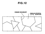
- the crystal domain boundary is formed substantially linear (Fig.
- the dispersion angle in (111) orientation is small, making it possible to obtain an electrode substrate having a dispersion angle of 1° or less.
- the ratio of the maximum diameter of the (111) surface to the height of the planar crystal, i.e., the aspect ratio, of the gold crystal is approximately 30.
- a gold crystal having an aspect ratio of 10 or more can be easily obtained, which is preferably used in the present invention. Under a still more preferable condition, a crystal having an aspect ratio of 100 or more can be obtained.
- the above planar gold substrate can be formed by the following processes: First, I 2 is dissolved in an oxidizing solution having the property to dissolve gold, for example, a KI aqueous solution, in order to obtain an iodine solution in which gold is dissolved to obtain a gold-complex aqueous solution (in which gold is dissolved as a complex having a structure of (AuI 4 ) - ).
- an oxidizing solution having the property to dissolve gold for example, a KI aqueous solution
- an iodine solution in which gold is dissolved to obtain a gold-complex aqueous solution (in which gold is dissolved as a complex having a structure of (AuI 4 ) - ).
- a substrate is immersed in this gold-complex aqueous solution, and, to reduce the insolubility of the gold, the I 2 is removed from the reaction system by evaporating the same by heating or reducing the I 2 to I - by using a reducing agent, and the gold complex is disintegrated by heating or the like to cause it to crystallize on the surface of the substrate.
- the rate of crystallization is high, a grain-cluster-like polycrystal will be generated.
- the planar gold crystal is grown by an oxidizing dissolution reaction while balancing the etching rate with the disintegration rate of the complex. This process suggests a similarity to a vapor-phase epitaxial growth.
- Fig. 4 shows an STM image of a (111) surface grown in the manner described above.
- the STM image of a 1 ⁇ m square i.e., a square area of 1 ⁇ m x 1 ⁇ m
- a substantially flat smooth electrode substrate has been realized in a 1 ⁇ m square area by using the gold crystal.
- the irregularity profile in the Z-axis direction of Fig. 4(b) its surface irregularities consist of atomic-step-like long-period steps of 1nm or less. With this planar gold electrode, it is possible to provide an electrode substrate having a still higher level of smoothness.
- the difference between the highest crest and the deepest recess (the maximum surface irregularity) in a 10 ⁇ m square is 1nm or less and the peak value of irregularity dispersion (the dispersion peak) from the average value of surface irregularity is 0.5nm or less.
- the size of the planar gold crystal under the normal condition ranges from 1 ⁇ m square to 1mm square. Under optimum conditions, it is possible to obtain a crystal having a size of 10mm square or less, that is, several mm square. However, it is also possible for a crystal having a large size of 10mm square or more to be separated, which is controllable, though difficult. Further, it is also possible to prepare an electrode substrate by continuously forming minute planar crystals. Also, with such an electrode substrate it is possible to obtain an electrode substrate in which the (111) plane orientation dispersion angle is smaller than that of a substrate formed by a usual vacuum film formation method, thus making it possible to form an electrode having an excellent orientation property.
- any material can be used for the substrate material as long as it does not cause a serious corrosion in the gold-complex solution.
- the substrate material that can be used include: insulating materials such as mica, MgO, SiO 2 , and Si 3 N 4 ; organic high-molecular weight materials; Si substrates (crystalline or amorphous), which are conductive materials; graphite (HOPG); and various metal substrates and substrates of compounds thereof.
- planar crystal and the production method thereof have been described with reference to the case where gold is adopted as the material, the planar crystal to be grown is not restricted to a gold crystal.
- a similar technique is also applicable to noble metal materials allowing the formation of a complex halide, such as Pt, Pd, Rh, and Ir. Further, it is also applicable to a complex cyanide and a complex sulfite.
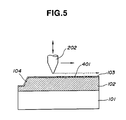
- Fig. 5 is a sectional view of a recording medium using an electrode substrate according to the present invention.
- Numeral 101 indicates a substrate; numeral 102, an electrode layer having a smooth surface; numeral 103, a recording layer; numeral 104, a track; numeral 202, a probe electrode; and numeral 401, a data bit.
- the recording layer may be formed of a material capable of developing a memory-switching phenomenon (an electrical memory effect) having current-voltage characteristics, as for example, an organic monomolecular film or a built-up film thereof, having molecules each including both a group having a ⁇ electron level and a group having a ⁇ electron level deposited only on the electrode. Due to the electrical memory effect, it is possible to reversibly effect transition (switching) between a low-resistance condition (ON condition) and a high-resistance condition (OFF condition) (the ON and OFF conditions in Fig.
- a memory-switching phenomenon an electrical memory effect having current-voltage characteristics
- each of the conditions can be maintained (stored in memory) without applying any voltage.
- organic materials exhibit an insulating or semi-insulating property.
- the organic materials that can be applied to the present invention which contain a group having a ⁇ electron level, include an extremely wide range.
- a dye having a ⁇ electron system which is suitable for the present invention, include: dyes having a porphyrin skeleton, such as phthalocyanine and tetraphenylporphyrin; azulene-type dyes having a squalilium group and a croconic methine group as a bonding chain; dyes similar to a cyanine type or cyanine dyes in which two nitrogen-containing complex rings, such as quinoline, benzothiazole, or benzooxazole, are connected by a squalilium group and a croconic methine group; condensed polycyclic aromatic compounds, such as anthracene and pyrene; chain compounds formed by polymerization of an aromatic cyclic compound or a complex cyclic compound
- a preferable film thickness is in the range of 5 to 300 ⁇ .
- the recording layer 103 is not absolutely necessary. As stated in Phys. Rev. Lett ., 65, 2418 (1990) by H.J. Mamin et al., it is possible to directly cause a perturbation on the surface of the electrode layer 102 so as to selectively generate a disturbance thereon, for example, by depositing fine gold particles on the electrode surface through field evaporation of gold by using a gold probe electrode. According to the above reference, this field evaporation of gold varies somewhat depending upon the distance between the electrode surface and the tip of the probe electrode. With an application voltage of 3.2V or less, the probability that the field evaporation of gold will take place is zero.
- the pulse width which allows recording at this time is 1 ⁇ s or less, making it possible to cope with high-speed recording.
- the pit diameter varies depending upon various conditions. Usually, recording with a pit diameter of 100 to 300 ⁇ is possible, and under more preferable conditions, recording can be effected with a pit diameter of 30 to 100 ⁇ , and further, 30 to 70 ⁇ .
- a grain cluster of 300 to 500 ⁇ is usually generated, so that it is rather difficult to clearly distinguish the recording from the surface irregularities on the electrode substrate. Therefore, in the present invention, use of a smooth electrode substrate according to the present invention is indispensable.
- the direction of the field evaporation largely depends upon the surface condition of the smooth substrate electrode, and the above-described phenomenon occurs regardless of the polarity of the application electrode. That is, by making the polarity on the side of the probe electrode positive, deposition of fine gold particles takes place on the substrate electrode surface, as described above. If, conversely, a positive application is effected on the substrate electrode side, the deposition of gold on the substrate electrode surface takes place in the same way, although the threshold voltage thereof increases. However, it is also possible to position the probe electrode on a minute gold protrusion on the substrate electrode surface and remove the gold protrusion by applying a voltage (erasable).
- Fig. 5 Although methods of directly imparting a perturbation to the electrode layer have been described, it is also possible, as shown in Fig. 5, to provide the recording layer 103 on a smooth electrode surface and selectively cause changes in the conditions of the recording layer, including changes in the configuration thereof, thereby effecting recording.
- the material to be employed for the recording layer it is possible to use an organic compound which allows changes in configuration to take place through irradiation of various types of energy at low levels as described below. Further, by effecting recording through changes in the condition of individual organic molecules, it is possible to obtain a recording density on a molecular scale.
- recording may be effected separately. Generally, however, it is often realized in the form of a combination of a number of effects.
- the formation of the recording layer 103 may be effected by evaporation, the cluster ion beam method or the like.
- the LB method is the most suitable of the conventional methods known in the art. With the LB method, a monomolecular film of an organic compound having in one molecule a hydrophobic portion and a hydrophilic portion, or a built-up film thereof, can be easily formed on a substrate, thereby making it possible to stably provide an organic ultra-thin film which has a thickness of a molecular order and which is uniform and homogeneous over a wide area. Accordingly, it is possible to prepare a recording medium which reflects the surface property of an under-coat electrode substrate as it is.
- a monomolecular film or a built-up film thereof is formed by utilizing the fact that in molecules each having a structure in which hydrophilic and hydrophobic portions exist therein, an appropriate balance is maintained between them, the molecules form a monomolecular layer on a water surface, with the hydrophilic groups facing downwards.
- the group constituting the hydrophobic portion include various types of hydrophobic groups, such as generally well-known saturated and unsaturated hydrocarbon groups, condensed polynuclear aromatic groups, and chain polycyclic phenyl groups. One, or a plurality of types of such groups, are combined to form the hydrophobic portion.
- hydrophilic portion includes various types of hydrophilic groups, such as carboxyl group, ester group, acid amide group, imide group, hydroxyl group, and amino group (of first, second, third or fourth grade).
- hydrophilic groups such as carboxyl group, ester group, acid amide group, imide group, hydroxyl group, and amino group (of first, second, third or fourth grade).
- One, or a plurality of types of such groups, are combined to form the above-mentioned hydrophilic portion.
- the tip of the probe electrode 202 must be as pointed as possible so that the resolution in recording and reproduction may be improved.
- a probe electrode having an atomic resolution can be prepared by an electrolytic polishing method, such as the tungsten method.
- an electrolytic polishing method such as the tungsten method.
- a probe electrode prepared in this way has an atomic resolution.
- the configuration and processing method of the probe electrode are not restricted to those described above.
- Fig. 6 shows the signal frequency spectrum of a signal at point P in the information processing apparatus of the present invention shown in Fig. 7.
- Fig. 7 shows an example of the construction of an information processing apparatus utilizing the principle of the STM, which will be described below with reference to the drawing.
- Numeral 101 indicates a substrate; numeral 102, a metal electrode layer; and numeral 103, a recording layer.
- Numeral 201 indicates an XY stage; numeral 202, a probe electrode; numeral 203, a support member for the probe electrode; numeral 204, a linear actuator for driving the probe electrode 204 in the Z-direction; numerals 205 and 206, linear actuators for driving the XY stage in the X- and Y-directions, respectively; and numeral 207, a pulse voltage circuit.
- Numeral 301 indicates an amplifier for detecting a tunnel current flowing from the probe electrode to the electrode layer 102 by way of the recording layer 103.
- Numeral 302 indicates a logarithmic compressor for converting a change in the tunnel current into a value which is proportional to the gap distance of the recording layer; and
- numeral 303 indicates a low-pass filter for extracting surface irregularity components of the recording layer.
- Numeral 304 indicates an error amplifier for detecting an error between a reference voltage V REF and the low-pass filter 303; and numeral 305 indicates a driver for driving the actuator 204.
- Numeral 306 indicates a drive circuit for performing position control of the XY stage.
- Numeral 307 indicates a high-pass filter for separating data components.
- any signals of a frequency component not higher than f 0 are due to a gentle rise and fall of the substrate 101 due to warp, distortion or the like.
- Symbol f 2 indicates a recording data carrier component
- numeral 403 indicates a data signal band.
- Symbol f 3 indicates a signal component generated from the atomic/molecular arrangement of the recording layer
- symbol f T indicates a tracking signal.
- a signal around f 1 is due to a slight irregularity of the surface of the electrode layer 102, i.e., the (111) surface. This irregularity is made equal to or smaller than the recording signal. In recording and reproduction utilizing the STM, the change in this irregularity approximately corresponds to five layers of electrode materials (1nm or less).
- the size of the smooth surface of the surface of the recording layer 103 is 1 ⁇ m square. Under a more favorable condition, 10 ⁇ m or more. This provides the following advantages:
- An iodine solution was prepared by dissolving 4g of potassium iodide (KI) and 0.6g of iodine (I 2 ) in 50ml of pure water. Then, a 5000 ⁇ thick gold film formed by vacuum evaporation (approximately 0.08g in terms of weight) was completely dissolved in the iodine solution to obtain a gold/iodine-complex stock solution. 10ml of this stock solution was pipetted and diluted in 50ml of pure water to prepare a reaction mother liquor. A silicon substrate whose natural oxide film had been etched by hydrofluoric acid was immersed in the mother liquor and heated to 80°C on a hot plate.
- KI potassium iodide
- I 2 iodine
- a track 104 having a width of 0.1 ⁇ m, a pitch of 1.0 ⁇ m, and a depth of 50 ⁇ was formed on the surface of the flat gold crystal electrode by a focused ion beam.
- the focused ion beam process was conducted by using gold ions under the following conditions: acceleration voltage: 40KV; ion current: 14pA; dose amount: 1.0 x 10 16 /cm 2 .
- a four-layered polyimide LB film was formed on the smooth electrode substrate, prepared in the above-described manner, as the recording layer 103.
- the recording layer 103 was formed by using the polyimide LB film as follows.
- a polyamide acid as shown in formula (1) was dissolved in an N,N'-dimethylacetamide/benzene mixture solution of 1:1 (V/V) (density in terms of monomer: 1 x 10 -3 M). Then, it was mixed with a separately prepared 1 x 10 -3 M solution of N,N'-dimethyloctadecylamine in the same solvent in a proportion of 1:2 (V/V) to prepare a polyamide-acid-octadecylamine salt solution as shown in formula (2).
- This solution was developed on a water phase consisting of pure water at a temperature of 20°C to form a monomolecular film on the surface of the water.
- the surface pressure was augmented to 25 mN/m.
- the above substrate electrode was gently immersed in such a way as to traverse the water surface at a rate of 5 mm/min, and was then pulled up gently at a rate of 5 mm/min to prepare a two-layered Y-type monomolecular built-up film. By repeating this operation, a four-layered monomolecular built-up film of polyamide-acid-octadecylamine salt was formed.
- this substrate was calcinated by heating for thirty minutes at 200°C under a reduced pressure ( ⁇ 1 mmHg) to imidize the polyamide-acid-octadecylamine salt (Formula 3), thereby obtaining a four-layered polyimide monomolecular built-up film.
- the surface configuration of a recording medium prepared in the above-described manner was examined on the information processing apparatus shown in Fig. 7. Upon examination, it was found that the surface of the recording medium reflected the smoothness of the electrode and the track 104. In a 10 ⁇ m square, the track 104 had been formed to a depth of 50 ⁇ , and, outside the track 104, the maximum surface irregularity was 0.9nm, with the dispersion peak being 0.4nm. Accordingly, the track 104 could be clearly distinguished.
- a platinum/rhodium probe electrode 202 was used as the probe electrode 202.
- the probe electrode 202 is used for the purpose of controlling the distance (Z) between it and the recording layer 103, and is under a fine current control to a constant level.
- the linear actuators 204, 205 and 206 are designed such that they allow fine control also in the in-plane (X, Y) directions while keeping the distance Z constant.
- the probe electrode 202 is capable of directly effecting recording, reproduction and erasing. Additionally, the recording medium is placed on the high-precision XY stage 201 and can be moved to an arbitrary position.
- the recording layer 103 comprising a four-layered polyimide film as described above, was placed on the XY stage 201. Then, a voltage of +1.5V was applied between the probe electrode 202 and the electrode layer 102 of the recording medium, and the distance (Z) between the probe electrode 202 and the surface of the recording layer 103 was adjusted while monitoring the current. At this time, a probe current Ip for controlling the distance Z between the probe electrode 202 and the surface of the recording medium was set in such a way that 10 -10 A ⁇ Ip ⁇ 10 -11 A.
- the probe electrode 202 was positioned on the + side and the electrode layer 102 on the - side, applying a rectangular pulse voltage beyond a threshold voltage V th ON causing the electric memory material (the four-layered polyimide film) to be changed to a low-resistance condition (ON condition). Afterwards, the probe electrode 202 was brought back to the recording start point, and was caused to scan the recording layer 103 again. Here, adjustment was made in such a way that Z was constant at the time of reading of the recorded information. As a result, it was shown that in the recording bit, a probe current of approximately 10nA flowed, under the ON condition.
- the probe voltage was set at 10V which is above the threshold voltage V th OFF causing the electric memory material to change from the ON to the OFF condition.
- the recording position was traced again to confirm that this caused the entire recording conditions to be erased, thereby causing the material to be changed to the OFF condition.
- a recording pulse was applied in accordance with the above recording method to a position which was in the OFF condition with the recording condition erased to confirm that it caused the material to be changed to the OFF condition. It was also confirmed that the recording condition could be erased again.
- Example 1 shows the surface properties of the electrode layers used in the experiment.
- Substrate type Dispersion angle Surface irregularity (in 10 ⁇ m square) Maximum surface irregularity Dispersion peak Si (etched) 0.9° 0.8nm 0.4nm HOPG 0.6° 0.7nm 0.3nm Au/Si 0.9° 0.8nm 0.4nm Cr/Si 0.9° 0.8nm 0.4nm Al/Si 0.9° 0.9nm 0.4nm a-Si/SiO 2 (thermal oxidation film) 0.9° 0.9nm 0.4nm Glass 1.0° 1.0nm 0.4nm SiO 2 /Si (thermal oxidation film) 0.9° 0.8nm 0.4nm SiN/Si 1.0° 0.9nm 0.4nm MgO 0.6° 1.0nm 0.4nm Polyimide (capton)
- Example 1 A planar gold crystal like that of Example 1 was formed under the same experimental conditions as in Example 1 except that instead of taking the iodine out of the reaction system by sublimation, the iodine was reduced by using reducing agents.
- the reducing agents used in the experiment were sulfite ions and hydroquinone.
- the substrate was a silicon substrate and the crystallization temperature was 60°C.
- Example 2 An experiment was conducted in which the gold concentration of the stock solution of Example 1 and the crystallization temperature were varied. The results are summarized in Table 2.
- the substrate used was a silicon crystal substrate.
- a silicon substrate and a glass (SiO 2 ) substrate which had been surface-processed by various well-known methods in such a manner that the matrix intersections at intervals of 500 ⁇ m were made 1 ⁇ m to 2 ⁇ m square were immersed in the mother liquor used in Example 1 to observe how crystallization took place under the same conditions as in Example 1.
- Each of the seed substrates for selective deposition used in the experiment was prepared in the following manner:
- Example 2 four layers of polyimide monomolecular films were accumulated on an electrode substrate prepared by the method 5 ⁇ to form a recording medium, which was examined for surface configuration on the information processing apparatus shown in Fig. 7.
- the surface of the recording medium reflected the smoothness of the electrode, and the maximum surface irregularity in a 10 ⁇ m square was 0.9nm or less, with the dispersion peak being 0.4nm or less.
- the planar gold crystal selectively deposited formed a (111) plane orientation facet, which was in the same pattern as the seed pattern used. Further, the edges of the facet reflected the characteristics of the crystal surface so as to provide a track of a very high degree of linearity (see Fig. 12). The track groove formed was deep, so that the track could be clearly distinguished as in Example 1.
- Example 1 An experiment was performed on recording, reproduction and erasing, and it was confirmed that recording, reproduction and erasing could be performed as in Example 1 with an electrode substrate prepared in the above-described manner. Further, it was also confirmed that recording, reproduction and erasing could be performed with electrode substrates prepared by other methods as described above.
- Example 6 a selective deposition of gold as shown in Example 6 is also possible with a combination of the selective deposition according to the method of Example 5 and the crystal growth process shown in Example 1.
- a track 104 having a width of 0.1 ⁇ m, a pitch of 1.0 ⁇ m and a depth of 5.0 ⁇ was formed on the surface of the planar gold crystal electrode by a focused ion beam, using gold ions under the following conditions: acceleration voltage: 40KV; ion current: 14pA; and dose amount: 1.0 x 10 16 /cm 2 .
- a gold wire having a diameter of 250 ⁇ m was formed into a gold chip through electrolytic polishing in concentrated hydrochloric acid (1.5 to 2 Vdc), thereby preparing a gold probe electrode 202, which was used in an experiment on recording and reproduction.
- the probe electrode 202 is intended for the control of the distance (Z) between it and the recording layer 103, and is under a fine current control to attain a constant level. Further, the linear actuators 204, 205 and 206 are so designed as to allow fine motion control in the in-plane directions (X, Y) while maintaining the distance Z constant.
- the probe electrode 202 is capable of directly performing recording, reproduction and erasing. Moreover, the recording medium is placed on the high-precision XY stage 201 and can be moved to an arbitrary position.
- the above-mentioned gold substrate electrode was placed on the XY stage 201. Then, a voltage of +1.5V was applied between the probe electrode 202 and the gold substrate electrode 102, and the distance (Z) between the probe electrode 202 and the recording medium 103 was adjusted while monitoring the current.
- a setting was made in such a manner that the probe current Ip for controlling the distance Z between the probe electrode 202 and the surface of the recording medium 103 was kept in the range: 10 -10 A ⁇ Ip ⁇ 10 -11 A.
- a gold substrate electrode was formed in the same manner as in Example 7.
- a two-layered spiropyran LB film was formed on the prepared gold substrate electrode, thereby preparing the recording layer 103.
- a description will be given on how the recording layer 103 using the spiropyran LB film was formed.
- a mixture solution of a spiropyran derivative with an octadecyl group introduced therein and arachidic acid in the proportion of 1 : 2 (solvent: chloroform in a concentration of 1 x 10 -3 M) was developed on a water phase consisting of an aqueous solution of CdCl 2 (concentration: 1 x 10 -4 M) at a temperature of 20°C to form a monomolecular film on the water surface.
- the surface pressure was raised up to 30 mN/m. While keeping the surface pressure constant, the above substrate electrode was gently immersed in such a way as to traverse the water surface at a rate of 5 mm/min. Then, it was gently pulled up, thereby forming a two-layered Y-type monomolecular built-up film.
- Example 7 Using the mother liquor described in Example 7, electrode layers were formed on various types of substrates, and an experiment similar to that of Example 7 was conducted. The surface properties of the electrode layers used in the experiment are summarized in Table 1 (shown above).
- Example 7 the surface of each recording medium reflected the smoothness of the electrode and the track 104.
- the track 104 had been formed 50 ⁇ deep, and the maximum surface irregularity outside the track 104 was 0.9nm or less, with the dispersion peak being 0.4nm or less. Therefore, as in Example 7, the track 104 could be clearly distinguished.
- an experiment was conducted on recording, reproduction and erasing. It was confirmed that recording, reproduction and erasing could be performed as in Example 7.
- Example 7 Further, a recording/reproduction experiment similar to that of Example 7 was performed using a spiropyran LB film as the recording layer, as in Example 8, and it was confirmed that recording and reproduction could be performed as in Example 7. Also, the average bit diameter was substantially the same value.
- a silicon substrate and a glass (SiO 2 ) substrate which had been surface-processed by various well-known methods in such a way as to make the matrix intersections at intervals of 500 ⁇ m 1 ⁇ m to 2 ⁇ m square were immersed in the mother liquor used in Example 7 to observe how crystallization occurred under the same conditions as in Example 7.
- Each of the seed substrates for selective deposition used in the experiment was prepared in the following manner:
- an electrode substrate prepared by the method 5 ⁇ was examined for surface configuration on the information processing apparatus shown in Fig. 7.
- the maximum surface irregularity in a 10 ⁇ m square was 0.9nm or less, with the dispersion peak being 0.4nm or less.
- Example 7 An experiment was performed on recording, reproduction and erasing, and it was confirmed that recording, reproduction and erasing could be performed as in Example 7. Further, it was also confirmed that recording, reproduction and erasing could be performed with electrode substrates prepared by other methods as described above.
- the present invention provides the following advantages:
Landscapes
- Chemical & Material Sciences (AREA)
- Engineering & Computer Science (AREA)
- Crystallography & Structural Chemistry (AREA)
- Materials Engineering (AREA)
- Metallurgy (AREA)
- Organic Chemistry (AREA)
- Nanotechnology (AREA)
- Mathematical Physics (AREA)
- Theoretical Computer Science (AREA)
- Physics & Mathematics (AREA)
- Semiconductor Memories (AREA)
- Analysing Materials By The Use Of Radiation (AREA)
- Electrical Discharge Machining, Electrochemical Machining, And Combined Machining (AREA)
- Measurement And Recording Of Electrical Phenomena And Electrical Characteristics Of The Living Body (AREA)
- Investigating Or Analyzing Materials By The Use Of Electric Means (AREA)
Claims (23)
- Substrat-électrode comprenant un substrat (101) et une couche servant d'électrode (102) constituée d'un métal noble formée sur ledit substrat (101), caractérisé en ce que la surface de ladite couche servant d'électrode (102) est formée par une facette d'orientation dans le plan (111) d'un monocristal, et en ce que les limites de domaines des faces cristallines dudit monocristal sont essentiellement linéaires.
- Substrat-électrode suivant la revendication 1, dans lequel la surface de la couche servant d'électrode (102) présente un angle de dispersion d'orientation dans le plan, mesuré par analyse aux rayons X, égal ou inférieur à 1°.
- Substrat-électrode suivant la revendication 1, dans lequel le cristal de métal noble a un rapport d'allongement égal ou supérieur à 10.
- Substrat-électrode suivant la revendication 1, dans lequel le substrat (101) comprend un substrat conducteur et une couche isolante formée sur le substrat conducteur.
- Substrat-électrode suivant la revendication 4, dans lequel la couche isolante comporte un trou de passage, le cristal de métal noble (102) étant formé par croissance cristalline à partir du substrat conducteur à travers ledit trou de passage.
- Substrat-électrode suivant la revendication 2, dans lequel l'angle de dispersion d'orientation dans le plan est égal ou inférieur à 0,6°.
- Substrat-électrode suivant la revendication 1, dans lequel l'irrégularité maximale de surface dans une zone dans le plan de 1 µm x 1 µm de la couche servant d'électrode (102) est égale ou inférieure à 1 nm.
- Support d'enregistrement d'informations comprenant un substrat-électrode (101, 102) suivant l'une quelconque des revendications 1 à 7 comme couche d'enregistrement.
- Support d'enregistrement d'informations comprenant une couche d'enregistrement (103) sur un substrat-électrode (101, 102) suivant l'une quelconque des revendications 1 à 7.
- Support d'enregistrement d'informations suivant la revendication 9, dans lequel la couche d'enregistrement (103) consiste en un film monomoléculaire d'un composé organique ou un film formé par accumulation d'un tel film monomoléculaire.
- Support d'enregistrement d'informations suivant la revendication 9, dans lequel la couche d'enregistrement (103) a une épaisseur comprise dans l'intervalle de 5 à 300 Å.
- Support d'enregistrement d'informations suivant la revendication 9, dans lequel la couche d'enregistrement (103) permet un enregistrement d'informations sous forme de variations de conditions physiques.
- Support d'enregistrement d'informations suivant la revendication 9, dans lequel la couche d'enregistrement (103) a un effet de mémoire.
- Support d'enregistrement d'informations suivant l'une des revendications 8 et 9, comprenant en outre une piste (104).
- Appareil comprenant :un support d'enregistrement d'informations (101-104) suivant l'une quelconque des revendications 8 à 14 ;une électrode-sonde (202) placée à proximité immédiate du support (101-104) ; etun circuit d'application de tension (207) pour l'application d'une tension impulsionnelle entre ledit support (101-104) et ladite électrode-sonde (202), de manière à permettre l'écriture d'une information sur ledit support.
- Appareil comprenant :un support d'enregistrement d'informations (101-104) suivant l'une des revendications 8 à 14 ;une électrode-sonde (202) placée à proximité immédiate du support (101-104) ;un premier circuit d'application de tension (207) pour l'application d'une tension impulsionnelle entre ledit support (101-104) et ladite électrode-sonde (202), etun second circuit d'application de tension pour l'application d'une tension de polarisation entre ledit support (101-104) et ladite électrode-sonde (202), l'information étant écrite sur ledit support (101-104) par application de ladite tension impulsionnelle et par lecture à partir dudit support (101-104) par application de ladite tension de polarisation.
- Appareil comprenant :un support d'enregistrement d'informations (101-104) suivant une des revendications 8 à 14 ;une électrode-sonde (202) placée à proximité immédiate de ce support ; etun circuit d'application de tension pour l'application d'une tension de polarisation entre ledit support et ladite électrode-sonde (202), de manière à permettre la lecture d'une information à partir dudit support.
- Appareil suivant l'une des revendication 15 à 17, dans lequel une pluralité des électrodes-sondes (202) est présente.
- Appareil suivant une des revendications 15 et 16, dans lequel une perturbation est transmise à la surface du support (101-104) par application de la tension impulsionnelle de manière à engendrer sélectivement une perturbation.
- Procédé de traitement d'informations, comprenant les étapes consistant :à préparer un support d'enregistrement d'informations (101-104) suivant une des revendications 8 à 14 ;à placer une électrode-sonde (202) à proximité immédiate dudit support (101-104) ; età appliquer une tension impulsionnelle entre ledit support (101-104) et ladite électrode-sonde (202) de manière à permettre l'écriture d'une information sur ledit support (101-104).
- Procédé de traitement d'informations, comprenant les étapes consistant :à préparer un support d'enregistrement d'informations (101-104) suivant l'une des revendications 8 à 14 ;à placer une électrode-sonde (202) à proximité immédiate dudit support (101-104) ;à appliquer une tension impulsionnelle entre ledit support (101-104) et ladite électrode-sonde (202) de manière à permettre l'écriture d'une information sur ledit support (101-104) ;à appliquer une tension de polarisation entre ledit support (101-104) et ladite électrode-sonde (202) de manière à permettre la lecture de l'information à partir dudit support.
- Procédé de traitement d'informations, comprenant les étapes consistant :à préparer un support d'enregistrement d'informations (101-104) suivant l'une des revendications 8 à 14, sur lequel une information (401) a été enregistrée préalablement ;à placer une électrode-sonde (202) à proximité immédiate dudit support (101-104) ; età appliquer une tension de polarisation entre ledit support et ladite électrode-sonde (202) de manière à permettre la lecture de l'information (401) à partir dudit support.
- Procédé de traitement d'informations suivant l'une des revendications 20 et 21, dans lequel, par application de la tension impulsionnelle, une perturbation est transmise à la surface du support (101-104) de manière à engendrer sélectivement une perturbation.
Applications Claiming Priority (4)
| Application Number | Priority Date | Filing Date | Title |
|---|---|---|---|
| JP213054/91 | 1991-07-31 | ||
| JP21305491 | 1991-07-31 | ||
| JP21305591 | 1991-07-31 | ||
| JP213055/91 | 1991-07-31 |
Publications (2)
| Publication Number | Publication Date |
|---|---|
| EP0526237A1 EP0526237A1 (fr) | 1993-02-03 |
| EP0526237B1 true EP0526237B1 (fr) | 1998-04-08 |
Family
ID=26519591
Family Applications (1)
| Application Number | Title | Priority Date | Filing Date |
|---|---|---|---|
| EP92307006A Expired - Lifetime EP0526237B1 (fr) | 1991-07-31 | 1992-07-30 | Appareil de traitement de l'information et substrat d'électrode et milieu de réception de l'information appliquer à l'appareil |
Country Status (6)
| Country | Link |
|---|---|
| US (1) | US5329514A (fr) |
| EP (1) | EP0526237B1 (fr) |
| JP (1) | JP2981804B2 (fr) |
| AT (1) | ATE164963T1 (fr) |
| CA (1) | CA2074914C (fr) |
| DE (1) | DE69225032T2 (fr) |
Families Citing this family (25)
| Publication number | Priority date | Publication date | Assignee | Title |
|---|---|---|---|---|
| JPH06187675A (ja) * | 1992-09-25 | 1994-07-08 | Canon Inc | 情報処理装置、及びそれを用いる情報処理方法 |
| US5495109A (en) * | 1995-02-10 | 1996-02-27 | Molecular Imaging Corporation | Electrochemical identification of molecules in a scanning probe microscope |
| JPH09293283A (ja) * | 1996-04-25 | 1997-11-11 | Hewlett Packard Co <Hp> | プローブ装置およびその製造方法、ならびにメディア移動型メモリ装置 |
| JPH10188375A (ja) * | 1996-12-17 | 1998-07-21 | Canon Inc | 記録媒体 |
| US7260051B1 (en) | 1998-12-18 | 2007-08-21 | Nanochip, Inc. | Molecular memory medium and molecular memory integrated circuit |
| US6500510B1 (en) | 1999-11-04 | 2002-12-31 | Molecular Storage Technologies, Inc. | Molecular level optical information storage devices |
| US7235092B2 (en) * | 1999-11-19 | 2007-06-26 | Advanced Bio Prosthetic Surfaces, Ltd. | Guidewires and thin film catheter-sheaths and method of making same |
| US10172730B2 (en) * | 1999-11-19 | 2019-01-08 | Vactronix Scientific, Llc | Stents with metallic covers and methods of making same |
| US6379383B1 (en) | 1999-11-19 | 2002-04-30 | Advanced Bio Prosthetic Surfaces, Ltd. | Endoluminal device exhibiting improved endothelialization and method of manufacture thereof |
| US7195641B2 (en) | 1999-11-19 | 2007-03-27 | Advanced Bio Prosthetic Surfaces, Ltd. | Valvular prostheses having metal or pseudometallic construction and methods of manufacture |
| US6849085B2 (en) | 1999-11-19 | 2005-02-01 | Advanced Bio Prosthetic Surfaces, Ltd. | Self-supporting laminated films, structural materials and medical devices manufactured therefrom and method of making same |
| US7736687B2 (en) * | 2006-01-31 | 2010-06-15 | Advance Bio Prosthetic Surfaces, Ltd. | Methods of making medical devices |
| US6537310B1 (en) | 1999-11-19 | 2003-03-25 | Advanced Bio Prosthetic Surfaces, Ltd. | Endoluminal implantable devices and method of making same |
| US8458879B2 (en) * | 2001-07-03 | 2013-06-11 | Advanced Bio Prosthetic Surfaces, Ltd., A Wholly Owned Subsidiary Of Palmaz Scientific, Inc. | Method of fabricating an implantable medical device |
| JP2005503178A (ja) * | 2000-01-25 | 2005-02-03 | ボストン サイエンティフィック リミテッド | 蒸着による医療器具の製造 |
| US6695865B2 (en) | 2000-03-20 | 2004-02-24 | Advanced Bio Prosthetic Surfaces, Ltd. | Embolic protection device |
| US9566148B2 (en) | 2000-05-12 | 2017-02-14 | Vactronix Scientific, Inc. | Self-supporting laminated films, structural materials and medical devices manufactured therefrom and methods of making same |
| US7233517B2 (en) | 2002-10-15 | 2007-06-19 | Nanochip, Inc. | Atomic probes and media for high density data storage |
| AT500259B1 (de) * | 2003-09-09 | 2007-08-15 | Austria Tech & System Tech | Dünnschichtanordnung und verfahren zum herstellen einer solchen dünnschichtanordnung |
| US7420106B2 (en) * | 2005-03-18 | 2008-09-02 | The University Of Utah Research Foundation | Scanning probe characterization of surfaces |
| US7367119B2 (en) | 2005-06-24 | 2008-05-06 | Nanochip, Inc. | Method for forming a reinforced tip for a probe storage device |
| US7463573B2 (en) | 2005-06-24 | 2008-12-09 | Nanochip, Inc. | Patterned media for a high density data storage device |
| US20070041237A1 (en) * | 2005-07-08 | 2007-02-22 | Nanochip, Inc. | Media for writing highly resolved domains |
| US7309630B2 (en) | 2005-07-08 | 2007-12-18 | Nanochip, Inc. | Method for forming patterned media for a high density data storage device |
| US20070195682A1 (en) * | 2006-02-21 | 2007-08-23 | Duerig Urs T | Method for high density data storage and imaging |
Citations (3)
| Publication number | Priority date | Publication date | Assignee | Title |
|---|---|---|---|---|
| US4896044A (en) * | 1989-02-17 | 1990-01-23 | Purdue Research Foundation | Scanning tunneling microscope nanoetching method |
| EP0412829A2 (fr) * | 1989-08-10 | 1991-02-13 | Canon Kabushiki Kaisha | Milieu d'enregistrement, méthode pour la fabrication de ceci, dispositif d'enregistrement et de réproduction et méthode d'enregistrement, réproduction et d'effacement utilisant un tel milieu |
| EP0441626A2 (fr) * | 1990-02-07 | 1991-08-14 | Canon Kabushiki Kaisha | Milieu, procédé pour le préparer, dispositif de traitement d'information et méthode de traitement d'information |
Family Cites Families (7)
| Publication number | Priority date | Publication date | Assignee | Title |
|---|---|---|---|---|
| US4575822A (en) * | 1983-02-15 | 1986-03-11 | The Board Of Trustees Of The Leland Stanford Junior University | Method and means for data storage using tunnel current data readout |
| JPS6180536A (ja) * | 1984-09-14 | 1986-04-24 | ゼロツクス コーポレーシヨン | 原子規模密度情報記緑および読出し装置並びに方法 |
| JP2556491B2 (ja) * | 1986-12-24 | 1996-11-20 | キヤノン株式会社 | 記録装置及び記録法 |
| JP2556492B2 (ja) * | 1986-12-24 | 1996-11-20 | キヤノン株式会社 | 再生装置及び再生法 |
| DE3701412A1 (de) * | 1987-01-20 | 1988-07-28 | Bayer Ag | Verfahren zum ein- bzw. auslesen von informationen in elektrisch polarisierbare schichten unter verwendung eines rastertunnelmikroskops |
| US4868396A (en) * | 1987-10-13 | 1989-09-19 | Arizona Board Of Regents, Arizona State University | Cell and substrate for electrochemical STM studies |
| JPH02295050A (ja) * | 1989-05-09 | 1990-12-05 | Olympus Optical Co Ltd | μ―STMを用いた回路パターン作製装置および回路パターン作製方法 |
-
1992
- 1992-07-02 JP JP4197454A patent/JP2981804B2/ja not_active Expired - Fee Related
- 1992-07-27 US US07/919,273 patent/US5329514A/en not_active Expired - Lifetime
- 1992-07-29 CA CA002074914A patent/CA2074914C/fr not_active Expired - Fee Related
- 1992-07-30 AT AT92307006T patent/ATE164963T1/de not_active IP Right Cessation
- 1992-07-30 EP EP92307006A patent/EP0526237B1/fr not_active Expired - Lifetime
- 1992-07-30 DE DE69225032T patent/DE69225032T2/de not_active Expired - Fee Related
Patent Citations (3)
| Publication number | Priority date | Publication date | Assignee | Title |
|---|---|---|---|---|
| US4896044A (en) * | 1989-02-17 | 1990-01-23 | Purdue Research Foundation | Scanning tunneling microscope nanoetching method |
| EP0412829A2 (fr) * | 1989-08-10 | 1991-02-13 | Canon Kabushiki Kaisha | Milieu d'enregistrement, méthode pour la fabrication de ceci, dispositif d'enregistrement et de réproduction et méthode d'enregistrement, réproduction et d'effacement utilisant un tel milieu |
| EP0441626A2 (fr) * | 1990-02-07 | 1991-08-14 | Canon Kabushiki Kaisha | Milieu, procédé pour le préparer, dispositif de traitement d'information et méthode de traitement d'information |
Non-Patent Citations (1)
| Title |
|---|
| 'Grundlagen der Festkörperphysik', Weissmantel, Hamann, VEB Verlag, Berlin 1981, pages 614-615 * |
Also Published As
| Publication number | Publication date |
|---|---|
| US5329514A (en) | 1994-07-12 |
| EP0526237A1 (fr) | 1993-02-03 |
| CA2074914C (fr) | 1997-12-02 |
| DE69225032T2 (de) | 1998-08-13 |
| JP2981804B2 (ja) | 1999-11-22 |
| ATE164963T1 (de) | 1998-04-15 |
| JPH05303774A (ja) | 1993-11-16 |
| CA2074914A1 (fr) | 1993-02-01 |
| DE69225032D1 (de) | 1998-05-14 |
Similar Documents
| Publication | Publication Date | Title |
|---|---|---|
| US5329514A (en) | Information processing apparatus, and electrode substrate and information recording medium used in the apparatus | |
| EP0551966B1 (fr) | Appareil d'enregistrement et appareil de reproduction | |
| US5481528A (en) | Information processor and method using the information processor | |
| JP2884447B2 (ja) | カンチレバー型プローブ、及びこれを用いた走査型トンネル顕微鏡、情報処理装置 | |
| EP0519745B1 (fr) | Milieu d'enregistrement, appareil de traitement d'information l'utilisant et méthode d'effacement d'information | |
| EP0416920B1 (fr) | Procédé et dispositif de traitement d'information | |
| US5812516A (en) | Maintaining interatomic distance between an STM probe and a recording layer | |
| JPH03156749A (ja) | 記録媒体用基板及びその製造方法、記録媒体、記録方法、記録再生方法、記録装置、記録再生装置 | |
| JP3135779B2 (ja) | 情報処理装置 | |
| EP0553937B1 (fr) | Appareil d'enregistrement et appareil de reproduction | |
| JP2783646B2 (ja) | 情報記録再生装置 | |
| JP2942013B2 (ja) | 記録及び/又は再生装置 | |
| JP2603270B2 (ja) | 記録装置および再生装置 | |
| JPH06264217A (ja) | プローブ及びそれを用いた走査型プローブ顕微鏡並びに情報処理装置 | |
| JP2556520B2 (ja) | 記録装置及び記録法 | |
| EP0449409A2 (fr) | Sonde, appareil de traitement d'information utilisant la sonde, et méthodes d'utilisation et fabrication | |
| JP2981789B2 (ja) | 記録媒体及び情報処理装置 | |
| JP3005077B2 (ja) | 記録及び/又は再生方法及び装置 | |
| JP3060143B2 (ja) | 記録媒体及びそれを用いた情報処理装置 | |
| JP2862352B2 (ja) | 情報処理方法及び情報処理装置 | |
| JP3261539B2 (ja) | 電極基板の製造方法 | |
| JPH06333276A (ja) | 記録媒体及びその製造方法、及び該記録媒体を用いた情報処理装置 | |
| JP2992908B2 (ja) | 基板電極の製造方法、記録媒体の製造方法 | |
| JP3220914B2 (ja) | 記録媒体製造方法 | |
| JPH05234156A (ja) | プローブ構造体、記録装置、情報検出装置、再生装置及び記録再生装置 |
Legal Events
| Date | Code | Title | Description |
|---|---|---|---|
| PUAI | Public reference made under article 153(3) epc to a published international application that has entered the european phase |
Free format text: ORIGINAL CODE: 0009012 |
|
| AK | Designated contracting states |
Kind code of ref document: A1 Designated state(s): AT BE CH DE DK ES FR GB GR IT LI LU NL PT SE |
|
| 17P | Request for examination filed |
Effective date: 19930618 |
|
| 17Q | First examination report despatched |
Effective date: 19960410 |
|
| GRAG | Despatch of communication of intention to grant |
Free format text: ORIGINAL CODE: EPIDOS AGRA |
|
| GRAG | Despatch of communication of intention to grant |
Free format text: ORIGINAL CODE: EPIDOS AGRA |
|
| GRAH | Despatch of communication of intention to grant a patent |
Free format text: ORIGINAL CODE: EPIDOS IGRA |
|
| GRAH | Despatch of communication of intention to grant a patent |
Free format text: ORIGINAL CODE: EPIDOS IGRA |
|
| GRAA | (expected) grant |
Free format text: ORIGINAL CODE: 0009210 |
|
| AK | Designated contracting states |
Kind code of ref document: B1 Designated state(s): AT BE CH DE DK ES FR GB GR IT LI LU NL PT SE |
|
| ITF | It: translation for a ep patent filed | ||
| PG25 | Lapsed in a contracting state [announced via postgrant information from national office to epo] |
Ref country code: NL Free format text: LAPSE BECAUSE OF FAILURE TO SUBMIT A TRANSLATION OF THE DESCRIPTION OR TO PAY THE FEE WITHIN THE PRESCRIBED TIME-LIMIT Effective date: 19980408 Ref country code: LI Free format text: LAPSE BECAUSE OF FAILURE TO SUBMIT A TRANSLATION OF THE DESCRIPTION OR TO PAY THE FEE WITHIN THE PRESCRIBED TIME-LIMIT Effective date: 19980408 Ref country code: GR Free format text: LAPSE BECAUSE OF FAILURE TO SUBMIT A TRANSLATION OF THE DESCRIPTION OR TO PAY THE FEE WITHIN THE PRESCRIBED TIME-LIMIT Effective date: 19980408 Ref country code: ES Free format text: THE PATENT HAS BEEN ANNULLED BY A DECISION OF A NATIONAL AUTHORITY Effective date: 19980408 Ref country code: CH Free format text: LAPSE BECAUSE OF FAILURE TO SUBMIT A TRANSLATION OF THE DESCRIPTION OR TO PAY THE FEE WITHIN THE PRESCRIBED TIME-LIMIT Effective date: 19980408 Ref country code: BE Free format text: LAPSE BECAUSE OF FAILURE TO SUBMIT A TRANSLATION OF THE DESCRIPTION OR TO PAY THE FEE WITHIN THE PRESCRIBED TIME-LIMIT Effective date: 19980408 Ref country code: AT Free format text: LAPSE BECAUSE OF FAILURE TO SUBMIT A TRANSLATION OF THE DESCRIPTION OR TO PAY THE FEE WITHIN THE PRESCRIBED TIME-LIMIT Effective date: 19980408 |
|
| REF | Corresponds to: |
Ref document number: 164963 Country of ref document: AT Date of ref document: 19980415 Kind code of ref document: T |
|
| REG | Reference to a national code |
Ref country code: CH Ref legal event code: EP |
|
| REF | Corresponds to: |
Ref document number: 69225032 Country of ref document: DE Date of ref document: 19980514 |
|
| PG25 | Lapsed in a contracting state [announced via postgrant information from national office to epo] |
Ref country code: SE Free format text: LAPSE BECAUSE OF FAILURE TO SUBMIT A TRANSLATION OF THE DESCRIPTION OR TO PAY THE FEE WITHIN THE PRESCRIBED TIME-LIMIT Effective date: 19980708 Ref country code: PT Free format text: LAPSE BECAUSE OF FAILURE TO SUBMIT A TRANSLATION OF THE DESCRIPTION OR TO PAY THE FEE WITHIN THE PRESCRIBED TIME-LIMIT Effective date: 19980708 Ref country code: DK Free format text: LAPSE BECAUSE OF FAILURE TO SUBMIT A TRANSLATION OF THE DESCRIPTION OR TO PAY THE FEE WITHIN THE PRESCRIBED TIME-LIMIT Effective date: 19980708 |
|
| PG25 | Lapsed in a contracting state [announced via postgrant information from national office to epo] |
Ref country code: LU Free format text: LAPSE BECAUSE OF NON-PAYMENT OF DUE FEES Effective date: 19980730 |
|
| ET | Fr: translation filed | ||
| NLV1 | Nl: lapsed or annulled due to failure to fulfill the requirements of art. 29p and 29m of the patents act | ||
| REG | Reference to a national code |
Ref country code: CH Ref legal event code: PL |
|
| PLBE | No opposition filed within time limit |
Free format text: ORIGINAL CODE: 0009261 |
|
| STAA | Information on the status of an ep patent application or granted ep patent |
Free format text: STATUS: NO OPPOSITION FILED WITHIN TIME LIMIT |
|
| 26N | No opposition filed | ||
| REG | Reference to a national code |
Ref country code: GB Ref legal event code: IF02 |
|
| PGFP | Annual fee paid to national office [announced via postgrant information from national office to epo] |
Ref country code: DE Payment date: 20040922 Year of fee payment: 13 |
|
| PGFP | Annual fee paid to national office [announced via postgrant information from national office to epo] |
Ref country code: GB Payment date: 20050718 Year of fee payment: 14 |
|
| PGFP | Annual fee paid to national office [announced via postgrant information from national office to epo] |
Ref country code: FR Payment date: 20050719 Year of fee payment: 14 |
|
| PG25 | Lapsed in a contracting state [announced via postgrant information from national office to epo] |
Ref country code: DE Free format text: LAPSE BECAUSE OF NON-PAYMENT OF DUE FEES Effective date: 20060201 |
|
| PG25 | Lapsed in a contracting state [announced via postgrant information from national office to epo] |
Ref country code: GB Free format text: LAPSE BECAUSE OF NON-PAYMENT OF DUE FEES Effective date: 20060730 |
|
| PGFP | Annual fee paid to national office [announced via postgrant information from national office to epo] |
Ref country code: IT Payment date: 20060731 Year of fee payment: 15 |
|
| GBPC | Gb: european patent ceased through non-payment of renewal fee |
Effective date: 20060730 |
|
| REG | Reference to a national code |
Ref country code: FR Ref legal event code: ST Effective date: 20070330 |
|
| PG25 | Lapsed in a contracting state [announced via postgrant information from national office to epo] |
Ref country code: FR Free format text: LAPSE BECAUSE OF NON-PAYMENT OF DUE FEES Effective date: 20060731 |
|
| PG25 | Lapsed in a contracting state [announced via postgrant information from national office to epo] |
Ref country code: IT Free format text: LAPSE BECAUSE OF NON-PAYMENT OF DUE FEES Effective date: 20070730 |