EP0551966B1 - Appareil d'enregistrement et appareil de reproduction - Google Patents
Appareil d'enregistrement et appareil de reproduction Download PDFInfo
- Publication number
- EP0551966B1 EP0551966B1 EP93200797A EP93200797A EP0551966B1 EP 0551966 B1 EP0551966 B1 EP 0551966B1 EP 93200797 A EP93200797 A EP 93200797A EP 93200797 A EP93200797 A EP 93200797A EP 0551966 B1 EP0551966 B1 EP 0551966B1
- Authority
- EP
- European Patent Office
- Prior art keywords
- recording medium
- recording
- voltage
- film
- probe
- Prior art date
- Legal status (The legal status is an assumption and is not a legal conclusion. Google has not performed a legal analysis and makes no representation as to the accuracy of the status listed.)
- Expired - Lifetime
Links
Images




Classifications
-
- G—PHYSICS
- G11—INFORMATION STORAGE
- G11B—INFORMATION STORAGE BASED ON RELATIVE MOVEMENT BETWEEN RECORD CARRIER AND TRANSDUCER
- G11B9/00—Recording or reproducing using a method not covered by one of the main groups G11B3/00 - G11B7/00; Record carriers therefor
- G11B9/12—Recording or reproducing using a method not covered by one of the main groups G11B3/00 - G11B7/00; Record carriers therefor using near-field interactions; Record carriers therefor
- G11B9/14—Recording or reproducing using a method not covered by one of the main groups G11B3/00 - G11B7/00; Record carriers therefor using near-field interactions; Record carriers therefor using microscopic probe means, i.e. recording or reproducing by means directly associated with the tip of a microscopic electrical probe as used in Scanning Tunneling Microscopy [STM] or Atomic Force Microscopy [AFM] for inducing physical or electrical perturbations in a recording medium; Record carriers or media specially adapted for such transducing of information
- G11B9/1418—Disposition or mounting of heads or record carriers
- G11B9/1427—Disposition or mounting of heads or record carriers with provision for moving the heads or record carriers relatively to each other or for access to indexed parts without effectively imparting a relative movement
- G11B9/1436—Disposition or mounting of heads or record carriers with provision for moving the heads or record carriers relatively to each other or for access to indexed parts without effectively imparting a relative movement with provision for moving the heads or record carriers relatively to each other
-
- B—PERFORMING OPERATIONS; TRANSPORTING
- B82—NANOTECHNOLOGY
- B82Y—SPECIFIC USES OR APPLICATIONS OF NANOSTRUCTURES; MEASUREMENT OR ANALYSIS OF NANOSTRUCTURES; MANUFACTURE OR TREATMENT OF NANOSTRUCTURES
- B82Y10/00—Nanotechnology for information processing, storage or transmission, e.g. quantum computing or single electron logic
-
- G—PHYSICS
- G03—PHOTOGRAPHY; CINEMATOGRAPHY; ANALOGOUS TECHNIQUES USING WAVES OTHER THAN OPTICAL WAVES; ELECTROGRAPHY; HOLOGRAPHY
- G03G—ELECTROGRAPHY; ELECTROPHOTOGRAPHY; MAGNETOGRAPHY
- G03G5/00—Recording-members for original recording by exposure, e.g. to light, to heat or to electrons; Manufacture thereof; Selection of materials therefor
-
- G—PHYSICS
- G11—INFORMATION STORAGE
- G11B—INFORMATION STORAGE BASED ON RELATIVE MOVEMENT BETWEEN RECORD CARRIER AND TRANSDUCER
- G11B11/00—Recording on or reproducing from the same record carrier wherein for these two operations the methods are covered by different main groups of groups G11B3/00 - G11B7/00 or by different subgroups of group G11B9/00; Record carriers therefor
- G11B11/002—Recording on or reproducing from the same record carrier wherein for these two operations the methods are covered by different main groups of groups G11B3/00 - G11B7/00 or by different subgroups of group G11B9/00; Record carriers therefor using recording by perturbation of the physical or electrical structure
- G11B11/007—Recording on or reproducing from the same record carrier wherein for these two operations the methods are covered by different main groups of groups G11B3/00 - G11B7/00 or by different subgroups of group G11B9/00; Record carriers therefor using recording by perturbation of the physical or electrical structure with reproducing by means directly associated with the tip of a microscopic electrical probe as defined in G11B9/14
-
- G—PHYSICS
- G11—INFORMATION STORAGE
- G11B—INFORMATION STORAGE BASED ON RELATIVE MOVEMENT BETWEEN RECORD CARRIER AND TRANSDUCER
- G11B11/00—Recording on or reproducing from the same record carrier wherein for these two operations the methods are covered by different main groups of groups G11B3/00 - G11B7/00 or by different subgroups of group G11B9/00; Record carriers therefor
- G11B11/08—Recording on or reproducing from the same record carrier wherein for these two operations the methods are covered by different main groups of groups G11B3/00 - G11B7/00 or by different subgroups of group G11B9/00; Record carriers therefor using recording by electric charge or by variation of electric resistance or capacitance
-
- G—PHYSICS
- G11—INFORMATION STORAGE
- G11B—INFORMATION STORAGE BASED ON RELATIVE MOVEMENT BETWEEN RECORD CARRIER AND TRANSDUCER
- G11B7/00—Recording or reproducing by optical means, e.g. recording using a thermal beam of optical radiation by modifying optical properties or the physical structure, reproducing using an optical beam at lower power by sensing optical properties; Record carriers therefor
- G11B7/24—Record carriers characterised by shape, structure or physical properties, or by the selection of the material
- G11B7/241—Record carriers characterised by shape, structure or physical properties, or by the selection of the material characterised by the selection of the material
- G11B7/242—Record carriers characterised by shape, structure or physical properties, or by the selection of the material characterised by the selection of the material of recording layers
- G11B7/244—Record carriers characterised by shape, structure or physical properties, or by the selection of the material characterised by the selection of the material of recording layers comprising organic materials only
-
- G—PHYSICS
- G11—INFORMATION STORAGE
- G11B—INFORMATION STORAGE BASED ON RELATIVE MOVEMENT BETWEEN RECORD CARRIER AND TRANSDUCER
- G11B7/00—Recording or reproducing by optical means, e.g. recording using a thermal beam of optical radiation by modifying optical properties or the physical structure, reproducing using an optical beam at lower power by sensing optical properties; Record carriers therefor
- G11B7/24—Record carriers characterised by shape, structure or physical properties, or by the selection of the material
- G11B7/241—Record carriers characterised by shape, structure or physical properties, or by the selection of the material characterised by the selection of the material
- G11B7/242—Record carriers characterised by shape, structure or physical properties, or by the selection of the material characterised by the selection of the material of recording layers
- G11B7/244—Record carriers characterised by shape, structure or physical properties, or by the selection of the material characterised by the selection of the material of recording layers comprising organic materials only
- G11B7/246—Record carriers characterised by shape, structure or physical properties, or by the selection of the material characterised by the selection of the material of recording layers comprising organic materials only containing dyes
- G11B7/248—Record carriers characterised by shape, structure or physical properties, or by the selection of the material characterised by the selection of the material of recording layers comprising organic materials only containing dyes porphines; azaporphines, e.g. phthalocyanines
-
- G—PHYSICS
- G11—INFORMATION STORAGE
- G11B—INFORMATION STORAGE BASED ON RELATIVE MOVEMENT BETWEEN RECORD CARRIER AND TRANSDUCER
- G11B7/00—Recording or reproducing by optical means, e.g. recording using a thermal beam of optical radiation by modifying optical properties or the physical structure, reproducing using an optical beam at lower power by sensing optical properties; Record carriers therefor
- G11B7/24—Record carriers characterised by shape, structure or physical properties, or by the selection of the material
- G11B7/241—Record carriers characterised by shape, structure or physical properties, or by the selection of the material characterised by the selection of the material
- G11B7/242—Record carriers characterised by shape, structure or physical properties, or by the selection of the material characterised by the selection of the material of recording layers
- G11B7/244—Record carriers characterised by shape, structure or physical properties, or by the selection of the material characterised by the selection of the material of recording layers comprising organic materials only
- G11B7/249—Record carriers characterised by shape, structure or physical properties, or by the selection of the material characterised by the selection of the material of recording layers comprising organic materials only containing organometallic compounds
-
- G—PHYSICS
- G11—INFORMATION STORAGE
- G11B—INFORMATION STORAGE BASED ON RELATIVE MOVEMENT BETWEEN RECORD CARRIER AND TRANSDUCER
- G11B9/00—Recording or reproducing using a method not covered by one of the main groups G11B3/00 - G11B7/00; Record carriers therefor
-
- G—PHYSICS
- G11—INFORMATION STORAGE
- G11B—INFORMATION STORAGE BASED ON RELATIVE MOVEMENT BETWEEN RECORD CARRIER AND TRANSDUCER
- G11B9/00—Recording or reproducing using a method not covered by one of the main groups G11B3/00 - G11B7/00; Record carriers therefor
- G11B9/04—Recording or reproducing using a method not covered by one of the main groups G11B3/00 - G11B7/00; Record carriers therefor using record carriers having variable electric resistance; Record carriers therefor
-
- G—PHYSICS
- G11—INFORMATION STORAGE
- G11B—INFORMATION STORAGE BASED ON RELATIVE MOVEMENT BETWEEN RECORD CARRIER AND TRANSDUCER
- G11B9/00—Recording or reproducing using a method not covered by one of the main groups G11B3/00 - G11B7/00; Record carriers therefor
- G11B9/08—Recording or reproducing using a method not covered by one of the main groups G11B3/00 - G11B7/00; Record carriers therefor using electrostatic charge injection; Record carriers therefor
-
- G—PHYSICS
- G11—INFORMATION STORAGE
- G11B—INFORMATION STORAGE BASED ON RELATIVE MOVEMENT BETWEEN RECORD CARRIER AND TRANSDUCER
- G11B9/00—Recording or reproducing using a method not covered by one of the main groups G11B3/00 - G11B7/00; Record carriers therefor
- G11B9/12—Recording or reproducing using a method not covered by one of the main groups G11B3/00 - G11B7/00; Record carriers therefor using near-field interactions; Record carriers therefor
- G11B9/14—Recording or reproducing using a method not covered by one of the main groups G11B3/00 - G11B7/00; Record carriers therefor using near-field interactions; Record carriers therefor using microscopic probe means, i.e. recording or reproducing by means directly associated with the tip of a microscopic electrical probe as used in Scanning Tunneling Microscopy [STM] or Atomic Force Microscopy [AFM] for inducing physical or electrical perturbations in a recording medium; Record carriers or media specially adapted for such transducing of information
-
- G—PHYSICS
- G11—INFORMATION STORAGE
- G11B—INFORMATION STORAGE BASED ON RELATIVE MOVEMENT BETWEEN RECORD CARRIER AND TRANSDUCER
- G11B9/00—Recording or reproducing using a method not covered by one of the main groups G11B3/00 - G11B7/00; Record carriers therefor
- G11B9/12—Recording or reproducing using a method not covered by one of the main groups G11B3/00 - G11B7/00; Record carriers therefor using near-field interactions; Record carriers therefor
- G11B9/14—Recording or reproducing using a method not covered by one of the main groups G11B3/00 - G11B7/00; Record carriers therefor using near-field interactions; Record carriers therefor using microscopic probe means, i.e. recording or reproducing by means directly associated with the tip of a microscopic electrical probe as used in Scanning Tunneling Microscopy [STM] or Atomic Force Microscopy [AFM] for inducing physical or electrical perturbations in a recording medium; Record carriers or media specially adapted for such transducing of information
- G11B9/1409—Heads
-
- G—PHYSICS
- G11—INFORMATION STORAGE
- G11B—INFORMATION STORAGE BASED ON RELATIVE MOVEMENT BETWEEN RECORD CARRIER AND TRANSDUCER
- G11B9/00—Recording or reproducing using a method not covered by one of the main groups G11B3/00 - G11B7/00; Record carriers therefor
- G11B9/12—Recording or reproducing using a method not covered by one of the main groups G11B3/00 - G11B7/00; Record carriers therefor using near-field interactions; Record carriers therefor
- G11B9/14—Recording or reproducing using a method not covered by one of the main groups G11B3/00 - G11B7/00; Record carriers therefor using near-field interactions; Record carriers therefor using microscopic probe means, i.e. recording or reproducing by means directly associated with the tip of a microscopic electrical probe as used in Scanning Tunneling Microscopy [STM] or Atomic Force Microscopy [AFM] for inducing physical or electrical perturbations in a recording medium; Record carriers or media specially adapted for such transducing of information
- G11B9/1418—Disposition or mounting of heads or record carriers
-
- G—PHYSICS
- G11—INFORMATION STORAGE
- G11B—INFORMATION STORAGE BASED ON RELATIVE MOVEMENT BETWEEN RECORD CARRIER AND TRANSDUCER
- G11B9/00—Recording or reproducing using a method not covered by one of the main groups G11B3/00 - G11B7/00; Record carriers therefor
- G11B9/12—Recording or reproducing using a method not covered by one of the main groups G11B3/00 - G11B7/00; Record carriers therefor using near-field interactions; Record carriers therefor
- G11B9/14—Recording or reproducing using a method not covered by one of the main groups G11B3/00 - G11B7/00; Record carriers therefor using near-field interactions; Record carriers therefor using microscopic probe means, i.e. recording or reproducing by means directly associated with the tip of a microscopic electrical probe as used in Scanning Tunneling Microscopy [STM] or Atomic Force Microscopy [AFM] for inducing physical or electrical perturbations in a recording medium; Record carriers or media specially adapted for such transducing of information
- G11B9/1463—Record carriers for recording or reproduction involving the use of microscopic probe means
-
- G—PHYSICS
- G11—INFORMATION STORAGE
- G11B—INFORMATION STORAGE BASED ON RELATIVE MOVEMENT BETWEEN RECORD CARRIER AND TRANSDUCER
- G11B9/00—Recording or reproducing using a method not covered by one of the main groups G11B3/00 - G11B7/00; Record carriers therefor
- G11B9/12—Recording or reproducing using a method not covered by one of the main groups G11B3/00 - G11B7/00; Record carriers therefor using near-field interactions; Record carriers therefor
- G11B9/14—Recording or reproducing using a method not covered by one of the main groups G11B3/00 - G11B7/00; Record carriers therefor using near-field interactions; Record carriers therefor using microscopic probe means, i.e. recording or reproducing by means directly associated with the tip of a microscopic electrical probe as used in Scanning Tunneling Microscopy [STM] or Atomic Force Microscopy [AFM] for inducing physical or electrical perturbations in a recording medium; Record carriers or media specially adapted for such transducing of information
- G11B9/1463—Record carriers for recording or reproduction involving the use of microscopic probe means
- G11B9/149—Record carriers for recording or reproduction involving the use of microscopic probe means characterised by the memorising material or structure
-
- G—PHYSICS
- G01—MEASURING; TESTING
- G01Q—SCANNING-PROBE TECHNIQUES OR APPARATUS; APPLICATIONS OF SCANNING-PROBE TECHNIQUES, e.g. SCANNING PROBE MICROSCOPY [SPM]
- G01Q80/00—Applications, other than SPM, of scanning-probe techniques
-
- Y—GENERAL TAGGING OF NEW TECHNOLOGICAL DEVELOPMENTS; GENERAL TAGGING OF CROSS-SECTIONAL TECHNOLOGIES SPANNING OVER SEVERAL SECTIONS OF THE IPC; TECHNICAL SUBJECTS COVERED BY FORMER USPC CROSS-REFERENCE ART COLLECTIONS [XRACs] AND DIGESTS
- Y10—TECHNICAL SUBJECTS COVERED BY FORMER USPC
- Y10S—TECHNICAL SUBJECTS COVERED BY FORMER USPC CROSS-REFERENCE ART COLLECTIONS [XRACs] AND DIGESTS
- Y10S977/00—Nanotechnology
- Y10S977/84—Manufacture, treatment, or detection of nanostructure
- Y10S977/849—Manufacture, treatment, or detection of nanostructure with scanning probe
-
- Y—GENERAL TAGGING OF NEW TECHNOLOGICAL DEVELOPMENTS; GENERAL TAGGING OF CROSS-SECTIONAL TECHNOLOGIES SPANNING OVER SEVERAL SECTIONS OF THE IPC; TECHNICAL SUBJECTS COVERED BY FORMER USPC CROSS-REFERENCE ART COLLECTIONS [XRACs] AND DIGESTS
- Y10—TECHNICAL SUBJECTS COVERED BY FORMER USPC
- Y10S—TECHNICAL SUBJECTS COVERED BY FORMER USPC CROSS-REFERENCE ART COLLECTIONS [XRACs] AND DIGESTS
- Y10S977/00—Nanotechnology
- Y10S977/84—Manufacture, treatment, or detection of nanostructure
- Y10S977/849—Manufacture, treatment, or detection of nanostructure with scanning probe
- Y10S977/85—Scanning probe control process
-
- Y—GENERAL TAGGING OF NEW TECHNOLOGICAL DEVELOPMENTS; GENERAL TAGGING OF CROSS-SECTIONAL TECHNOLOGIES SPANNING OVER SEVERAL SECTIONS OF THE IPC; TECHNICAL SUBJECTS COVERED BY FORMER USPC CROSS-REFERENCE ART COLLECTIONS [XRACs] AND DIGESTS
- Y10—TECHNICAL SUBJECTS COVERED BY FORMER USPC
- Y10S—TECHNICAL SUBJECTS COVERED BY FORMER USPC CROSS-REFERENCE ART COLLECTIONS [XRACs] AND DIGESTS
- Y10S977/00—Nanotechnology
- Y10S977/84—Manufacture, treatment, or detection of nanostructure
- Y10S977/849—Manufacture, treatment, or detection of nanostructure with scanning probe
- Y10S977/86—Scanning probe structure
-
- Y—GENERAL TAGGING OF NEW TECHNOLOGICAL DEVELOPMENTS; GENERAL TAGGING OF CROSS-SECTIONAL TECHNOLOGIES SPANNING OVER SEVERAL SECTIONS OF THE IPC; TECHNICAL SUBJECTS COVERED BY FORMER USPC CROSS-REFERENCE ART COLLECTIONS [XRACs] AND DIGESTS
- Y10—TECHNICAL SUBJECTS COVERED BY FORMER USPC
- Y10S—TECHNICAL SUBJECTS COVERED BY FORMER USPC CROSS-REFERENCE ART COLLECTIONS [XRACs] AND DIGESTS
- Y10S977/00—Nanotechnology
- Y10S977/902—Specified use of nanostructure
- Y10S977/932—Specified use of nanostructure for electronic or optoelectronic application
- Y10S977/943—Information storage or retrieval using nanostructure
-
- Y—GENERAL TAGGING OF NEW TECHNOLOGICAL DEVELOPMENTS; GENERAL TAGGING OF CROSS-SECTIONAL TECHNOLOGIES SPANNING OVER SEVERAL SECTIONS OF THE IPC; TECHNICAL SUBJECTS COVERED BY FORMER USPC CROSS-REFERENCE ART COLLECTIONS [XRACs] AND DIGESTS
- Y10—TECHNICAL SUBJECTS COVERED BY FORMER USPC
- Y10S—TECHNICAL SUBJECTS COVERED BY FORMER USPC CROSS-REFERENCE ART COLLECTIONS [XRACs] AND DIGESTS
- Y10S977/00—Nanotechnology
- Y10S977/902—Specified use of nanostructure
- Y10S977/932—Specified use of nanostructure for electronic or optoelectronic application
- Y10S977/943—Information storage or retrieval using nanostructure
- Y10S977/947—Information storage or retrieval using nanostructure with scanning probe instrument
Definitions
- This invention relates to a device for recording and/or reproducing information, to a reproducing device, and to a medium for storage of information to be recorded and/or reproduced.
- memory materials have formed the basis of electronic devices such as computers and related instruments, video discs and digital audio discs.
- Memory materials have been under active development. The performance required for memory materials differs depending upon the use to which the material is to be put, but may generally include:
- STM scanning type tunnel microscope
- STM is based on the phenomenon that a tunnel current flows when a voltage is applied between a probe and an electroconductive substance, and the probe is caused to approach to a distance of about 1 nm from that substance. This current is very sensitive to the distance between the probe and the electroconductive substance, and by scanning the probe so that the tunnel current is maintained at a constant value, a drawing can be produced of the surface structure in real space and at the same time a variety of information can be read concerning the total electron cloud of the surface atoms.
- analysis by the use of STM is limited to electroconductive materials, its use for analysing the structure of a monomolecular film formed on the surface of an electroconductive material has been proposed [see H. Fuchs et al, Surface Science, 8(1987) 391-393].
- An electostatic recording method is also known in which a latent image is formed by a current from a needle-like electrode, and a large number of applications using recording paper have been suggested (Japanese laid open patent publication no. 3435-1974)
- the film thickness used in this electrostatic recording medium is in the order of microns, and there has been no exemplification of electrically reading or reproducing the latent image.
- LB film Langmuir-Blodgett films
- MIM metal-insulator-metal
- JP-A-58-12151 and Patent Abstracts of Japan, Vol. 7, No. 87, (P-190) (1232) discloses a signal recording and reproducing system in which the information bits are produced by the production of Ag dendrites, reproduction of the information being by changes in electrical resistance or capacity.
- the recording medium is an amorphous semiconductor film.
- GB-A-2051456 discloses an information recording medium comprising a silicon substrate carrying a silicon dioxide film. A recording electrode is moved along the surface of the medium whilst applying a recording signal voltage between the probe and the substrate to the recording medium.
- Fig. 1 illustrates diagramatically the current passage recording and reproducing device of the present invention.
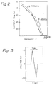
- Fig. 2 illustrates the characteristic curve of the current passed when 1 V is applied on the probe electrode when the distance between the probe electrode and the sample (recording layer) is varied.
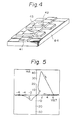
- Fig. 3 illustrates the pulse voltage waveform for recording.
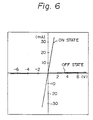
- Fig. 4 is a schematic illustration of MIM device.
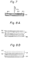
- Figs. 5 and 6 are characteristic graphs showing electrical characteristics obtained in the device shown in Fig. 4.
- Fig. 7 is a schematic illustration of the device for forming built-up film.
- Figs. 8A and 8B are schematic illustrations of a monomolecular film.
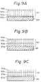
- Figs. 9A to 9C are schematic illustrations of a built-up film.
- Fig. 10A illustrates diagramatically the current passage recording and reproducing device of the present invention.
- Fig. 10B is a perspective view of a substrate on which a plural number of probes were provided
- Fig. 10C is a side view thereof.
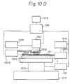
- Fig. 10D illustrates diagramatically another current passage recording and reproducing device of the present invention.
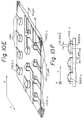
- Fig. 10E is a perspective view of a substrate on which a plural number of probes are provided, and Fig. 10F is a side view thereof.
- Figs. 11A to 11C illustrate schematically the track and the recorded state of data in the recording medium.
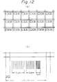
- Fig. 12A is a schematic illustration of the recording pattern used in the present invention.
- Fig. 12B is an enlarged view of the line pattern recorded within each lattice.
- the recording medium of the present comparative example by employing an organic built-up film with molecules having a group having ⁇ -electron level and a group having only ⁇ -electron level in combination laminated on an electrode, can exhibit a non-linear current-voltage characteristic different from the prior art by applying current by use of a probe electrode vertical to the film surface.
- the structure of the dye having ⁇ -electron system suitable for the comparative example there may be included, for example, dyes having porphyrine skeleton such as phthalocyanine, tetraphenylporphyrine, etc.; azulene type dyes having squarilium group and croconic methine group as the bonding chain and cyanine-like dyes having two or more nitrogen-containing heterocyclic rings such as quinoline, benzothiazole, benzoxazole, etc.
- cyanine dyes condensed polycyclic aromatic compounds such as anthracene and pyrene, and chain compounds obtained by polymerization of aromatic ring and heterocyclic compounds; and polymers of diacetylene group; further derivatives of tetraquinodimethane or tetrathiafluvalene and analogues thereof and charge transfer complexes thereof; and further metal complex compounds such as ferrocene, tris-bipyridine ruthenium complexes, etc.
- an LB method is extremely suitable among the known techniques because of controllability, easiness and reproducibility.
- a monomolecular film of an organic compound having a hydrophobic site and a hydrophilic site in one molecule or a built-up film thereof can be formed easily on a substrate, which has a thickness on the molecular order and a uniform and homogeneous organic ultra-thin film can be supplied stably over a large area.
- the LB method is a method in which a monomolecular film or its built-up film is prepared by utilizing the phenomenon that, in a molecule with a structure having a hydrophilic site and a hydrophobic site in a molecule, when the balance of the both (amphiphilic balance) is brought to a proper value, the molecule will form a layer of monomolecule on the water surface with the hydrophilic group directed downward.
- Examples of the group constituting the hydrophobic site may include various hydrophobic groups generally known widely such as saturated and unsaturated hydrocarbon groups, condensed polycyclic aromatic groups and chain polycyclic phenyl groups, etc. These may constitute the hydrophobic moiety each individually or as a combination of a plurality thereof.
- most representative as the constituent of the hydrophilic moiety are, for example, hydrophilic groups such as carboxyl group, ester group, acid amide group, imide group, hydroxyl group, further amino groups (primary, secondary, tertiary, and quaternary), etc. These also constitute the hydrophilic moiety of the above molecule each individually or as a combination of a plurality thereof.
- a dye molecule having these hydrophobic group and hydrophilic group in a well-balanced state and having ⁇ -electron system having an appropriate size can form a monomolecular film on the water surface, and it can be an extremely suitable material for the comparative example.
- R 1 corresponds to the group having ⁇ -electron level as mentioned above, and may be preferably a long chain alkyl group introduced with the carbon number n being 5 ⁇ n ⁇ 30 for making easier formation of the monomolecular film on the water surface.
- the compounds mentioned above as specific examples show only the basic structures, and various derivatives of these compounds are also suitable in the comparative example, as a matter of course.
- R is introduced for making easier formation of the monomolecular film, and is not limited to the substituents mentioned here.
- R 1 - R 4 correspond to the group having ⁇ -electron level as mentioned above.
- X is a hydrophilic group, and generally -COOH is used, but -OH, -CONH 2 , etc. can be also used.
- Dye materials suitable for the LB method other than those as mentioned above are of course suitable for the comparative example.
- biological materials of which study is becoming popular e.g. bacteriorhodopsin or cytochrome c
- synthetic polypeptides PBLG, etc.
- Amphiphilic molecule can form a monomolecular film with the hydrophilic groups directed downward.
- the monomolecular layer on the water surface has the characteristics of the two-dimensional system.
- k is the Boltzmann's constant
- T is an absolute temperature.
- A is made sufficiently small, intermolecular interactions are strengthened, whereby the molecules become a "condensed film (or solid film)"which acts like a two-dimensional solid.
- the condensed film can be transferred, one layer by one layer, onto the surface of any desired body having various materials and shapes such as glass or resin. By use of this method, a monomolecular film or built-up films thereof can be prepared, and used as the recording layer.
- a desired organic compound is dissolved in a solvent such as chloroform, benzene, acetonitrile, etc.
- a solvent such as chloroform, benzene, acetonitrile, etc.
- such solution is spread on an aqueous phase 81 by means of an appropriate device as shown in Fig. 7 in the accompanying drawings to form a layer or film 82 of the organic compound.
- a partitioning plate (or a float) 83 is provided to prevent too broad expansion of the spreading layer 82 through free diffusion on the aqueous phase 81, whereby the spreading area of the spreading film 82 is restricted to control the gathered state of the film substance and obtain a surface pressure ⁇ in proportion to the gathered state.
- the gathered state of the film substance can be controlled by reducing the spreading area, whereby the surface pressure can be gradually elevated to be set at a surface pressure suitable for preparation of the film.
- the surface pressure kept constant, by moving vertically a clean substrate 84 gently, a monomolecular film of an organic compound is transferred onto the substrate 84.
- Such monomolecular film 91 is a film having molecules orderly arranged as shown in Fig. 8A or 8B.
- the monomolecular film 91 can be thus produced, and a built-up film with desired built-up number can be formed by repeating the above operation.
- a built-up film with desired built-up number can be formed by repeating the above operation.
- other than the above vertical dipping method such methods as the horizontal lifting method, the rotating cylinder method, etc., may be employed.
- the horizontal lifting method is a method in which transfer is effected with the substrate being contacted horizontally on the water surface
- the rotating cylinder method is a method in which the monomolecular layer is transferred onto the substrate surface by rotating a cylindrical substrate on the water surface.
- a monomolecular film 91 of the organic compound with the hydrophilic sites 92 of the organic compound directed toward the substrate 84 side is formed on the substrate 84 (Fig. 8B).
- monomolecular films 91 are laminated one layer by one layer in the respective steps to form a built-up film 101. Since the direction of the film forming molecules in the withdrawing step becomes opposite to that of the dipping step, there is formed a Y type film according to this method in which the hydrophobic sites 93a and 93b of the organic compound are faced to each other between the respective layers (Fig. 9A).
- the monomolecular film 91 is formed on the substrate 84 with the hydrophobic site 93 of the organic compound faced toward the substrate 84 side (Fig. 8A).
- this method even when the monomolecular film 91 may be built up, there is no change in direction of the film forming molecules, but there is formed an X type film in which the hydrophobic sites 93a and 93b are faced toward the substrate side in all of the layers (Fig. 9B).
- a built-up film 101 in which the hydrophilic sites 92a and 92b are faced toward the substrate 84 side is called a Z type film (Fig. 9C).
- the method for transferring the monomolecular film 91 onto a substrate 84 is not limited to the above methods, but it is also possible to employ a method in which a substrate is extruded into an aqueous phase from a roll, when employing a large area substrate.
- the direction of the hydrophilic groups and the hydrophobic groups toward the substrate as described above are given as a general rule, and it can also be modified by the surface treatment of the substrate, etc.
- a potential barrier layer comprising the monomolecular film 91 of an organic compound or its built-up film is formed on the substrate 84.
- the substrate 84 for supporting the thin film comprising a lamination of the inorganic material and organic material may be any of metal, glass, ceramics, plastic materials, etc., and further a biological material with remarkably lower heat resistance can also be used.
- the substrate 84 as described above may be in any desired shape, preferably in a flat plate, which is not limitative of the comparative example at all. This is because the above film forming method has such advantage that the film can be formed exactly in accordance with the shape of the substrate surface independently of the shape of the substrate surface.
- tunnel current flows when the probe of a metal and an electroconductive substance are brought close to each other to a distance of about 1 nm with application of a voltage therebetween.
- This tunnel current depends on the work function on the surface, and therefore information regarding various surface electron states can be read.
- the method by use of tunnel current has a number of advantages such that it requires no vacuum condition, is applicable to both single crystalline and amorphous materials, has high resolving power, and yet reproduction at low power is possible without giving damage by the current.
- the recording medium may be one having a conductivity of 10 -10 (ohm.cm) -1 or higher, preferably 10 -8 (ohm.cm) -1 or higher.
- amorphous semiconductors such as chalcogenide glass containing Se, Te, as compounded with the element of the group III, IV, V or VI of the periodic table, etc. They are intrinsic semiconductors having an optical band gap Eg of 0.6 to 1.4 eV or an electrical activation energy ⁇ E of approximately 0.7 to 1.6 eV.
- chalcogenide glass of Ge-Sb-Se type may be also used.
- the electric memory effect of the medium can be exhibited.
- the object of the present invention can be sufficiently accomplished according to the thin-filmforming technique known in the art.
- suitable film-forming methods may include the vacuum vapor deposition method, the cluster ion beam method, etc.
- the electric memory effect of such material is observed at a film thickness of several pm or less, and concerning recording resolving power as the recording medium, the thickness may be preferably thinner.
- a film thickness is preferably 100 ⁇ to 1 ⁇ m more preferably a thickness of 1000 ⁇ or less.
- organic semiconductor layers having deposited a salt of an electron accepting compound such as tetraquinodimethane (TCNQ), TCNQ derivatives, for example, tetrafluorotetracyanoquinodimethane (TCNQF 4 ), tetracyanoethylene (TCNE) and tetracyanonaphthoquinodimethane (TNAP), etc. with a metal having relatively lower reduction potential such as copper or silver on the electrode.
- TCNQ tetraquinodimethane
- TCNQF 4 tetrafluorotetracyanoquinodimethane
- TCNE tetracyanoethylene
- TNAP tetracyanonaphthoquinodimethane
- the method for forming such organic semiconductor layer there may be employed the method in which the above electron accepting compound is vacuum vapor deposited on the electrode of copper or silver.
- the electric memory effect of such organic semiconductor is observed at a film thickness of several ten ⁇ m or less, but a film thickness of 100 ⁇ to 1 ⁇ m is preferred with respect to film forming property and uniformity.
- the material there may be employed (3) recording medium using amorphous silicon as the material.
- it is a recording medium having a layer constitution of metal/a-Si (p + layer/n layer/i layer) or metal/a-Si (n + layer/p layer/i layer), and the respective layers of a-Si can be deposited satisfactorily according to the methods known In the art.
- the glow discharge method (GD) may be preferably employed.
- the film thickness of a-Si may be preferably 2000 ⁇ to 8000 ⁇ for the n layer, about 1000 ⁇ for the p + layer, with the total film thickness being preferably about 0.5 ⁇ m to 1 ⁇ m.
- the electrode material to be used in the present invention may be one having high conductivity, including a large number of materials, typically metals such as Au, Pt, Ag, Pd, Al, In, Sn, Pb, W, etc. and alloys of these, further graphite or silicide, and further electroconductive oxides such as ITO, and application of these materials for the present invention may be contemplated.
- the method for forming electrodes by use of such material may be sufficiently the known thin film forming technique.
- an electroconductive material of which the surface will not form an insulating oxide film during formation of an LB film for example a noble metal or an oxide conductor such as ITO.
- the metal electrode of the recording medium is required if the recording layer in the present invention is insulating, but no such metal electrode is required if said recording layer exhibits semiconductive properties of M ⁇ or less.
- the recording layer itself can be used as the counter-electrode of the probe electrode.
- the tip of the probe electrode is required to be pointed so far as possible in order to enhance resolving power of recording/reproduction/ erasing.
- a platinum with a thickness of 1 mm in diameter with a tip mechanically ground to a cone of 90°, which is subjected to evaporation of the surface atoms by applying an electrical field in ultra-high vacuum is employed, but the shape of the probe and the treating method are not limited thereto.
- a device with MIM structure as shown in Fig. 4 was prepared, whereby a memory switching device exhibiting the current-voltage characteristics as shown in Fig. 5 and Fig. 6 was obtained, and the two states (ON state and OFF state) were already found to have respective memory characteristics.
- These memory switching characteristics appear at the layer thickness of several ⁇ to several 1000 ⁇ , but the recording medium used with the probe electrode should preferably have a layer thickness in the range of several ⁇ to 500 ⁇ , most preferably a layer thickness of 10 ⁇ to 200 ⁇ .
- 84 represents a substrate, 41 an Au electrode, 42 an Al electrode and 43 a built-up monomolecular film as described above.
- Fig. 1 is a block constituting diagram showing the recording device of the present invention.
- 105 is a probe current amplifier
- 106 a servo circuit for controlling the fine mechanism 107 by use of a piezoelectric element so that the probe current may become constant.
- 108 is a power source for applying a pulse voltage for recording/erasing between the probe electrode 102 and the electrode 103.
- the servo circuit 106 controls the HOLD circuit to be set ON so that the output voltage may be kept constant during that period.
- 109 is an XY scanning driving circuit for movement control of the probe electrode in the XY direction.
- 110 and 111 are used for coarse control of the distance between the probe electrode 102 and the recording medium 1 so that a probe current of about 10 -9 A may be obtained.
- These respective instruments are under the central control by means of a microcomputer 112.
- 113 has a display instrument.
- Fig. 10A is a block constituting diagram showing another recording device of the present invention.
- 1005 is a probe current amplifier
- 1006 is a servo circuit for controlling the fine mechanism 1007 by use of a piezoelectric element so that the probe current may become constant.
- 1008 is a power scurce for applying a pulse voltage for recording/erasing between the probe electrodes 1002a, b, c and the electrode 1003.
- the servo circuit 1006 controls the HOLD circuit to be set ON so that the output voltage may be kept constant during that period.
- 1009 is an XY scanning driving circuit for movement control of the probe electrodes 1001a, b, c in the XY direction.
- 1010 and 1011 are used for coarse control of the distance between the probe electrodes 1002a, b, c and the recording medium 1 so that a probe current of about 10-9 A may be previously obtained.
- These respective instruments are all under central control by means of a microcomputer 1012.
- 1013 represents a display instrument, and 1015 a wiring.
- Fig. 10D is another preferable example of the present invention, showing a block diagram of the device having a large number of probe electrodes 1002 provided, Fig. 10E showing a perspective view of an embodiment in which a number of probe electrodes 1002 are provided on the SiO 2 substrate and Fig. 10F showing a side view thereof.
- the probe electrodes shown in Figs. 10D - 10E can be prepared in a large number by implanting silicon onto the SiO 2 plate by focus-ion beam and permitting tungsten to grow selectively on the silicon.
- an A/D transducer 1016 for converting analog signals obtained to digital signals can be used.
- a high density record written by use of an energy beam such as a particle beam (an electron beam, or an ion beam) or a higher energy electromagnetic wave ray such as an X-ray, etc. and visible light, an UV-ray or a laser beam, etc. can be electrically reproduced by use of a probe electrode.
- an energy beam such as a particle beam (an electron beam, or an ion beam) or a higher energy electromagnetic wave ray such as an X-ray, etc. and visible light, an UV-ray or a laser beam, etc.
- the recording medium 1 to be used is constituted of a substrate electrode 103 and a recording layer 101 formed thereon.
- an inorganic or organic semiconductive substance can be used as the recording layer 101 mentioned above.
- inorganic semiconductors may include semiconductive substances containing the element selected from the group IVB of the long period type periodic table (C, Si, Ge), semiconductive substances containing the element selected from the group IIIB (Ga) and the element selected from the group VB (As, P) or semiconductive substances containing the element selected from the group IIB (Zn, Cd) and the element selected from the group VIB (O, S, Se).
- typically semiconductors such as Si (single crystalline, polysilicon, amorphous), Ge, GaAs, GaP, InAs, InP or CdS, CdSe, ZnO, ZnS, etc.
- organic semiconductors may include a large number of organic semiconductors, for example, aromatic polycyclic compounds such as phthalocyanine and derivatives thereof, pyrene, perylene, etc. and derivatives thereof; polymeric compounds having conjugated ⁇ bond such as polyacetylene, polydiacetylene derivatives, etc.; further electrolytic polymerized films such as of pyrrole, thiophene, etc.; or polyvinyl carbazole, tetraquinodimethane, docosylpyridinium, tetraquinodimethane charge transfer complexes, etc.
- aromatic polycyclic compounds such as phthalocyanine and derivatives thereof, pyrene, perylene, etc. and derivatives thereof
- polymeric compounds having conjugated ⁇ bond such as polyacetylene, polydiacetylene derivatives, etc.
- further electrolytic polymerized films such as of pyrrole, thiophene, etc.
- polyvinyl carbazole tetraquinodime
- These semiconductor substances can be formed in conventional manner into thin films.
- an inorganic semiconductor there can be employed the vacuum vapor deposition method, the sputtering method, the glow discharge method, etc.
- the vacuum vapor deposition method such as the cluster ion beam method or the electrolytic polymerization method may be available.
- film formation can be effected by coating of a coating liquid having a semiconductive substance dispersed in an appropriate resin (e.g. polystyrene, polyacrylonitrile, polycarbonate, polyester, etc. according to a conventional method (roll coating, dip coating, etc.).
- an appropriate resin e.g. polystyrene, polyacrylonitrile, polycarbonate, polyester, etc.
- a Langmuir-Blodgett method (an LB method) proposed by Langmuir et al as described above is applicable.
- the molecules as shown below may be included.
- polypeptides such as bacteriorhodopsin or cytochrome c
- synthetic polypeptides PBLG, etc.
- a potential barrier layer comprising a monomolecular film of such organic compound or its built-up film is formed on the substrate.
- the substrate for supporting the thin film comprising a laminate of inorganic and organic materials as described above may be any of metal, glass, ceramics, plastic materials, etc., and further a biological material with remarkably lower heat resistance can be also used.
- the substrate as mentioned above may have any desired shape, preferably a flat plate shape, but the shape is not limited to a flat plate at all.
- the film forming method irrespectively of whether the substrate may have any surface shape, there is the advantage that the film can be formed exactly the same as its shape.
- the recording layer 101 can be recorded with various energy beams as described below, and the recorded image can be reproduced by means of the reproducing means as described above. In the following, specific examples of the recording method are shown.
- the thin film structure change of an LB film, etc. as mentioned here may sometimes occur alone, but in many cases some effects will generally occur associatedly.
- the electrode for laminating a thin film such as an LB film, etc. as described above, all conductors having conductivity of 10-6 (ohm.cm)-1 or higher can be used. More specifically, with the use of a metal plate such as Au, Pt, Pd, Ag, Al, or a glass, ceramics, plastic materials having these metals vapor deposited thereon, or semiconductors such as Si (crystalline, amorphous) as the substrate, a thin film such as LB film can be laminated thereon and used as the recording medium.
- a metal plate such as Au, Pt, Pd, Ag, Al, or a glass, ceramics, plastic materials having these metals vapor deposited thereon, or semiconductors such as Si (crystalline, amorphous) as the substrate.
- a recording/reproducing device shown in Fig. 1 was employed.
- the probe electrode 102 a probe electrode made of platinum was used. This probe electrode 102 is used for controlling the distance (Z) from the surface of the recording layer 101, and its distance (Z) is finely controlled by a piezoelectric element so that the current may be controlled to be constant. Further, the fine control mechanism 107 is designed so that fine movement control may be possible also in the plane (X,Y) direction. However, all of these are known techniques. Also, the probe electrode 102 can be used for direct recording, reproduction and erasing. The recording medium is placed on the XY stage 114 with high precision and can be moved to any desired position.
- a recording medium 1 having a recording layer with 8 built-up SOAZ layers was placed on the XY stage 114, and first the position of the probe electrode 102 was determined and fixed firmly. Between the Au electrode (the ground side) 103 and the probe electrode 102, a voltage of -3.0 V was applied, and the distance (Z) between the probe electrode 102 and the recording layer 101 surface was controlled while monitoring the current. Thereafter, the distance from the probe electrode 102 to the surface of the recording layer 101 was changed by controlling the fine control mechanism 107, whereby the current characteristics as shown in Fig. 2 were obtained.
- the probe voltage should be controlled so that the probe current Ip for controlling the distance from the probe electrode 102 to the surface of the recording layer 101 may be 10 -7 A ⁇ Ip ⁇ 10 -12 A, preferably 10 -8 A ⁇ Ip ⁇ 10 -10 A.
- the controlled current was set to be current value of the a region in Fig. 2 (10 -7 A) - (Condition of probe grounding).
- the current value was measured by applying reading voltage of 1.5 V which was a voltage not exceeding the threshold voltage which gives rise to electric memory effect between the probe electrode 102 and the Au electrode 103, OFF state was exhibited at ⁇ A or less.
- the current was again measured by applying a voltage of 1.5 V between the electrodes, whereby a current of about 0.7 mA was found to flow, thus indicating the ON state.
- the distance Z between the probe electrode 102 and the surface of the recording layer 101 was controlled.
- the resolving power was measured by writing stripes of 1 ⁇ length with various pitches between 0.001 ⁇ and 0.1 ⁇ , and it was found to be 0.01 ⁇ or less.
- the SOAZ-LB film used in the above experiments was prepared as described below.
- Evaluation was performed overall from the recording and erasing characteristics after applying the pulse and the erasing voltage, further the ratio of the current value under the recording state to that of the erased state (ON/OFF) and the resolving ability, and those with particularly good results were rated as A, those with excellent results as B, and those with relatively somewhat lower results as compared with others as C.
- Recording media were prepared by use of the substrate electrode materials and the dye compounds shown in Table 2, and the same experiments as in Comparative Examples 1 and 2 were conducted with the controlled current value of the probe current set at 10 -9 A to obtain the results shown in Table 2. As shown by the mark B in the Table, recording and reproduction could be done at sufficient resolving power and ON/OFF ratio for all of the samples.
- the built-up number of the dye LB film was all two layers. Also, the Pt electrode was vapor deposited by use of the EB method, and ITO by the sputtering method, respectively.
- the LB method was employed for formation of the dye recording layer, but any film forming method can be used without limitation to the LB method, provided that an extremely thin film can be prepared, and specifically the vacuum vapor deposition method such as MBE, CVD method, etc. may be included.
- Applicable materials are not limited to only organic compounds, but inorganic materials such as chalcogenide compounds, etc. are also applicable.
- the electrode and the recording layer by use of a semiconductor as the electrode on the recording medium side.
- the present invention is not limited to the use of any particular substrate material, shape or surface structure.
- a recording/reproducing device shown in and described with reference to Fig. 1 was employed.
- the probe electrode 102 a probe electrode made of platinum was used and recording, reproduction and erasure experiments were carried out using as the recording layer 101 a chalcogenide glass represented by the composition formula Si 16 Ge 14 As 5 Te 65 (the subscripts correspond to atomic%) (film thickness 2000 ⁇ ) formed on the electrode 103 formed of Au.
- a recording medium 1 having a recording layer 101 of the above chalcogenide glass having a thickness of 2000 ⁇ was placed on the XY stage 114. Between the Au electrode (the ground side) 103 and the probe electrode 102, a voltage of 1.0 V was applied, and the distance (Z) between the probe electrode 102 and the recording layer 101 surface was controlled while monitoring the current. Thereafter, the fine control mechanism 107 was controlled so that the probe current Ip became 10 -9 A.
- the probe voltage should be controlled so that the probe current Ip for controlling the distance from the probe electrode 102 to the surface of the recording layer 101 may be 10 -7 A ⁇ Ip ⁇ 10 -12 A, preferably 10 -8 A ⁇ Ip ⁇ 10 -10 A.
- the resolving power was measured by writing stripes of 1 ⁇ length with various pitches between 0.01 ⁇ and 1 ⁇ , and it was found to be 0.1 ⁇ or less.
- the chalcogenide glass used in the above experiments was prepared as described below.
- an amorphous semiconductor represented by the atomic composition ratio of Si 16 Ge 14 As 5 Te 65 was vapor deposited to a film thickness of 2000 ⁇ by the vacuum vapor deposition method known in the art and used as the recording medium.
- Example 1 The same experiment as in Example 1 was conducted except for using Ge 15 Te 81 Sb 2 S 2 in place of Si 16 Ge 14 As 5 Te 65 used in Example 1. It was found that writing and reading of record could be done at sufficient S/N ratio similarly as in Comparative Example 1.
- Cu was deposited to 2000 ⁇ according to the vacuum vapor deposition method to provide an electrode. Further, Cu and TCNQF 4 were co-deposited by the vacuum vapor deposition method to deposite a Cu-TCNQF 4 layer to 2000 ⁇ (substrate temperature; room temperature). At this time, heating was effected by passing current value previously set so that the vapor deposition speed may become about Cu, 5 ⁇ /s; TCNQF 4 , 20 ⁇ /s. As the result, it was confirmed that a blue film by formation of CuTCNQF 4 was deposited.
- any film forming method capable of preparing an extremely uniform film can be used and is not also limitative of the substrate material, its shape and surface structure at all.
- a recording/reproducing device shown in Fig. 10 was employed.
- the probe electrodes 1002a, b, c three tungsten probe electrodes 3 were employed.
- the probe electrodes 1002a, b, c were used for controlling the distance (Z) from the surface of the recording layer 101, and its distance (Z) is finely controlled by a piezoelectric element so that the current may be controlled to be constant.
- the fine control mechanism 1007 is designed so that fine control may be possible also in the plane (X,Y) direction. However, all of these are known techniques.
- the probe electrodes 1002a, b, c can be used for direct recording, reproduction and erasing.
- the recording medium is placed on the XY stage 1014 with high precision and can be moved to any desired position.
- a recording medium 1 having a recording layer 101 with 8 built-up SOAZ layers was placed on the XY stage 1014, and first the positions of the probe electrodes 1002a, b, c were determined and fixed firmly. Between the Au electrode (the ground side) 1003 and the probe electrode 1002, a voltage of -3.0 V was applied, and the distance (Z) between the probe electrode 1002 and the recording layer 101 surface was controlled while monitoring the current. Thereafter, the distance from the probe electrode 1002 to the surface of the recording layer 101 was changed by controlling the fine control mechanism 1007, whereby the current characteristics as shown in Fig. 2 were obtained.
- the probe voltage should be controlled so that the probe current Ip for controlling the distance from the probe electrode 1002 to the surface of the recording layer 101 may be 10 -7 A ⁇ Ip ⁇ 10 -12 A, preferably 10 -8 A ⁇ Ip ⁇ 10 -10 A.
- the controlled current was set to the current value of the a region in Fig. 2 (10 -7 A) - (Condition of probe grounding).
- the current value was measured by applying reading voltage of 1.5 V which was a voltage not exceeding the threshold voltage which gives rise to electric memory effect between the probe electrode 1002 and the Au electrode 1003, OFF state was exhibited at ⁇ A or less.
- the current was again measured by applying a voltage of 1.5 V between the electrodes, whereby a current of about 0.7 mA was found to flow, thus indicating the ON state.
- the distance Z between the probe electrode 1002a, b, c and the surface of the recording layer 101 was controlled.
- the probes 1002 a, b and c were returned to the original positions, then while applying a triangular pulse voltage having the waveform as shown in Fig. 3 which is a voltage of the threshold voltage Vth ON or higher at which the ON state occurs at the two probes (1002-a, c) along the X-axis, track signals along the X-axis were recorded (Fig. 11B).
- the remaining one probe (1002-b) wrote the ON state by applying a pulse voltage (15 Vmax, 1 ⁇ S) of the threshold voltage Vth, ON or higher having the same waveform as in Fig. 3 at the predetermined position of the timing signal, and also the data were recorded at the remaining sites by use of the same method.
- the probe 1002-a was moved along the Y-axis to the track recorded with the probe 1002-c, and the same operation as described above was conducted. At this time, only the probe 1001a performs reading of the track signal. Subsequently, this operation was repeated until a recording medium having the track signals and the data recorded thereon was prepared (Fig. 11C).
- Reading can be done by applying a probe voltage of 1.5 V for reading between the probe electrode 1002-b and the counter-electrode 1003, and reading directly the change in current quantity passing between the ON state region and OFF state region or through the servo circuit 1006.
- the probe current passing through the ON state region was found to be changed by 3 digits or more as compared with that before recording (or the OFF state region).
- the resolving power was measured by writing stripes of 1 ⁇ length with various pitches between 0.001 ⁇ and 0.1 ⁇ , and it was found to be 0.01 ⁇ or less.
- the SOAZ-LB film used in the above experiments was prepared as described in Comparative Example 1.
- the evaluation results are shown in Table 3 and the basis of evaluation (A, B, or C) is as described in Comparative Example 1.
- Recording media were prepared by use of the substrate electrode materials and the dye compounds shown in Table 4, and the same experiments as in Comparative Examples 12 and 13 were conducted with the controlled current value of the probe current set at 10 -9 A to obtain the results shown in Table 4. As shown by the mark B in the Table, recording and reproduction could be done at sufficient resolving power and ON/OFF ratio for all of the samples.
- the built-up number of the dye LB film was all two layers. Also, the Pt electrode was vapor deposited by use of the EB method, and ITO by the sputtering method, respectively.
- the LB method was employed for formation of the dye recording layer, but any film forming method can be used without limitation to the LB method, provided that an extremely thin film can be prepared, and specifically the vacuum vapor deposition method such as an MBE method, a CVD method, etc. may be included.
- Applicable materials are not limited to only other organic compounds, but inorganic materials such as chalcogenide compounds, etc. are also applicable.
- the present invention is not limitative of the substrate material, its shape and surface structure at all. Also, although three probes are used in this Example, the number of probes can also be greater than three.
- Such polymerizable recording medium was mounted on ELS-3300 electron beam picture drawing device produced by Elionics Co., and a picture was drawn by use of a lattice pattern generating device shown in Fig. 12A under the conditions of an acceleration voltage of 20 kV, a current value of 1 x 10 -9 A, a stationary spot diameter of 0.4 ⁇ m, an exposure time of 0.5 ⁇ sec/spot.
- the magnification at this time was 50-fold.
- the pattern thus drawn was read by use of a reproducing device shown in Fig. 1. Next, its process is shown.
- the position of the probe electrode was determined by visual observation.
- the distance between the probe electrode and the recording medium was controlled so that the probe current became 10 -9 A by controlling the coarse mechanism in the Z direction.
- the line pattern was read by fine scanning within the plane (x, y). It was found that the portion irradiated by the electron beam was polymerized and its film thickness was recognized to be changed (reduced) by about several ⁇ as calculated on the changed amount of servo voltage. Also, the line width read was 0.022 ⁇ m and thus it was found that at least a recording resolving power of about 0.02 ⁇ m could be obtained.
- the DA12-8 recording medium used in the above experiment was prepared as described below.
- the surface pressure was enhanced to 20 mN/m, and further while maintaining the pressure to be constant, the above electrode substrate was dipped gently so as to transverse across the water surface and further withdrawn to build up two layers of a monomolecular film.
- the DA12-8 monomolecular built-up film thus formed on the Au electrode was dried on air for 24 hours to provide a recording medium.
- the LB film forming conditions of ⁇ -tricosenic acid were as follows.
- perylenetetracarboxylic acid anhydride was vacuum vapor deposited (vapor deposition speed 5 ⁇ /sec, film thickness 300 ⁇ ) to provide a recording medium, and otherwise the same recording and reproducing experiment as in Example 36A was conducted.
- the electron beam irradiated portion was recognized to be blackened.
- the line width reproduced with a probe voltage of 2V was found to be 0.04 ⁇ m.
- the pattern shown in Fig. 12 was drawn on a p-form ⁇ 111> wafer substrate (10 ohm-cm) in the same manner as in Example 24 by injecting P + ions by means of a converging ion beam device JIBL produced by Nippon Denshi K.K.
- the injection conditions were as follows.
- the pattern in Fig. 12 was drawn by injecting I - ions by means of the same converging ion beam device in the same manner as in Comparative Example 26 on a recording medium having 13 layers of tetraquinodimethane docosylpyridium built up on an optically polished glass substrate.
- the injection conditions were ion source acceleration voltage 40 kV, ion beam current 1000 pA, injected amount 5 x 10 13 ions/cm 2 , and substrate temperature 20°C.
- the line width was found to be 0.1 ⁇ m on an average.
- electron beam and ion beam were used as the energy beam, but the energy beam is not limited to these, but electromagnetic waves such as visible light, UV-ray and X-ray, etc. can be also used.
- the SOAZ-LB film used in the above experiments was prepared as described below.
- an optically polished glass substrate substrate 1004 was washed by use of a neutral detergent and Trichlene, Cr was deposited as the subbing layer by the vacuum deposition method to a thickness of 50 ⁇ , and further Au was vapor deposited by the same method to 400 ⁇ to form a subbing electrode (Au electrode 1003).
- Evaluation was performed overall from the recording and erasing characteristics after applying the pulse and the erasing voltage, further the ratio of the current value under the recording state to that of the erased state (ON/OFF) and the resolving power, and those with particularly excellent results were rated as A, those with good results as B, and those with relatively somewhat lower results as compared with others as C.
- Recording media were prepared by use of the substrate electrode materials and the dye compounds shown in Table 8, and the same experiments as in Comparative Examples 28 and 29 were conducted with the controlled current value of the probe current set at 10 -9 A to obtain the results shown in Table 8. As shown by the mark B in the Table, recording and reproduction could be done at sufficient resolving power and ON/OFF ratio for all of the samples.
- the built-up number of the dye LB film was all two layers. Also, the Pt electrode was vapor deposited by use of the EB method, and ITO by the sputtering method, respectively.
- the LB method was employed for formation of the dye recording layer, but any film forming method can be used without limitation to the LB method, provided that an extremely thin film can be prepared, and specifically the vacuum vapor deposition method such as an MBE method, a CVD method, etc. may be included.
- Applicable materials are not limited to only organic compounds, but inorganic materials such as chalcogenide compounds, etc. are also applicable.
- the present invention is not limitative of the substrate material, its shape and surface structure at all. More than three probes may be employed although three probes were emploved in this example.
- Embodiments of the invention enable a novel recording and reproducing device having the following specific features to be provided.
Landscapes
- Chemical & Material Sciences (AREA)
- Physics & Mathematics (AREA)
- Engineering & Computer Science (AREA)
- Organic Chemistry (AREA)
- General Physics & Mathematics (AREA)
- Nanotechnology (AREA)
- Mathematical Physics (AREA)
- Theoretical Computer Science (AREA)
- Crystallography & Structural Chemistry (AREA)
- Semiconductor Memories (AREA)
- Thermal Transfer Or Thermal Recording In General (AREA)
- Optical Record Carriers And Manufacture Thereof (AREA)
Claims (20)
- Système pour la reproduction d'informations, le système comportant une électrode de sonde (102 ; 1002), un support d'enregistrement (1) disposé de façon à être opposé à l'électrode de sonde (102 ; 1002) afin qu'un courant puisse circuler par effet tunnel lorsqu'une tension est appliquée entre eux ; des moyens destinés à appliquer une tension de lecture entre l'électrode de sonde (102) et le support d'enregistrement (1 ; 101) pour détecter ainsi un courant circulant par effet tunnel entre le support et l'électrode de sonde (102 ; 1002) afin de détecter des informations enregistrées sur celui-ci, le système étant caractérisé en ce que le support d'enregistrement est un semiconducteur amorphe, formé de verre de chalcogénure contenant au moins un élément des Groupes III, IV, V et VI du Tableau Périodique et au moins l'un de Se, Te et As.
- Système selon la revendication 1, comprenant des moyens destinés à appliquer une tension d'écriture entre l'électrode de sonde (102 ; 1002) et le support d'enregistrement (1 ; 101) pour enregistrer ainsi des informations sur le support d'enregistrement en utilisant l'effet de mémoire électrique.
- Système selon la revendication 1 ou la revendication 2, dans lequel le support d'enregistrement (101) est un film ou une couche sur la surface d'un substrat (103).
- Système selon l'une quelconque des revendications précédentes, comportant en outre des moyens (107, 1007) destinés à régler les positions relatives entre l'électrode de sonde (102 ; 1002) et le support d'enregistrement (1, 101).
- Système selon la revendication 4, dans lequel les moyens de réglage (107, 1007) sont agencés de façon à régler les positions relatives dans une direction parallèle à la surface du support d'enregistrement (1, 101).
- Système selon la revendication 5, dans lequel les moyens de réglage comprennent des moyens de balayage X,Y pour l'électrode de sonde (102, 1002).
- Système selon l'une quelconque des revendications 4 à 6, dans lequel les moyens de réglage (107, 1007) sont agencés de façon à régler les positions relatives dans une direction normale à la surface du support d'enregistrement (1, 101).
- Système selon la revendication 7, dans lequel les moyens de réglage sont agencés de façon à maintenir une distance constante entre l'électrode de sonde (102, 1002) et la surface du support d'enregistrement pendant un enregistrement ou une reproduction d'informations (1, 101).
- Système selon l'une quelconque des revendications 4 à 8, dans lequel les moyens de réglage sont agencés de façon à réaliser un réglage fin dans trois dimensions entre les positions relatives de l'électrode de sonde (102, 1002) et du support d'enregistrement (1, 101).
- Système selon l'une quelconque des revendications précédentes, dans lequel les moyens (108 ; 1008) destinés à appliquer une tension de lecture comportent un circuit d'asservissement (106 ; 1006) pour la reproduction d'informations.
- Système selon l'une quelconque des revendications précédentes, dans lequel les moyens (1008) destinés à appliquer une tension de lecture comportent un transducteur A/N (1016) pour la reproduction d'informations.
- Système selon l'une quelconque des revendications précédentes, dans lequel la tension de lecture est appliquée en tant que tension de polarisation (108 ; 1008).
- Dispositif selon l'une quelconque des revendications précédentes, dans lequel la tension de lecture laisse intactes les informations enregistrées sur le support d'enregistrement (1, 101).
- Système selon l'une quelconque des revendications précédentes, comprenant des moyens (108 ; 1008) destinés à appliquer une tension d'écriture entre l'électrode de sonde (102, 1002) et le support d'enregistrement (1, 101), lesdits moyens étant agencés pour appliquer la tension d'écriture sous la forme d'une tension à impulsions.
- Système selon l'une quelconque des revendications précédentes, comportant en outre des moyens (108 ; 1008) destinés à effacer les informations enregistrées en appliquant une tension entre l'électrode de sonde (102, 1002) et la surface d'enregistrement (1, 101).
- Système selon l'une quelconque des revendications précédentes, dans lequel le support d'enregistrement (1, 101) comporte un film capable d'agir lui-même en tant qu'électrode.
- Système selon l'une quelconque des revendications précédentes, dans lequel plusieurs électrodes de sonde (1002a, 1002b, 1002c) sont prévues.
- Système selon l'une quelconque des revendications précédentes, dans lequel le support d'enregistrement est sélectionné parmi des verres des types As-Se-Te, Ge-As-Se, Si-Ge-As-Te et Ge-Te-X ou Si-Te-X où X est un élément du Groupe V ou VI.
- Procédé d'enregistrement d'informations, comprenant la mise en oeuvre d'un système selon l'une quelconque des revendications dépendantes de la revendication 2 pour enregistrer des informations.
- Procédé de reproduction d'informations comprenant la mise en oeuvre d'un système selon l'une quelconque des revendications 1 à 18 pour reproduire des informations.
Applications Claiming Priority (15)
| Application Number | Priority Date | Filing Date | Title |
|---|---|---|---|
| JP309433/86 | 1986-12-24 | ||
| JP61309433A JP2556491B2 (ja) | 1986-12-24 | 1986-12-24 | 記録装置及び記録法 |
| JP309434/86 | 1986-12-24 | ||
| JP61309434A JP2556492B2 (ja) | 1986-12-24 | 1986-12-24 | 再生装置及び再生法 |
| JP3613987A JPS63204531A (ja) | 1987-02-19 | 1987-02-19 | 再生装置 |
| JP36139/87 | 1987-02-19 | ||
| JP55851/87 | 1987-03-11 | ||
| JP5585287A JPS63222348A (ja) | 1987-03-11 | 1987-03-11 | 記録装置及び記録法 |
| JP62055851A JP2603241B2 (ja) | 1987-03-11 | 1987-03-11 | 記録装置および再生装置 |
| JP55852/87 | 1987-03-11 | ||
| JP19186387A JPS6435744A (en) | 1987-07-31 | 1987-07-31 | Reproducing device and reproducing method |
| JP191862/87 | 1987-07-31 | ||
| JP191863/87 | 1987-07-31 | ||
| JP62191862A JP2556520B2 (ja) | 1987-07-31 | 1987-07-31 | 記録装置及び記録法 |
| EP87311397A EP0272935B1 (fr) | 1986-12-24 | 1987-12-23 | Appareil d'enregistrement et appareil de reproduction |
Related Parent Applications (2)
| Application Number | Title | Priority Date | Filing Date |
|---|---|---|---|
| EP87311397A Division EP0272935B1 (fr) | 1986-12-24 | 1987-12-23 | Appareil d'enregistrement et appareil de reproduction |
| EP87311397.1 Division | 1987-12-23 |
Publications (3)
| Publication Number | Publication Date |
|---|---|
| EP0551966A2 EP0551966A2 (fr) | 1993-07-21 |
| EP0551966A3 EP0551966A3 (en) | 1993-09-15 |
| EP0551966B1 true EP0551966B1 (fr) | 1999-04-14 |
Family
ID=27564415
Family Applications (4)
| Application Number | Title | Priority Date | Filing Date |
|---|---|---|---|
| EP93200797A Expired - Lifetime EP0551966B1 (fr) | 1986-12-24 | 1987-12-23 | Appareil d'enregistrement et appareil de reproduction |
| EP93200792A Expired - Lifetime EP0555941B1 (fr) | 1986-12-24 | 1987-12-23 | Appareil d'enregistrement et appareil de reproduction |
| EP93200793A Expired - Lifetime EP0551964B1 (fr) | 1986-12-24 | 1987-12-23 | Appareil d'enregistrement et de reproduction |
| EP87311397A Expired - Lifetime EP0272935B1 (fr) | 1986-12-24 | 1987-12-23 | Appareil d'enregistrement et appareil de reproduction |
Family Applications After (3)
| Application Number | Title | Priority Date | Filing Date |
|---|---|---|---|
| EP93200792A Expired - Lifetime EP0555941B1 (fr) | 1986-12-24 | 1987-12-23 | Appareil d'enregistrement et appareil de reproduction |
| EP93200793A Expired - Lifetime EP0551964B1 (fr) | 1986-12-24 | 1987-12-23 | Appareil d'enregistrement et de reproduction |
| EP87311397A Expired - Lifetime EP0272935B1 (fr) | 1986-12-24 | 1987-12-23 | Appareil d'enregistrement et appareil de reproduction |
Country Status (3)
| Country | Link |
|---|---|
| US (1) | US5623476A (fr) |
| EP (4) | EP0551966B1 (fr) |
| DE (4) | DE3752099T2 (fr) |
Families Citing this family (89)
| Publication number | Priority date | Publication date | Assignee | Title |
|---|---|---|---|---|
| US5255258A (en) * | 1987-09-24 | 1993-10-19 | Canon Kabushiki Kaisha | Microprobe, preparation thereof and electronic device by use of said microprobe |
| US4906840A (en) * | 1988-01-27 | 1990-03-06 | The Board Of Trustees Of Leland Stanford Jr., University | Integrated scanning tunneling microscope |
| JP2756254B2 (ja) * | 1988-03-25 | 1998-05-25 | キヤノン株式会社 | 記録装置及び再生装置 |
| DE3823010A1 (de) * | 1988-07-07 | 1989-09-21 | Leitz Wild Gmbh | Anordnung zum auslesen von daten |
| JP2896794B2 (ja) * | 1988-09-30 | 1999-05-31 | キヤノン株式会社 | 走査型トンネル電流検出装置,走査型トンネル顕微鏡,及び記録再生装置 |
| EP0363147B1 (fr) * | 1988-10-04 | 1996-06-05 | Canon Kabushiki Kaisha | Appareil et procédé d'enregistrement et de reproduction et milieu d'enregistrement pour le procédé d'enregistrement et de reproduction |
| DE68928559T2 (de) * | 1988-12-15 | 1998-06-18 | Mitsui Toatsu Chemicals | Absorbiermittel im nahen Infrarot und Anzeige-/Aufzeichnungsmaterialien, die daraus hergestellt sind |
| JPH02187944A (ja) * | 1989-01-13 | 1990-07-24 | Sharp Corp | 再生装置 |
| JPH02206043A (ja) * | 1989-02-03 | 1990-08-15 | Olympus Optical Co Ltd | 記憶装置 |
| US5144581A (en) * | 1989-02-09 | 1992-09-01 | Olympus Optical Co., Ltd. | Apparatus including atomic probes utilizing tunnel current to read, write and erase data |
| US5289408A (en) * | 1989-02-09 | 1994-02-22 | Olympus Optical Co., Ltd. | Memory apparatus using tunnel current techniques |
| JP2714211B2 (ja) * | 1989-03-16 | 1998-02-16 | キヤノン株式会社 | 記録及び再生装置 |
| US5241527A (en) * | 1989-03-16 | 1993-08-31 | Canon Kabushiki Kaisha | Recording and reproducing apparatus and method using a recording layer having a positioning region |
| US5079958A (en) * | 1989-03-17 | 1992-01-14 | Olympus Optical Co., Ltd. | Sensor having a cantilever |
| DE69031053T2 (de) * | 1989-04-25 | 1998-01-29 | Canon Kk | Informationsaufzeichnungs-/Wiedergabegerät und Informationsaufzeichnungsträger |
| CA2022929C (fr) * | 1989-08-10 | 1995-02-07 | Hisaaki Kawade | Support d'enregistrement organique avec electrodes |
| JP2859715B2 (ja) * | 1989-08-10 | 1999-02-24 | キヤノン株式会社 | 記録媒体用基板及びその製造方法、記録媒体、記録方法、記録再生方法、記録装置、記録再生装置 |
| EP0416920B1 (fr) * | 1989-09-07 | 1996-01-03 | Canon Kabushiki Kaisha | Procédé et dispositif de traitement d'information |
| JP2910089B2 (ja) * | 1989-09-29 | 1999-06-23 | 松下電器産業株式会社 | 光学記録媒体の検出方法 |
| DE3943414A1 (de) * | 1989-12-30 | 1991-07-04 | Basf Ag | Verfahren zur speicherung von informationseinheiten im nanometerbereich |
| DE69127381T2 (de) * | 1990-01-19 | 1998-01-22 | Canon Kk | Informationsverarbeitungssystem und Informationsverarbeitungsmethode |
| US6308405B1 (en) | 1990-02-07 | 2001-10-30 | Canon Kabushiki Kaisha | Process for preparing an electrode substrate |
| JP2783646B2 (ja) * | 1990-04-18 | 1998-08-06 | キヤノン株式会社 | 情報記録再生装置 |
| JPH041949A (ja) * | 1990-04-18 | 1992-01-07 | Canon Inc | 情報入力及び/または取出し装置 |
| US5255259A (en) * | 1990-04-18 | 1993-10-19 | Canon Kabushiki Kaisha | Method of access to recording medium, and apparatus and method for processing information |
| JPH041948A (ja) * | 1990-04-18 | 1992-01-07 | Canon Inc | 情報記録装置及び情報再生装置及び情報記録再生装置 |
| DE4015656A1 (de) * | 1990-05-16 | 1991-11-21 | Basf Ag | Verfahren zur zeitlich stabilen markierung einzelner atome oder atomgruppen einer festkoerperoberflaeche sowie verwendung dieses verfahrens zur speicherung von informationseinheiten im atomaren bereich |
| DE4021077A1 (de) * | 1990-07-03 | 1992-01-09 | Basf Ag | Verfahren zur zeitlich stabilen markierung einzelner atome oder atomgruppen einer festkoerperoberflaeche sowie verwendung dieses verfahrens zur speicherung von informationseinheiten im atomaren bereich |
| JP2945090B2 (ja) * | 1990-07-09 | 1999-09-06 | キヤノン株式会社 | エンコーダ |
| JP2802828B2 (ja) * | 1990-10-19 | 1998-09-24 | キヤノン株式会社 | 情報記録担体及びこれを使用する情報処理装置 |
| CA2059990C (fr) * | 1991-01-29 | 1997-11-25 | Shun-Ichi Shido | Appareil et methode de deplacement et appareil de detection et(ou) de saisie de l'information utilisant le premier |
| JP2744359B2 (ja) * | 1991-04-24 | 1998-04-28 | キヤノン株式会社 | 情報再生及び/又は情報記録装置 |
| JP2930447B2 (ja) * | 1991-05-15 | 1999-08-03 | キヤノン株式会社 | 情報処理装置 |
| JP3198355B2 (ja) * | 1991-05-28 | 2001-08-13 | キヤノン株式会社 | 微小変位素子及びこれを用いた走査型トンネル顕微鏡、情報処理装置 |
| JP2794348B2 (ja) * | 1991-06-21 | 1998-09-03 | キヤノン株式会社 | 記録媒体、その製造方法、情報処理装置 |
| US5161149A (en) * | 1991-07-22 | 1992-11-03 | The Johns Hopkins University | Electron density storage device and method using STM |
| US5216661A (en) * | 1991-07-22 | 1993-06-01 | The Johns Hopkins University | Electron density storage device using a stm |
| JPH05282717A (ja) * | 1992-03-31 | 1993-10-29 | Canon Inc | 記録媒体の製造方法、及び記録媒体、及び情報処理装置 |
| DE69328364T2 (de) * | 1992-07-17 | 2000-12-28 | Biotechnology Research And Development Corp. Inc., Peoria | Lesen und schreiben von gespeicherter information mittels elektrochemie |
| US5434842A (en) * | 1992-07-17 | 1995-07-18 | Biotechnology Research And Development Corporation | Reading and writing stored information by means of electrochemistry |
| EP0901120A3 (fr) * | 1992-07-17 | 2001-01-10 | Biotechnology and Research and Development Corporation | Lecture et écriture par voie électrochimique d'informations stockées |
| JP3135753B2 (ja) * | 1993-08-26 | 2001-02-19 | キヤノン株式会社 | プローブを用いた記録再生方法および装置 |
| US5751683A (en) * | 1995-07-24 | 1998-05-12 | General Nanotechnology, L.L.C. | Nanometer scale data storage device and associated positioning system |
| US6339217B1 (en) * | 1995-07-28 | 2002-01-15 | General Nanotechnology Llc | Scanning probe microscope assembly and method for making spectrophotometric, near-field, and scanning probe measurements |
| US6337479B1 (en) * | 1994-07-28 | 2002-01-08 | Victor B. Kley | Object inspection and/or modification system and method |
| WO1996017345A1 (fr) * | 1994-11-29 | 1996-06-06 | Matsushita Electric Industrial Co., Ltd. | Procede d'enregistrement et de lecture d'informations et dispositif d'enregistrement d'informations |
| JP3581475B2 (ja) * | 1995-02-13 | 2004-10-27 | キヤノン株式会社 | 情報処理装置 |
| US6507553B2 (en) | 1995-07-24 | 2003-01-14 | General Nanotechnology Llc | Nanometer scale data storage device and associated positioning system |
| EP0821826B1 (fr) * | 1996-02-16 | 2003-07-23 | Koninklijke Philips Electronics N.V. | Element de memoire electrique du type worm comportant un polymere ou un oligomere conjugue |
| KR100296613B1 (ko) * | 1997-02-06 | 2001-09-22 | 포만 제프리 엘 | 분자,이를포함하는적층매질,상기적층매질에패턴을형성하는방법및상기적층매질에서패턴을검색하는방법 |
| US6802646B1 (en) | 2001-04-30 | 2004-10-12 | General Nanotechnology Llc | Low-friction moving interfaces in micromachines and nanomachines |
| US6923044B1 (en) | 2001-03-08 | 2005-08-02 | General Nanotechnology Llc | Active cantilever for nanomachining and metrology |
| US6787768B1 (en) | 2001-03-08 | 2004-09-07 | General Nanotechnology Llc | Method and apparatus for tool and tip design for nanomachining and measurement |
| US6752008B1 (en) | 2001-03-08 | 2004-06-22 | General Nanotechnology Llc | Method and apparatus for scanning in scanning probe microscopy and presenting results |
| US7196328B1 (en) | 2001-03-08 | 2007-03-27 | General Nanotechnology Llc | Nanomachining method and apparatus |
| US6783849B2 (en) | 1998-03-27 | 2004-08-31 | Yissum Research Development Company Of The Hebrew University Of Jerusalem | Molecular layer epitaxy method and compositions |
| US6316098B1 (en) | 1998-03-27 | 2001-11-13 | Yissum Research Development Company Of The Hebrew University Of Jerusalem | Molecular layer epitaxy method and compositions |
| US7260051B1 (en) | 1998-12-18 | 2007-08-21 | Nanochip, Inc. | Molecular memory medium and molecular memory integrated circuit |
| US6819649B1 (en) | 1999-02-12 | 2004-11-16 | D Data Inc. | Electroluminescent multilayer optical information storage medium with integrated readout and compositions of matter for use therein |
| JP2001027596A (ja) | 1999-05-13 | 2001-01-30 | Canon Inc | 走査型プローブによる表面特性・電気的特性の検出装置と検出方法、およびこれらにより構成されたマルチプローブによる表面特性・電気的特性の検出装置と検出方法、並びに観察装置と観察方法 |
| US6208553B1 (en) | 1999-07-01 | 2001-03-27 | The Regents Of The University Of California | High density non-volatile memory device incorporating thiol-derivatized porphyrins |
| WO2001003157A1 (fr) * | 1999-07-01 | 2001-01-11 | General Nanotechnology, Llc | Systeme et procede servant a inspecter et/ou modifier un objet |
| AU764750B2 (en) | 1999-07-01 | 2003-08-28 | North Carolina State University | High density non-volatile memory device |
| US6381169B1 (en) | 1999-07-01 | 2002-04-30 | The Regents Of The University Of California | High density non-volatile memory device |
| US6500510B1 (en) | 1999-11-04 | 2002-12-31 | Molecular Storage Technologies, Inc. | Molecular level optical information storage devices |
| US6212093B1 (en) | 2000-01-14 | 2001-04-03 | North Carolina State University | High-density non-volatile memory devices incorporating sandwich coordination compounds |
| US6272038B1 (en) | 2000-01-14 | 2001-08-07 | North Carolina State University | High-density non-volatile memory devices incorporating thiol-derivatized porphyrin trimers |
| WO2001052266A1 (fr) | 2000-01-14 | 2001-07-19 | North Carolina State University | Substrats porteurs de polymeres de composes de coordination lies, du type sandwich, et procedes d'utilisation associes |
| US6931710B2 (en) | 2001-01-30 | 2005-08-23 | General Nanotechnology Llc | Manufacturing of micro-objects such as miniature diamond tool tips |
| US7253407B1 (en) | 2001-03-08 | 2007-08-07 | General Nanotechnology Llc | Active cantilever for nanomachining and metrology |
| US20020138301A1 (en) * | 2001-03-22 | 2002-09-26 | Thanos Karras | Integration of a portal into an application service provider data archive and/or web based viewer |
| WO2002077633A1 (fr) | 2001-03-23 | 2002-10-03 | The Regents Of The University Of California | Ampérométrie et voltampérométrie du potentiel d'un circuit ouvert |
| US6542400B2 (en) * | 2001-03-27 | 2003-04-01 | Hewlett-Packard Development Company Lp | Molecular memory systems and methods |
| US7053369B1 (en) * | 2001-10-19 | 2006-05-30 | Rave Llc | Scan data collection for better overall data accuracy |
| US6813937B2 (en) | 2001-11-28 | 2004-11-09 | General Nanotechnology Llc | Method and apparatus for micromachines, microstructures, nanomachines and nanostructures |
| US7029833B2 (en) * | 2002-02-15 | 2006-04-18 | Ricoh Company, Ltd. | Image display medium, process for forming image, and multicolor image-forming apparatus |
| US6728129B2 (en) | 2002-02-19 | 2004-04-27 | The Regents Of The University Of California | Multistate triple-decker dyads in three distinct architectures for information storage applications |
| US20040063006A1 (en) * | 2002-07-01 | 2004-04-01 | Hiroyuki Takahashi | Optical memory device and process for operating the same |
| EP1539637A4 (fr) * | 2002-09-09 | 2010-07-28 | Gen Nanotechnology Llc | Delivrance de fluide pour la microscopie balayage par sonde |
| US7233517B2 (en) | 2002-10-15 | 2007-06-19 | Nanochip, Inc. | Atomic probes and media for high density data storage |
| US20050156271A1 (en) * | 2004-01-16 | 2005-07-21 | Si-Ty Lam | Data storage device |
| US7420106B2 (en) * | 2005-03-18 | 2008-09-02 | The University Of Utah Research Foundation | Scanning probe characterization of surfaces |
| CN100377868C (zh) * | 2005-03-24 | 2008-04-02 | 中国科学院物理研究所 | 用于磁性/非磁性/磁性多层薄膜的核心复合膜及其用途 |
| US7463573B2 (en) | 2005-06-24 | 2008-12-09 | Nanochip, Inc. | Patterned media for a high density data storage device |
| US20060291271A1 (en) * | 2005-06-24 | 2006-12-28 | Nanochip, Inc. | High density data storage devices having servo indicia formed in a patterned media |
| US20070041237A1 (en) * | 2005-07-08 | 2007-02-22 | Nanochip, Inc. | Media for writing highly resolved domains |
| US7367119B2 (en) * | 2005-06-24 | 2008-05-06 | Nanochip, Inc. | Method for forming a reinforced tip for a probe storage device |
| US7309630B2 (en) | 2005-07-08 | 2007-12-18 | Nanochip, Inc. | Method for forming patterned media for a high density data storage device |
| EP2023418A1 (fr) | 2007-08-09 | 2009-02-11 | Sony Corporation | Dispositif de mémoire |
Family Cites Families (38)
| Publication number | Priority date | Publication date | Assignee | Title |
|---|---|---|---|---|
| US3683337A (en) * | 1969-11-24 | 1972-08-08 | Texas Instruments Inc | Information storage by changing the valence state of a semi-conductor crystal |
| JPS493435A (fr) * | 1972-03-28 | 1974-01-12 | ||
| US3833894A (en) * | 1973-06-20 | 1974-09-03 | Ibm | Organic memory device |
| US3920930A (en) * | 1974-04-08 | 1975-11-18 | John James Sobczyk | Field effect recordings and semiconductor playback devices |
| US4032901A (en) * | 1975-02-12 | 1977-06-28 | Cyrus Levinthal | System for storing and retrieving information at the molecular level |
| US4122409A (en) * | 1976-03-10 | 1978-10-24 | Xerox Corporation | Method and apparatus for controlling the intensity of a laser output beam |
| GB1574595A (en) * | 1977-03-15 | 1980-09-10 | Rca Corp | Video disc |
| JPS5938655B2 (ja) * | 1979-05-14 | 1984-09-18 | 日本放送協会 | 半導体デイスクメモリ装置 |
| CH643397A5 (de) * | 1979-09-20 | 1984-05-30 | Ibm | Raster-tunnelmikroskop. |
| JPS5727447A (en) * | 1980-07-21 | 1982-02-13 | Toshiba Corp | Signal recording and reproducing system |
| JPS5755591A (en) * | 1980-09-19 | 1982-04-02 | Hitachi Ltd | Information recording method |
| JPS5812151A (ja) * | 1981-07-13 | 1983-01-24 | Toshiba Corp | 信号記録再生方式 |
| US4534015A (en) * | 1981-10-05 | 1985-08-06 | Qmc Industrial Research Limited | Information holding device |
| US4489278A (en) * | 1982-06-03 | 1984-12-18 | Tokyo Shibaura Denki Kabushiki Kaisha | Electrostatic voltage detecting device |
| JPS5998336A (ja) * | 1982-11-29 | 1984-06-06 | Toshiba Corp | 情報信号の記録再生ヘツド |
| US4575822A (en) * | 1983-02-15 | 1986-03-11 | The Board Of Trustees Of The Leland Stanford Junior University | Method and means for data storage using tunnel current data readout |
| DE3409406A1 (de) * | 1983-03-15 | 1984-09-20 | Canon K.K., Tokio/Tokyo | Bildreproduktionsgeraet |
| JPS59178603A (ja) * | 1983-03-29 | 1984-10-09 | Canon Inc | 情報記録または情報再生装置 |
| US4626096A (en) * | 1984-04-02 | 1986-12-02 | Canon Kabushiki Kaisha | Image forming apparatus for forming a visual image in accordance with image signals |
| US4878213A (en) * | 1984-09-14 | 1989-10-31 | Xerox Corporation | System for recording and readout of information at atomic scale densities and method therefor |
| US4907195A (en) * | 1984-09-14 | 1990-03-06 | Xerox Corporation | Method of and system for atomic scale recording of information |
| US4829507A (en) * | 1984-09-14 | 1989-05-09 | Xerox Corporation | Method of and system for atomic scale readout of recorded information |
| JPS6180536A (ja) * | 1984-09-14 | 1986-04-24 | ゼロツクス コーポレーシヨン | 原子規模密度情報記緑および読出し装置並びに方法 |
| DE3447208A1 (de) * | 1984-12-22 | 1986-06-26 | Bayer Ag, 5090 Leverkusen | Verfahren zum auslesen von informationen aus elektrisch polarisierbaren datentraegern mittels elektronenstrahlen |
| DE3572030D1 (en) * | 1985-03-07 | 1989-09-07 | Ibm | Scanning tunneling microscope |
| JPS61211849A (ja) * | 1985-03-15 | 1986-09-19 | Matsushita Electric Ind Co Ltd | 記録素子 |
| US4618767A (en) * | 1985-03-22 | 1986-10-21 | International Business Machines Corporation | Low-energy scanning transmission electron microscope |
| DE3650079T2 (de) * | 1985-06-14 | 1995-01-26 | Semiconductor Energy Lab | Verfahren zum Schreiben und Lesen mit einem einen Flüssigkristall enthaltenden optischen Plattenspeicher. |
| US4665313A (en) * | 1985-06-28 | 1987-05-12 | International Business Machines Corporation | Apparatus and method for displaying hole-electron pair distributions induced by electron bombardment |
| GB8526866D0 (en) * | 1985-10-31 | 1985-12-04 | Emi Plc Thorn | Information recovery system |
| US4724318A (en) * | 1985-11-26 | 1988-02-09 | International Business Machines Corporation | Atomic force microscope and method for imaging surfaces with atomic resolution |
| JPS62141661A (ja) * | 1985-12-16 | 1987-06-25 | Ricoh Co Ltd | 光情報記録媒体 |
| JPH0770690B2 (ja) * | 1986-01-14 | 1995-07-31 | オリンパス光学工業株式会社 | 三次元トンネルメモリ装置 |
| US4747698A (en) * | 1986-04-30 | 1988-05-31 | International Business Machines Corp. | Scanning thermal profiler |
| DE3679319D1 (de) * | 1986-05-27 | 1991-06-20 | Ibm | Speichereinheit mit direktem zugriff. |
| US4826732A (en) * | 1987-03-16 | 1989-05-02 | Xerox Corporation | Recording medium |
| EP0307211A3 (fr) * | 1987-09-10 | 1991-05-15 | Seiko Instruments Inc. | Appareil lecteur de mémoire |
| EP0307210A3 (fr) * | 1987-09-10 | 1991-05-15 | Seiko Instruments Inc. | Appareil enregistreur de mémoire |
-
1987
- 1987-12-23 DE DE3752099T patent/DE3752099T2/de not_active Expired - Fee Related
- 1987-12-23 EP EP93200797A patent/EP0551966B1/fr not_active Expired - Lifetime
- 1987-12-23 DE DE3752269T patent/DE3752269T2/de not_active Expired - Fee Related
- 1987-12-23 DE DE3752180T patent/DE3752180T2/de not_active Expired - Fee Related
- 1987-12-23 EP EP93200792A patent/EP0555941B1/fr not_active Expired - Lifetime
- 1987-12-23 EP EP93200793A patent/EP0551964B1/fr not_active Expired - Lifetime
- 1987-12-23 EP EP87311397A patent/EP0272935B1/fr not_active Expired - Lifetime
- 1987-12-23 DE DE3789373T patent/DE3789373T2/de not_active Expired - Fee Related
-
1995
- 1995-06-07 US US08/482,789 patent/US5623476A/en not_active Expired - Lifetime
Also Published As
| Publication number | Publication date |
|---|---|
| DE3752269T2 (de) | 1999-09-30 |
| DE3752099T2 (de) | 1997-11-13 |
| DE3752180D1 (de) | 1998-05-07 |
| EP0555941B1 (fr) | 1997-07-30 |
| EP0555941A3 (fr) | 1994-01-26 |
| DE3752180T2 (de) | 1998-07-30 |
| DE3789373D1 (de) | 1994-04-21 |
| EP0555941A2 (fr) | 1993-08-18 |
| EP0551964B1 (fr) | 1998-04-01 |
| EP0272935A2 (fr) | 1988-06-29 |
| EP0551964A2 (fr) | 1993-07-21 |
| EP0551964A3 (en) | 1993-09-22 |
| DE3789373T2 (de) | 1994-06-23 |
| EP0551966A2 (fr) | 1993-07-21 |
| DE3752269D1 (de) | 1999-05-20 |
| US5623476A (en) | 1997-04-22 |
| EP0272935B1 (fr) | 1994-03-16 |
| EP0551966A3 (en) | 1993-09-15 |
| EP0272935A3 (en) | 1989-03-22 |
| DE3752099D1 (de) | 1997-09-04 |
Similar Documents
| Publication | Publication Date | Title |
|---|---|---|
| EP0551966B1 (fr) | Appareil d'enregistrement et appareil de reproduction | |
| EP0519745B1 (fr) | Milieu d'enregistrement, appareil de traitement d'information l'utilisant et méthode d'effacement d'information | |
| JP2556491B2 (ja) | 記録装置及び記録法 | |
| US5396483A (en) | Recording medium having a track and electrode layer provided and recording and reproducing device and system using same | |
| JP2556492B2 (ja) | 再生装置及び再生法 | |
| EP0334677B1 (fr) | Dispositif d'enregistrement d'informations et procédé d'enregistrement et de reproduction d'informations | |
| US5264876A (en) | Recording medium, method for preparing the same, recording and reproducing device, and recording, reproducing and erasing method by use of such recording medium | |
| US5206665A (en) | Recording medium, method for preparing the same, recording and reproducing device, and recording, reproducing and erasing method by use of such recording medium | |
| US5162819A (en) | Information processing apparatus, information processing method, and recording medium employed therefor | |
| EP0553937B1 (fr) | Appareil d'enregistrement et appareil de reproduction | |
| JP2556520B2 (ja) | 記録装置及び記録法 | |
| JPS63204531A (ja) | 再生装置 | |
| JPH0528549A (ja) | 記録媒体及び情報処理装置 | |
| JP2866165B2 (ja) | 記録媒体およびその製造方法、情報処理方法、情報処理装置 | |
| JPH0291836A (ja) | 記録・再生装置及び方法 | |
| JP2866164B2 (ja) | 記録媒体およびその製造方法、情報処理方法、情報処理装置 | |
| JP2936290B2 (ja) | 記録媒体の製造方法、記録媒体及びこれを備えた情報処理装置 | |
| JP2782275B2 (ja) | 電極基板及び記録媒体の製造方法 | |
| JP2992908B2 (ja) | 基板電極の製造方法、記録媒体の製造方法 | |
| JPH03295043A (ja) | 記録媒体 | |
| JPH03295044A (ja) | 記録媒体の製造方法 | |
| JPH04344348A (ja) | 記録媒体及びその製造方法と情報処理装置 | |
| JPH03295042A (ja) | 記録媒体の製造方法 |
Legal Events
| Date | Code | Title | Description |
|---|---|---|---|
| PUAI | Public reference made under article 153(3) epc to a published international application that has entered the european phase |
Free format text: ORIGINAL CODE: 0009012 |
|
| AC | Divisional application: reference to earlier application |
Ref document number: 272935 Country of ref document: EP |
|
| AK | Designated contracting states |
Kind code of ref document: A2 Designated state(s): DE FR GB |
|
| PUAL | Search report despatched |
Free format text: ORIGINAL CODE: 0009013 |
|
| AK | Designated contracting states |
Kind code of ref document: A3 Designated state(s): DE FR GB |
|
| 17P | Request for examination filed |
Effective date: 19940204 |
|
| 17Q | First examination report despatched |
Effective date: 19950912 |
|
| GRAG | Despatch of communication of intention to grant |
Free format text: ORIGINAL CODE: EPIDOS AGRA |
|
| GRAG | Despatch of communication of intention to grant |
Free format text: ORIGINAL CODE: EPIDOS AGRA |
|
| GRAG | Despatch of communication of intention to grant |
Free format text: ORIGINAL CODE: EPIDOS AGRA |
|
| GRAH | Despatch of communication of intention to grant a patent |
Free format text: ORIGINAL CODE: EPIDOS IGRA |
|
| GRAH | Despatch of communication of intention to grant a patent |
Free format text: ORIGINAL CODE: EPIDOS IGRA |
|
| GRAA | (expected) grant |
Free format text: ORIGINAL CODE: 0009210 |
|
| AC | Divisional application: reference to earlier application |
Ref document number: 272935 Country of ref document: EP |
|
| AK | Designated contracting states |
Kind code of ref document: B1 Designated state(s): DE FR GB |
|
| REF | Corresponds to: |
Ref document number: 3752269 Country of ref document: DE Date of ref document: 19990520 |
|
| ET | Fr: translation filed | ||
| PLBE | No opposition filed within time limit |
Free format text: ORIGINAL CODE: 0009261 |
|
| STAA | Information on the status of an ep patent application or granted ep patent |
Free format text: STATUS: NO OPPOSITION FILED WITHIN TIME LIMIT |
|
| 26N | No opposition filed | ||
| REG | Reference to a national code |
Ref country code: GB Ref legal event code: IF02 |
|
| PGFP | Annual fee paid to national office [announced via postgrant information from national office to epo] |
Ref country code: GB Payment date: 20031209 Year of fee payment: 17 |
|
| PGFP | Annual fee paid to national office [announced via postgrant information from national office to epo] |
Ref country code: FR Payment date: 20031222 Year of fee payment: 17 |
|
| PGFP | Annual fee paid to national office [announced via postgrant information from national office to epo] |
Ref country code: DE Payment date: 20031223 Year of fee payment: 17 |
|
| PG25 | Lapsed in a contracting state [announced via postgrant information from national office to epo] |
Ref country code: GB Free format text: LAPSE BECAUSE OF NON-PAYMENT OF DUE FEES Effective date: 20041223 |
|
| PG25 | Lapsed in a contracting state [announced via postgrant information from national office to epo] |
Ref country code: DE Free format text: LAPSE BECAUSE OF NON-PAYMENT OF DUE FEES Effective date: 20050701 |
|
| GBPC | Gb: european patent ceased through non-payment of renewal fee |
Effective date: 20041223 |
|
| PG25 | Lapsed in a contracting state [announced via postgrant information from national office to epo] |
Ref country code: FR Free format text: LAPSE BECAUSE OF NON-PAYMENT OF DUE FEES Effective date: 20050831 |
|
| REG | Reference to a national code |
Ref country code: FR Ref legal event code: ST |