EP0526870A2 - Verbundshalbleiterstruktur zur Verminderung der Trägerssteuerung durch optischen Phononen und Halbleiteranordnung, die eine solche Verbundshalbleiterstruktur enthält - Google Patents
Verbundshalbleiterstruktur zur Verminderung der Trägerssteuerung durch optischen Phononen und Halbleiteranordnung, die eine solche Verbundshalbleiterstruktur enthält Download PDFInfo
- Publication number
- EP0526870A2 EP0526870A2 EP92113232A EP92113232A EP0526870A2 EP 0526870 A2 EP0526870 A2 EP 0526870A2 EP 92113232 A EP92113232 A EP 92113232A EP 92113232 A EP92113232 A EP 92113232A EP 0526870 A2 EP0526870 A2 EP 0526870A2
- Authority
- EP
- European Patent Office
- Prior art keywords
- valley
- material layer
- layer
- carriers
- quantum
- Prior art date
- Legal status (The legal status is an assumption and is not a legal conclusion. Google has not performed a legal analysis and makes no representation as to the accuracy of the status listed.)
- Granted
Links
Images


Classifications
-
- B—PERFORMING OPERATIONS; TRANSPORTING
- B82—NANOTECHNOLOGY
- B82Y—SPECIFIC USES OR APPLICATIONS OF NANOSTRUCTURES; MEASUREMENT OR ANALYSIS OF NANOSTRUCTURES; MANUFACTURE OR TREATMENT OF NANOSTRUCTURES
- B82Y10/00—Nanotechnology for information processing, storage or transmission, e.g. quantum computing or single electron logic
-
- H—ELECTRICITY
- H10—SEMICONDUCTOR DEVICES; ELECTRIC SOLID-STATE DEVICES NOT OTHERWISE PROVIDED FOR
- H10D—INORGANIC ELECTRIC SEMICONDUCTOR DEVICES
- H10D62/00—Semiconductor bodies, or regions thereof, of devices having potential barriers
- H10D62/80—Semiconductor bodies, or regions thereof, of devices having potential barriers characterised by the materials
- H10D62/81—Semiconductor bodies, or regions thereof, of devices having potential barriers characterised by the materials of structures exhibiting quantum-confinement effects, e.g. single quantum wells; of structures having periodic or quasi-periodic potential variation
- H10D62/815—Semiconductor bodies, or regions thereof, of devices having potential barriers characterised by the materials of structures exhibiting quantum-confinement effects, e.g. single quantum wells; of structures having periodic or quasi-periodic potential variation of structures having periodic or quasi-periodic potential variation, e.g. superlattices or multiple quantum wells [MQW]
Definitions
- the present invention generally relates to semiconductor devices and more particularly to a semiconductor material having a composite structure for reducing the scattering of carriers by optical phonons.
- Compound semiconductor materials such as GaAs or a mixed crystal thereof are characterized by the small effective mass and are used extensively in various high-speed semiconductor devices such as HEMT or MESFET. In order to exploit the advantageous property of the compound semiconductor material and to realize much faster devices, intensive and extensive efforts are made worldwide.
- these compound semiconductor materials are polar compounds in nature and show a polarity in the crystal structure of the material.
- optical phonons induce a macroscopic electric field, and such a macroscopic electric field tends to cause scattering of carriers when the material is used for an active part of a semiconductor device.
- This problem of scattering by optical phonons becomes particularly conspicuous in the high-speed devices such as a HEMT where a large acceleration of carriers occurs.
- the carrier velocity tends to be saturated at a relatively low level because of the scattering by the optical phonons even when there is a large acceleration of carriers in the channel region of the device.
- the damping of polarons is substantially reduced in this sandwich structure particularly when the thickness of the InAs layer is reduced, indicating the reduction of carrier scattering by the optical phonons as a result of use of the homopolar material.
- the sandwich structure of InAs and Ge is a mere hypothetical or theoretical structure in that the structure cannot be fabricated actually because of the large discrepancy in the lattice constant between InAs and Ge.
- the polar material and the homopolar material that satisfies the matching of lattice constant
- the difference in the lattice constant is within 0.1 %.
- the GaAs layer does not form a potential well but a potential barrier, and carriers are accumulated in the Ge layer instead of the GaAs layer.
- FIG.1 shows the band diagram of the foregoing sandwich structure that includes a GaAs layer 1 sandwiched by a pair of Ge layers 2 in the thermal equilibrium state.
- the continuous line represents the conduction band for the r valley while the broken line represents the conduction band for the L valley.
- the GaAs layer 1 forms a potential barrier with respect to the Ge layer 2, and the electrons are accumulated in the Ge layer 2 rather than in the GaAs layer 1.
- FIGS.2(A) and 2(B) are the band diagrams showing the well known band structure of Ge and GaAs respectively.
- the conduction band of Ge has the lowest energy state at the L valley, and the electrons usually occupy this state.
- r valley there exists another valley designated as r valley in the conduction band of Ge at an energy level higher than the L valley by about 100 meV.
- the electrons exhibit a very small effective mass of about 0.042m o , which is even smaller then the effective mass of electrons in the GaAs crystal.
- the r valley of Ge is not the stable state and the conventional device could not use this preferable feature of Ge crystal.
- the lowest energy state of the conduction band is realized at the r valley, and the electrons show a very small effective mass of 0.067m o in correspondence to the r valley. Because of this advantageous feature, the GaAs crystal has been used extensively in the conventional high speed semiconductor devices. Further, there exists an L valley in the conduction band of GaAs at an energy level higher than the r valley by about 300 meV.
- the r valley of the GaAs layer 1 acts as the potential barrier for the electrons that occupy the r valley of the Ge layer 2, while the L valley of the GaAs layer 1 acts as the potential barrier for the electrons that occupy the L valley of the Ge layer 2.
- the sandwich structure of polar compound and homopolar compound because of the slow transport of carriers through the Ge layer 2.
- Another and more specific object of the present invention is to provide a semiconductor structure for transporting carriers therethrough with a reduced scattering by optical phonons, said semiconductor structure comprising an alternated stacking of a polar compound layer and a homopolar compound layer with a lattice matching established therebetween.
- Another object of the present invention is to provide a semiconductor structure for transporting carriers therethrough, comprising an alternate stacking of: a first material layer of a homopolar material, said first material layer having upper and lower major surfaces and having a conduction band characterized by a r valley and an L valley such that the L valley has an energy level lower than the r valley when in a bulk crystal state, said r valley and said L valley providing respective effective masses of carriers such that the effective mass of the carriers in said r valley is substantially smaller than the effective mass of the carriers in said L valley; and a second material layer of a polar compound provided on said first material layer, said second material layer having upper and lower major surfaces and having a conduction band characterized by a r valley and an L valley such that the r valley has an energy level lower than the L valley when in a bulk crystal state, said first material layer and said second material layer being formed with an epitaxial relationship with each other; said first material layer having a thickness such that there is formed a plurality of quantum levels in said first material layer, said pluralit
- the structure of the present invention provides a significant improvement of operational speed when used in semiconductor devices.
- the composite semiconductor structure of the present invention interacts with optical radiation by the direct transition process. Therefore, the composite semiconductor structure of the present invention is useful also in optical semiconductor devices.
- FIG.3 shows the structure of a composite semiconductor material according to a first embodiment of the present invention.
- the composite semiconductor material is formed of an alternate and repetitive stacking of a Ge layer 11 and a GaAs layer 12 with respective thicknesses of d 11 and di2.
- the thickness d 11 and the thickness d12 are set substantially equal to each other.
- the thicknesses d11 is set substantially small such that there are formed quantum states Or and Q L in the Ge layer 11 as shown in FIG.4, wherein the quantum state Or and the quantum state Q L correspond to the r valley and L valley of the conduction band of Ge, respectively.
- the energy levels of the quantum states Or and Q L are represented as and where E r and E L represent respectively the energy level of the r valley and the L valley in the conduction band of Ge, while m * G and m* L represent the effective mass of electrons respectively in the r valley and in the L valley of Ge.
- the effective mass m* L represents the value of the effective mass in the direction perpendicular to the interface between the layer 11 and the layer 12.
- the energy level of the quantum state Or and Q L increases with decreasing thickness d 11 as usual in the quantum well structure.
- the effective mass m * r in the r valley is much smaller than the effective mass m* L in the L valley in the system of FIG.4.
- the energy level of the quantum state Or increases with a rate larger than the rate of increase of the energy level of the quantum state Q L .
- the energy level of the quantum state Or cannot exceed the energy level E r of the r valley for the layer 12 that acts as the potential barrier. Above the energy level of the r valley of the layer 12, no confinement of carrier occurs and hence there appear no quantum levels.
- the rapid increase of the energy level of the quantum state Q L means that there occurs an inversion in the relationship between the energy level of the quantum state Or and the energy level of the quantum state Q L with decreasing thickness d 11 , such that the energy level of the quantum state Q L , which represents the lowest energy state in the bulk Ge crystal, exceeds the energy level of the quantum state Q r in the quantum well structure.
- the thickness d 1 is set such that the quantum state Q L exceeds the quantum state Q r .
- the thickness d 1 is set to about 20 ⁇ .
- the quantum state Q r becomes the lowest state and the electrons occupy the quantum state Q r where the effective mass of electrons is extremely small. Thereby, the electrons are transported both along the quantum well layer 11 and the barrier layer 12 at a high speed. Further, such a structure is effective for reducing the macroscopic electric field in the GaAs layer 12.
- FIG.5 shows the energy level of the quantum states Q L and Q r as a function of the thickness d 1 of the layer 11.
- the energy level of the quantum state Q L increases steadily with a substantial rate with decreasing thickness d 1 of the layer 11, while the energy level of the quantum state Or increases with a rate that is much smaller than the quantum level Q L , in conformity with the qualitative argument as set forth above with reference to Eqs.(1) and (2).
- the energy level of the quantum state Q L exceeds the energy level of the quantum state Q r at the thickness d 11 of about 23 ⁇ .
- the quantum state Q L becomes the ground state when the thickness d 1 is reduced below about 23 ⁇ , contrary to the band structure of the bulk Ge crystal.
- the thickness d 11 decreases excessively and the quantum level Q r approaches the band edge E r of the GaAs layer 12, the effect of confinement of electrons in the quantum well layer 11 decreases and the wavefunction of electrons tend to spread into the GaAs layer 12. Thereby, the rate of increase of the quantum level Q r with decreasing thickness d 11 becomes substantially zero. It should be noted, however, that the foregoing threshold thickness of 23 A is not completely established but may change depending on the calculation or experiment. At the outset, one may safely conclude that the quantum state Q L exceeds the quantum state Q r at about 30 A for the thickness d 1 of the layer 11.
- FIG.6 shows the relationship between the mobility in the system of FIG.3 as a function of the thickness d 11 , wherein the continuous line represents the result for the sandwich structure of Ge and GaAs, while the broken line shows, as a reference, the result for an alternate stacking structure of GaAs and AlAs.
- the mobility of the electrons increases particularly when the thickness d 11 (and hence d 12 ) is reduced below about 25 ⁇ .
- the mobility decreases in the stacking structure of GaAs and AlAs when the thickness is reduced.
- the thickness d12 for the GaAs layer 12 When the thickness d12 for the GaAs layer 12 is reduced excessively, on the other hand, there arises a problem of spreading of the wavefunction of electrons into the GaAs layer 12. In such a case, the optimum thickness d 12 of the GaAs layer 12 may be different from the thickness d 11 of the Ge layer 11.
- TABLE I shows some of the examples of the thicknesses d 1 and d 12 .
- the material for the quantum layer 11 is of course not limited to Ge but may be any homopolar semiconductor material having a band structure similar to Ge.
- the quantum well layer 11 of the structure of FIG.3 is not necessarily be pure Ge but may contain impurities such as B, Al, Ga, In, P, As, Sb, etc., such that the layer 11 is doped to a desired conductivity type with a desired impurity concentration level.
- the GaAs layer 12 may be doped by the impurity elements such as Zn, Si, etc.
- the layer 11 may be a mixed crystal of Ge and Si. As the electrons occupy the r valley of the Ge layer 11, the composite material of FIG.3 shows an interaction with light even when Ge is used in the structure.
- the structure of FIG.3 is useful not only in the high speed semiconductor devices but also in the optical semiconductor devices that require the direct transitional type band structure.
- the material for the layer 12 is not limited to GaAs but other compound semiconductor material such as InGaAs may be employed.
- FIG.7 shows the structure of a HEMT according to a second embodiment of the present invention wherein the composite semiconductor material of FIG.3 is used for the channel layer of the device.
- the HEMT is constructed on a semi-insulating GaAs substrate 21 and includes an undoped epitaxial buffer layer 22 of a large band gap material such as AIGaAs for preventing the electrons from escaping to the substrate 21.
- a superlattice structure 23 having a construction shown in FIG.3 such that the Ge layer 11 and the GaAs layer 12 are stacked alternately while maintaining an epitaxial relationship with the substrate 21.
- each of the layers 11 and 12 has upper and lower major surfaces extending parallel with the upper major surface of the butter layer 22 and transports therethrough the electrons at a very high speed with little scattering by optical phonons.
- the structure 23 is formed with a thickness of about 150 ⁇ .
- an n-type electron supplying layer 24 of AIGaAs is grown epitaxially such that there is formed a quasi two-dimensional electron gas filling the superlattice structure 23.
- a recess 24a and a gate electrode 25 is provided on the layer 24 in correspondence to the recess 24a in Schottky contact therewith.
- n type diffusion regions 26a and 26b are formed at both sides of the gate electrode 25, and a source electrode 26 and a drain electrode 27 are provided respectively in correspondence to the diffusion regions 26a and 26b in ohmic contact therewith.
- the HEMT of FIG.7 In the HEMT of FIG.7, one can obtain a very large electron velocity under the gate electrode 25 by reducing the gate length while without being affected by the scattering by the optical phonons. In other words, the HEMT of FIG.7 can achieve a superior performance even in the room temperature environment.
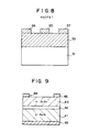
- FIG.8 shows a MESFET according to a third embodiment of the present invention wherein the composite semiconductor material of FIG.3 is used for the channel layer, similarly to the HEMT of FIG.7.
- the MESFET is constructed on a semi-insulating GaAs substrate 31 corresponding to the substrate 21, and a channel layer 33, doped to the n-type and having the composite semiconductor structure of FIG.3, is provided on the substrate 31.
- a gate electrode 35 On the upper major surface of the channel layer 33, there is provided a gate electrode 35 in Schottky contact therewith, and ohmic electrodes 36 and 37 are provided as the source and the drain of the device at both sides of the gate electrode 35. In this device, too, one obtains a very fast transport of carriers through the channel layer without substantial scattering by the optical phonons.
- FIG.9 shows an LED according to a fourth embodiment that uses a direct transition of carriers occurring in the composite semiconductor structure of FIG.3 for producing optical radiation.
- the device is constructed on a p-type GaAs crystal layer 41, and a layer 42 corresponding to the composite semiconductor structure of FIG.3 is formed epitaxially on the layer 41 with a total thickness of 100 ⁇ .
- a layer 42 corresponding to the composite semiconductor structure of FIG.3 is formed epitaxially on the layer 41 with a total thickness of 100 ⁇ .
- an ohmic electrode 45 is provided to cover the lower major surface of the GaAs layer 41.
- a ring-shaped ohmic electrode 46 formed with a passage or window 44 of optical beam such that the optical beam can exit freely from the device.
- a forward bias voltage is applied across the electrodes 46 and 45 for injecting electrons and holes into the layer 42 of the composite semiconductor structure, and optical radiation is formed as a result of recombination of the electrons and holes.
- the recombination of carriers occurs not only in the GaAs layer 12 but also in the Ge layer 12 because of the quantum well structure as explained previously.
- the composite semiconductor structure of the present invention is not only useful in the high-speed semiconductor devices but also in the optical semiconductor devices.
- the structure of the first through fourth embodiments of the present invention can be fabricated easily by the MBE process or MOCVD process with excellent control of the layer thickness.
Landscapes
- Engineering & Computer Science (AREA)
- Chemical & Material Sciences (AREA)
- Nanotechnology (AREA)
- Physics & Mathematics (AREA)
- Mathematical Physics (AREA)
- Theoretical Computer Science (AREA)
- Crystallography & Structural Chemistry (AREA)
- Junction Field-Effect Transistors (AREA)
- Recrystallisation Techniques (AREA)
- Led Devices (AREA)
Applications Claiming Priority (2)
| Application Number | Priority Date | Filing Date | Title |
|---|---|---|---|
| JP195325/91 | 1991-08-05 | ||
| JP19532591A JPH0541355A (ja) | 1991-08-05 | 1991-08-05 | 変調半導体材料およびそれを用いた半導体装置 |
Publications (3)
| Publication Number | Publication Date |
|---|---|
| EP0526870A2 true EP0526870A2 (de) | 1993-02-10 |
| EP0526870A3 EP0526870A3 (en) | 1993-08-25 |
| EP0526870B1 EP0526870B1 (de) | 1998-11-04 |
Family
ID=16339292
Family Applications (1)
| Application Number | Title | Priority Date | Filing Date |
|---|---|---|---|
| EP92113232A Expired - Lifetime EP0526870B1 (de) | 1991-08-05 | 1992-08-03 | Verbundshalbleiterstruktur zur Verminderung der Trägerssteuerung durch optischen Phononen und Halbleiteranordnung, die eine solche Verbundshalbleiterstruktur enthält |
Country Status (3)
| Country | Link |
|---|---|
| US (1) | US5336901A (de) |
| EP (1) | EP0526870B1 (de) |
| JP (1) | JPH0541355A (de) |
Families Citing this family (4)
| Publication number | Priority date | Publication date | Assignee | Title |
|---|---|---|---|---|
| EP0266425B1 (de) * | 1986-04-01 | 1991-10-30 | IIDA, Katumi | Wasserkläranlage vom lüftungstyp |
| US5917195A (en) * | 1995-02-17 | 1999-06-29 | B.A. Painter, Iii | Phonon resonator and method for its production |
| AUPR083300A0 (en) * | 2000-10-17 | 2000-11-09 | Silex Systems Limited | An isotope structure formed in an indriect band gap semiconductor material |
| KR101996424B1 (ko) * | 2017-04-24 | 2019-07-04 | 아주대학교산학협력단 | 레이저 다이오드 및 그 제조 방법 |
Family Cites Families (5)
| Publication number | Priority date | Publication date | Assignee | Title |
|---|---|---|---|---|
| US4163237A (en) * | 1978-04-24 | 1979-07-31 | Bell Telephone Laboratories, Incorporated | High mobility multilayered heterojunction devices employing modulated doping |
| US4261771A (en) * | 1979-10-31 | 1981-04-14 | Bell Telephone Laboratories, Incorporated | Method of fabricating periodic monolayer semiconductor structures by molecular beam epitaxy |
| JPS6028268A (ja) * | 1983-07-26 | 1985-02-13 | Agency Of Ind Science & Technol | 半導体装置 |
| JPS60175450A (ja) * | 1984-02-22 | 1985-09-09 | Toshiba Corp | ヘテロ接合バイポ−ラ半導体素子 |
| JPH03218078A (ja) * | 1990-01-23 | 1991-09-25 | Sanyo Electric Co Ltd | 光センサ |
-
1991
- 1991-08-05 JP JP19532591A patent/JPH0541355A/ja not_active Withdrawn
-
1992
- 1992-08-03 EP EP92113232A patent/EP0526870B1/de not_active Expired - Lifetime
-
1994
- 1994-03-07 US US08/206,220 patent/US5336901A/en not_active Expired - Lifetime
Also Published As
| Publication number | Publication date |
|---|---|
| US5336901A (en) | 1994-08-09 |
| EP0526870A3 (en) | 1993-08-25 |
| JPH0541355A (ja) | 1993-02-19 |
| EP0526870B1 (de) | 1998-11-04 |
Similar Documents
| Publication | Publication Date | Title |
|---|---|---|
| JP3194941B2 (ja) | 半導体装置 | |
| US5079774A (en) | Polarization-tunable optoelectronic devices | |
| US5373186A (en) | Bipolar transistor with monoatomic base layer between emitter and collector layers | |
| US5436468A (en) | Ordered mixed crystal semiconductor superlattice device | |
| JP2537852B2 (ja) | 高移動度半導体装置 | |
| US4721983A (en) | Three terminal tunneling device | |
| KR20020068365A (ko) | 분극 유발 전하를 줄인 고효율 광방출기 | |
| EP0594442A2 (de) | Schottky-Übergang Anordnung | |
| US5272712A (en) | Semiconductor laser device | |
| JPH07120790B2 (ja) | 半導体装置 | |
| US4733282A (en) | One-dimensional quantum pipeline type carrier path semiconductor devices | |
| EP0243953A2 (de) | Zusammengesetztes Halbleiterbauelement | |
| EP0610893B1 (de) | Diodenlaser | |
| Schulman | Effects of compositional grading on GaAs–Ga1− x Al x As interface and quantum well electronic structure | |
| US5473173A (en) | Quantum well structure having differentially strained quantum well layers | |
| US5336901A (en) | Composite semiconductor structure for reducing scattering of carriers by optical phonons and a semiconductor device that uses such a composite semiconductor structure | |
| US5132746A (en) | Biaxial-stress barrier shifts in pseudomorphic tunnel devices | |
| US6222205B1 (en) | Layered semiconductor structure for lateral current spreading, and light emitting diode including such a current spreading structure | |
| EP0136108B1 (de) | Halbleiteranordnung mit Heteroübergang | |
| US5280182A (en) | Resonant tunneling transistor with barrier layers | |
| US5289013A (en) | Phonon and charge carrier separation in quantum wells | |
| US5523585A (en) | Semiconductor device having a superlattice structure | |
| US5216260A (en) | Optically bistable semiconductor device with pairs of monoatomic layers separated by intrinsic layers | |
| JP2796113B2 (ja) | 半導体装置 | |
| US6479842B1 (en) | Field effect transistor with a quantum-wave interference layer |
Legal Events
| Date | Code | Title | Description |
|---|---|---|---|
| PUAI | Public reference made under article 153(3) epc to a published international application that has entered the european phase |
Free format text: ORIGINAL CODE: 0009012 |
|
| AK | Designated contracting states |
Kind code of ref document: A2 Designated state(s): DE FR GB |
|
| PUAL | Search report despatched |
Free format text: ORIGINAL CODE: 0009013 |
|
| AK | Designated contracting states |
Kind code of ref document: A3 Designated state(s): DE FR GB |
|
| 17P | Request for examination filed |
Effective date: 19940218 |
|
| 17Q | First examination report despatched |
Effective date: 19960125 |
|
| GRAG | Despatch of communication of intention to grant |
Free format text: ORIGINAL CODE: EPIDOS AGRA |
|
| GRAG | Despatch of communication of intention to grant |
Free format text: ORIGINAL CODE: EPIDOS AGRA |
|
| GRAH | Despatch of communication of intention to grant a patent |
Free format text: ORIGINAL CODE: EPIDOS IGRA |
|
| RBV | Designated contracting states (corrected) |
Designated state(s): FR |
|
| GRAH | Despatch of communication of intention to grant a patent |
Free format text: ORIGINAL CODE: EPIDOS IGRA |
|
| REG | Reference to a national code |
Ref country code: DE Ref legal event code: 8566 |
|
| GRAA | (expected) grant |
Free format text: ORIGINAL CODE: 0009210 |
|
| AK | Designated contracting states |
Kind code of ref document: B1 Designated state(s): FR |
|
| ET | Fr: translation filed | ||
| PLBE | No opposition filed within time limit |
Free format text: ORIGINAL CODE: 0009261 |
|
| STAA | Information on the status of an ep patent application or granted ep patent |
Free format text: STATUS: NO OPPOSITION FILED WITHIN TIME LIMIT |
|
| 26N | No opposition filed | ||
| PGFP | Annual fee paid to national office [announced via postgrant information from national office to epo] |
Ref country code: FR Payment date: 20050809 Year of fee payment: 14 |
|
| REG | Reference to a national code |
Ref country code: FR Ref legal event code: ST Effective date: 20070430 |
|
| PG25 | Lapsed in a contracting state [announced via postgrant information from national office to epo] |
Ref country code: FR Free format text: LAPSE BECAUSE OF NON-PAYMENT OF DUE FEES Effective date: 20060831 |