EP0526930A1 - Gepufferte Prozessorschnittstelle für Mehrprozessorsystemen - Google Patents
Gepufferte Prozessorschnittstelle für Mehrprozessorsystemen Download PDFInfo
- Publication number
- EP0526930A1 EP0526930A1 EP92202127A EP92202127A EP0526930A1 EP 0526930 A1 EP0526930 A1 EP 0526930A1 EP 92202127 A EP92202127 A EP 92202127A EP 92202127 A EP92202127 A EP 92202127A EP 0526930 A1 EP0526930 A1 EP 0526930A1
- Authority
- EP
- European Patent Office
- Prior art keywords
- data
- address
- processor
- memory
- microprocessor
- Prior art date
- Legal status (The legal status is an assumption and is not a legal conclusion. Google has not performed a legal analysis and makes no representation as to the accuracy of the status listed.)
- Withdrawn
Links
Images




Classifications
-
- G—PHYSICS
- G06—COMPUTING OR CALCULATING; COUNTING
- G06F—ELECTRIC DIGITAL DATA PROCESSING
- G06F13/00—Interconnection of, or transfer of information or other signals between, memories, input/output devices or central processing units
- G06F13/38—Information transfer, e.g. on bus
- G06F13/42—Bus transfer protocol, e.g. handshake; Synchronisation
- G06F13/4204—Bus transfer protocol, e.g. handshake; Synchronisation on a parallel bus
- G06F13/4208—Bus transfer protocol, e.g. handshake; Synchronisation on a parallel bus being a system bus, e.g. VME bus, Futurebus, Multibus
- G06F13/4217—Bus transfer protocol, e.g. handshake; Synchronisation on a parallel bus being a system bus, e.g. VME bus, Futurebus, Multibus with synchronous protocol
-
- G—PHYSICS
- G06—COMPUTING OR CALCULATING; COUNTING
- G06F—ELECTRIC DIGITAL DATA PROCESSING
- G06F12/00—Accessing, addressing or allocating within memory systems or architectures
- G06F12/02—Addressing or allocation; Relocation
- G06F12/08—Addressing or allocation; Relocation in hierarchically structured memory systems, e.g. virtual memory systems
- G06F12/0802—Addressing of a memory level in which the access to the desired data or data block requires associative addressing means, e.g. caches
- G06F12/0806—Multiuser, multiprocessor or multiprocessing cache systems
- G06F12/0815—Cache consistency protocols
- G06F12/0831—Cache consistency protocols using a bus scheme, e.g. with bus monitoring or watching means
- G06F12/0835—Cache consistency protocols using a bus scheme, e.g. with bus monitoring or watching means for main memory peripheral accesses (e.g. I/O or DMA)
-
- G—PHYSICS
- G06—COMPUTING OR CALCULATING; COUNTING
- G06F—ELECTRIC DIGITAL DATA PROCESSING
- G06F15/00—Digital computers in general; Data processing equipment in general
- G06F15/16—Combinations of two or more digital computers each having at least an arithmetic unit, a program unit and a register, e.g. for a simultaneous processing of several programs
- G06F15/163—Interprocessor communication
- G06F15/17—Interprocessor communication using an input/output type connection, e.g. channel, I/O port
Definitions
- This invention relates generally to multiprocessor data processing systems and, in particular, to method and apparatus for interfacing each of the processors to common, or shared, system resources and also to local, or private, processor resources.
- System requirements needed to interact with and visualize large, time-dependent data sets include a large, high-bandwidth disk array to store the entire data set being processed, a high speed network to download a problem set, a large, high-speed memory to buffer all data required to process a single simulation time step, computational power that is adequate to manipulate, enhance, and visualize the data sets, and a real-time, high resolution visual display. Furthermore, it is important that these functions be provided within a highly programmable and flexible user environment.
- An important consideration in a multiprocessor system is the interfacing of each of the processors to common, or shared, system resources and also to local, or private, processor resources. As an example, it may be required to interface each processor to a global bus having a system memory coupled thereto, while also coupling each processor to a private memory.
- Bus interface unit for distributing the control of data transfers within single instruction stream, multiple data stream processors.
- Bus interface units 13, 14, 15 are each connected between local memories (18, 19, 20), respectively, and a main bus 10 having a main memory 16 connected thereto through a bus interface unit 12.
- control channel interface for interfacing a processor to a time division multiplexed (TDM) bus.
- TDM time division multiplexed
- Each CCI is polled by a master processor to determine if the CCI has information to send.
- a CCI may buffer information until it can dispose of the information after being polled.
- the MPIF includes a dual ported RAM which can function as a FIFO, under the control of one processor, or as a shared memory.
- microprocessor-controlled circuit for interconnecting at least two very high speed integrated circuit chips having digital inputs and outputs.
- the circuit includes a local data bus, a microprocessor and associated memory, and a plurality of functional interface units.
- One functional interface unit is connected between the microprocessor and a local memory bus.
- each processor of a multiprocessor system including both computational and I/O processors, with an interface unit for coupling the processor to a private and to a shared memory, the interface unit further including control circuitry controlling the operation of a one line cache, external to the processor, that buffers read and write data passing between the processor and the shared memory.
- the invention teaches interface circuitry for coupling to a microprocessor device.
- the interface circuitry includes an input for coupling to the microprocessor device for receiving address signal lines and control signal lines generated by the microprocessor device.
- the interface further includes an address decoder, responsive to the received address signal lines, for determining if a microprocessor-generated memory access is directed to a private memory, accessible only by the microprocessor device, or to a shared memory that is accessible by a plurality of microprocessor devices. Responsive to the address decoder, the interface circuitry provides first address signal lines and first control signal lines to the private memory in response to the microprocessor device generating a memory access to the private memory means. Also responsive to the address decoder, the interface circuitry provides second address signal lines and second control signal lines for coupling to the shared memory in response to the microprocessor device generating a memory access to the shared memory.
- the interface circuitry of the invention is particularly useful in a multiprocessor embodiment wherein a plurality of processor devices share a common memory over a high speed system or global bus.
- the interface circuitry provides both a local (private) memory interface and a shared memory interface for an associated processor.
- the interface circuitry also provides a number of additional functions including interrupt control, inter-processor interrupt capability, and direct memory access functions for transferring data between the shared memory and the private memory.
- the interface circuitry also provides a number of miscellaneous functions such as programmable timer/counters, processor reset logic, and private memory refresh control.
- the interface circuitry also includes circuitry for interfacing to a serial diagnostic bus.
- the interface circuitry furthermore manages external read and write buffers that are interposed between a processor node data bus and the global data bus.
- the read and write buffers function in a manner similar to a one line cache and serve to reduce the bandwidth requirements of the global bus.
- FIG. 1 there is illustrated a multiprocessor system that includes a serial diagnostic bus and controller that is constructed and operated in accordance with the invention. Specifically, there are illustrated components of a Scientific Visualization System (SVS) 10.
- SVS 10 Scientific Visualization System
- a purpose of the SVS 10 is to process, manipulate, and visualize complex data sets at interactive speeds, although the use of the system 10 is not limited to only this one important application.
- the use of the processor interface of the invention is not restricted to only this particular system. That is, the processor interface as taught by the invention may be employed to advantage in a number of different types of multiprocessor systems.
- the SVS 10 includes several major components.
- a first component is a server 12 embodied within a data processing system that provides large-scale computational power, high-speed memory, and intelligent I/O processors, all of which are interconnected by a high speed global bus.
- the terms global bus, shared bus, and common interconnect are used interchangeably herein.
- a second component is a console processor 14 embodied in, by example, a RISC System/6000 (RS/6000) workstation manufactured by the International Business Machines Corporation (RISC System/6000 is a Trademark of the International Business Machines Corporation).
- the console 14 provides network access from remote workstations (not shown) and interfaces with the serial diagnostic controller of the invention in a manner described below.
- a third component is a Frame buffer 16 that includes, by example, an RS/6000 workstation that provides console functions therefor.
- the frame buffer 16 includes interface and image buffering hardware 16a attached via an ANSI standard High Performance Parallel Interface (HIPPI) interface for providing real-time display capability to high-resolution displays 18.
- HIPPI High Performance Parallel Interface
- a further component of the system 10 is a disk array 20.
- the disk array 20 may be embodied within a storage system having 21 GByte capacity with 55 MByte/second transfer rate via a HIPPI interface.
- Server 12 is comprised of a plurality of individual processors 22a organized as four processors (P1-P4) per printed circuit card 22.
- the server 12 may include up to eight cards for a total of 32 processors.
- Each processor card 22 includes a universal bus interface (UBIF) 34 for coupling a Local Processor Card (LPC) bus 32 to an SVS global bus 24.
- LPC Local Processor Card
- SVS global bus 24 Also coupled to the SVS global bus 24 are a plurality of Global Memory cards 26, a plurality of I/O processor cards 28, and an interface 30 to the RS/6000 console 14.
- each processor card 22 includes up to four processor nodes each having a microprocessor 22a.
- each microprocessor 22a is an i860-type device, specifically an 80860 microprocessor device manufactured by Intel Corporation (i860 is a Trademark of the Intel Corporation).
- a local node bus 23 comprised of a local node data bus 23a, a local node address bus 23b, and a local node control bus 23c, is a local node memory 22b providing, in this embodiment, 16 megabytes (MB) of storage.
- MB 16 megabytes
- Each processor node also includes, in accordance with the invention, a Processor Buffered Interface (PBIF) 22c, which incorporates an interface to the LPC bus 32. Additionally, each processor node includes an interface 22d (seen in Fig. 2) to a serial bus (S).
- PBIF Processor Buffered Interface
- S serial bus
- one of the processor cards 22 is capable of a peak performance of 160 million instructions per second (MIPS), or 320 million single precision floating point operations per second (MFLOPS).
- MIPS 160 million instructions per second
- MFLOPS single precision floating point operations per second
- a fully configured system of eight processor cards 22 provides a peak performance approaching 1.28 billion instructions per second (BIPS) or 2.56 GFLOPS, assuming 40 MHz operation.
- each of the Global Memory cards 26 is configured with either 128 MB or 256 MB of random access memory with error correction logic.
- the server 12 may include up to four Global Memory cards 26.
- Each of the Global Memory cards 26 provides a data bandwidth of 640 MB/second in a manner that reduces a memory access latency seen by each processor in the system 10. This is accomplished by partitioning the Global Memory on each memory card 26 into four memory banks (BO-B3), each of which is capable of independently performing block read cycles, page mode read or write cycles and random read or write cycles.
- a Global Memory Card (GMC) bus 26a enables each of the banks (BO-B3) to operate independently, while utilizing common global bus resources.
- the I/O processor cards 28 each include a processor node 28a, similar to the processor card 22, plus two HIPPI receivers 28b, and two HIPPI transmitters 28C. Each IOP 28 provides four HIPPI interfaces, each of which is capable of operation at a transfer rate of 100 MB/second. Each IOP 28 includes a dedicated processor node 28a, such as is found on the processor card 22, having a microprocessor coupled to 16MB of local memory. Two receiver channels 28b and two transmitter channels 28c are provided on each IOP 28. The channels may operate independently to deliver 100 Mbytes/second each, or in a paired manner to deliver 200 Mbytes/second.
- the HIPPI interfaces are employed to support high speed disk arrays, provide real-time images to HIPPI-attached frame buffers, and realize high speed communication with external devices, such as supercomputers.
- the Console interface 30 is partitioned into two cards, one which is found within the server 12 and one which resides in the console 14.
- the link between the two card allows access to the SVS server global memory and serial bus, which in turn allows access to each processor's local memory and PBIF.
- the system 10 also includes an Arbiter 36 that is coupled to the Global Bus 24 and which operates to arbitrate requests for the Global Bus between the processors 22, the memory 26, console interface 30, and the I/O processors 28.
- Arbiter 36 that is coupled to the Global Bus 24 and which operates to arbitrate requests for the Global Bus between the processors 22, the memory 26, console interface 30, and the I/O processors 28.
- the Global Bus 24 is implemented with Emitter Coupled Logic (ECL) technology for interconnecting these various components and providing a 1.28 GB/sec transfer rate.
- ECL Emitter Coupled Logic
- Appendix A describes the various Global Bus 24 signal lines.
- Major signal groups of the Global Bus 24 include a 32-bit address bus (ABUS) 24a, a 256-bit data bus (DBUS) 24b, and a control bus.
- Each SVS 10 server 12 supports up to 12 master devices (i.e. processor cards 22, I/O processor cards 28, or Interface card 30), and up to four memory cards 26.
- One configuration includes an Interface card 30, eight processor cards 22 (or 32 processors), four Global Memory cards 26 each with 256 MBytes of storage for a total of 1024 MB of high speed memory, and one I/O processor 28 to support the high speed disk array 20, receive data from a HIPPI source, and distribute image data to HIPPI attached frame buffers 16.
- the console 14 provides a user interface to the SVS 10 as well as support for standard I/O devices.
- each component card of the system 10 includes one of the UBIFs 34.
- the UBIF 34 presents a shared, synchronous, decoupled interface to the Global Bus 24, provides local arbitration on the LPC bus 32 or GMC bus 26a, and performs all necessary handshaking and retry sequencing with the Global bus 24.
- the UBIF 34 provides bidirectional, pipelined buffering to support up to four local master devices, such as processors 22a, or up to four slave devices, such as the memory banks B1-B4.
- the UBIF 34 supports data bus widths between eight bits and 256 bits and provides a peak data transfer rate of 1.28 Gbytes/second between the Local Bus 32 and the Global Bus 24, assuming 40 MHz bus operation (25 nanosecond bus cycle).
- the PBIF 22c functions as an interface and a control device for the associated computational processor 22a or I/O processor 28a.
- the PBIF 22c provides all of the required logic, with the exception of tranceivers and memory, to interface a high performance microprocessor to a high performance multi-processor system.
- the PBIF 22c functions in an identical manner with each of the I/O processors 28a.
- the PBIF 22c architecture is implemented as a set of discrete data registers together with an Application Specific Integrated Circuit (ASIC).
- ASIC Application Specific Integrated Circuit
- Each PBIF 22c provides control and address generation for up to 32 MBytes of local memory 22b.
- Each PBIF 22c provides control signals to an external 256-bit wide read and write buffer 22e to cache Global Memory 26 operations.
- Each PBIF 22c provides support for up to eight externally generated interrupts and eight internally generated interrupts.
- Each PBIF 22c provides support for an inter-processor interrupt mechanism whereby a processor in the system can interrupt any other processor (or group of processors).
- Each PBIF 22c provides a means of transferring data at high speed between the Global Memory 26 and the associated Local Memory 22b using direct memory access cycles.
- Each PBIF 22c incorporates a Control and Status Register (CSR), two programmable timer/counters, logic to reset the associated processor 22a or 28a, and other functions, as will be described.
- CSR Control and Status Register
- Each PBIF 22c includes circuitry that works in concert with a serial diagnostic bus, as described in European patent application 92 109 675.6 (IBM Docket No. YO 991 042).
- FIG. 4 A block diagram of the PBIF 22c, showing the partitioning of the device into these functional blocks, is shown in Fig. 4.
- PBIF 22c includes a plurality of state machines, including a Control/Status Register (CSR) state machine 78, a local memory state machine 52, and a global memory state machine 54. These three state machines have inputs connected to the control and address signal lines of the attached processor 22a or 28a.
- the global memory state machine 54 receives an input from a DMA controller 56 and an interprocessor communication (IPC) register 58.
- the local memory state machine 52 generates local memory address and control signal lines that are coupled to the local memory 22b for controlling accesses thereto.
- the global memory state machine 54 generates global memory address and control signal lines that are coupled via the local processor bus 32 and the UBIF 34 to the global bus 24.
- the global memory state machine 54 generates global memory address and control signals in response to the local processor 22a or 28a or in response to the operation of the DMA controller 56 or the IPC register 58.
- the DMA controller 56 further includes a source address register 56a, a destination address register 56b, and a length/blocksize register 56c. These registers are loaded by the attached processor for controlling DMA operations.
- the source address register 56a is initially loaded with the memory address from which data is to be read
- the destination address register 56b is initially loaded with the address to which the data is to be stored
- the length/blocksize register 56c is initially loaded with a value representing a number of data units that are to be transferred during a DMA operation.
- PBIF 22c also includes a timer/counter register 60a and a time stamp register 60b.
- the PBIF 22c also includes a control status register 62, the operation of which is described in further detail below.
- the PBIF 22c includes a block of interrupt-related registers. These include an interrupt register 64a which latches incoming interrupts and then, in turn, interrupts the processor 22a, as appropriate.
- the PBIF 22c further includes an interrupt mask register 64b, a clear interrupt register 64c, and a memory fault address register 64d.
- a refresh register 66 is provided for controlling the refresh timing parameters for the local memory 22b DRAMs.
- the aforementioned IPC register 58 has an associated send interrupt register 68.
- the serial diagnostic controller 70 is described in the aforementioned European patent application 92 109 675.6 (IBM Docket No. YO 991 042).
- the aforementioned registers 56 through 68 are all bidirectionally coupled to the local processor through a data multiplexer 72 such that the local processor is enabled to store information within and read information from these registers.
- Fig. 5 shows in greater detail the construction of the PBIF 22c and also shows in greater detail the input and output signal lines. Specifically, the outputs of the local memory state machine 52 and the global memory state machine 54 are shown in greater detail.
- the block diagram of Fig. 5 also shows several other state machines including a reset state machine 74, a LED state machine 76, and the CSR state machine 78.
- the serial diagnostic controller 70 can be seen to include a serial state machine 70a, an address register 70b and a data register 70c all of which are connected in series and have an output connected to a serial out signal line that is threaded through each of the PBIFs within the system 10.
- Fig. 6 shows in greater detail the interconnection, within a local processor node, of the PBIF 22c to the local processor 22a (or 28a), the local memory 22b, the global memory interface 22e, and the local bus 32.
- the local memory 22b is partitioned into 8 Mbyte banks and also includes a parity memory section for storing parity memory information associated with each of the memory banks.
- a set of eight registered transceivers 22f is employed for bidirectionally interfacing the memory banks and parity memory to the local node 64-bit data bus 23a.
- a set of eight transceivers 22g bidirectionally couple the local node data bus 23a to the read and write buffers of the global memory interface 22e.
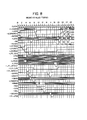
- Fig. 7 is a timing diagram showing the global memory 26 write timing that is generated by the global memory state machine 54. Signal names shown in Fig. 7 correspond to the signal designations of Fig. 5 and are described in Appendix B. Global Bus 24 signal designators are described in Appendix A. LPC bus 32 signal designators are described in Appendix C.
- Fig. 8 is a timing diagram that depicts global memory 26 read timing that is generated by the global memory state machine 54. It should be noted that the global memory read and write timing includes local memory 22b signal generation, as provided by the local memory state machine 52, and local bus 32 signal generation.
- Figs. 9 and 10 show in greater detail the operation of the IPC portion of the PBIF 22c. Specifically, Fig. 9 shows the IPC register 58 format and the coupling of the IPC register 58 to the local bus 32 and to the global bus 24. Fig. 10 shows in greater detail the IPC logic 80, particularly an IPC cycle detection logic block 80a and an IPC processor selection logic block 80b.
- the PBIF 22c provides all of the required logic, with the exception of tranceivers and memory, to interface a high performance microprocessor to a high performance multi- processor system. These functions are now described in greater detail below.
- the local memory 22b interface includes an address multiplexer 82 that provides both the address multiplexing for row and column addresses, and also the local memory state machine 52 that generates control signals required to interface to up to 32 MBytes of local memory 22b. This capability is based on the number of multiplexed address lines which this particular implementation of the PBIF 22c generates. Other embodiments may provide access to more or less than 32 MBytes of local memory.
- the PBIF 22c also provides a programmable refresh rate for the local memory 22b.
- the refresh register 66 is written with a divisor that is applied to the system clock. The resulting divided clock is used to periodically generate refresh cycles. Any refresh request is queued until all currently executing memory cycles are complete. The pending refresh request then has priority over any new cycles requested by the processor 22a. Local memory 22b refresh occurs unhindered if the processor 22a is accessing another range in memory (such as Global Memory 26).
- the processor 22a for this embodiment of the invention, includes an internal 8 KB data cache and a 4 KB instruction cache having cache lines that are 256-bits in width, and an external data bus that is 64 bits in width.
- the width of the internal cache line coincides with the width of the Global Data Bus (DBUS 24b), although the width of the processor 22a data bus is a factor of four less than that of DBUS 24b.
- the two external 256-bit registers 22e provide data bus width matching, and also provide an external, one line, level two cache for the processor 22a.
- the address is decoded within the PBIF 22c by address decode block 84 and the relevant request lines to the UBIF 34 (which controls the Global Bus 24) are generated.
- the PBIF 22c drives the address onto the LPC bus 32, along with any necessary control lines.
- the PBIF 22c then "snoops" the local bus 32, waiting for the Global Memory 26 data to be returned.
- the PBIF 22c When data is returned to an identified processor from the Global Memory 26, the PBIF 22c generates control signals to latch the returned data into the external read buffer 86, and then enables the appropriate word (64-bits) back to the identified processor 22a via the local node data bus 23a. If the processor 22a follows the first request with another request to a 64-bit word, which is also encached within the 256-bit read buffer 86, the second 64-bit word is returned to the processor 22a from the read buffer 86 with minimal latency, and without utilizing any bus bandwidth on either of the shared busses (LPC 32 and GB 24).
- the shared busses LPC 32 and GB 24
- the global memory state machine 54 is optimized to support cache reloads, where consecutive words are loaded into the processor 22a. After the initial latency for the first Global Memory 26 read, all subsequent words are returned in two bus cycles.
- Various address comparison functions are performed within the PBIF 22c with registers 90a and 90b and comparators 92a, 92b, 92c, and 94.
- Registers 90a and 90b maintain a record of the addresses of words that are currently stored in the external buffers 22e. If an out-of-sequence read is requested from the buffer 86 (i.e. the least significant 64-bits followed by the most significant 64-bits), an additional cycle is allowed for bus turnaround, and the read requires three cycles to complete. Reference is again made to the timing diagrams for Global Memory 26 reads (Fig. 8) and writes (Fig. 7).
- the contents of the read buffer 86 are invalidated if the processor 22a requests a word which is not currently cached, or if the currently cached word is detected as being written on the Global Bus 24.
- the PBIF 22c snoops all bus cycles on the Global Bus 24 to determine if a write takes place to a location in Global Memory 26 which is currently encached within the associated read buffer 86. This snooping function is accomplished with comparator 94.
- some conditions result in an invalidation of the read buffer 86. For example, a read from the processor 22a, with N10_LOCK active, invalidates the current contents of the read buffer 86, and the data is instead fetched from GM 26. However, this condition may be disabled via a Control Status Register 62 bit.
- Another signal line (LPC_NOCACHE) on the local bus 32 enables external devices to signal that they are returning non-cacheable data. Also, if a processor 22a writes the same address as is currently cached for reads, the read buffer 86 is invalidated. Furthermore, as a fail safe mechanism, the read buffer 86 may be automatically invalidated by the PBIF 22c after 256 reads of the same encached data, without a read buffer 86 reload from Global Memory 26. This feature is controlled by a bit in the CSR 62. The combination of these features ensures that any data stored within the read buffer 86 remains consistent with the copy stored within Global Memory 26.
- the write buffer 88 operates in a similar fashion.
- the processor 22a writes a word to a Global Memory 26 location, it is cached in the write buffer 88. Any further writes within the same 256-bits are stored within the write buffer 88.
- the write buffer 88 circuitry includes a register 88b for storing processor 22a byte enables, and updates these buffered write enables as appropriate. If the processor 22a writes to a location that is not currently cached in the write buffer 88 the contents of the write buffer 88 are flushed out to Global Memory 26, with the PBIF 22c generating the appropriate control signals, and the newly written word replaces the old within the write buffer 88.
- a software-controllable mode enables the write buffer 88 to be written out to Global Memory 26 after all 32 bytes have been written by the associated processor 22a.
- the write buffer 88 is also flushed if the processor 22a issues a locked write to Global Memory 26.
- a locked write is a special type of write cycle which the processor 22a may execute. During locked memory cycles, only the processor which initiated the lock is allowed to alter the data which it locked. This ensures consistency in multiprocessor systems, where many processors may attempt to share the same data.
- the processor 22a indicates a locked cycle by enabling a special output pin (N10_LOCK) during the cycle. If a locked write is requested to Global Memory 26, this condition first flushes the present contents of the write buffer 88, so as to maintain order, and then writes the locked word without buffering it. This operation is similar to that previously described for locked reads.
- a read of a Global Memory 26 address which is currently buffered in the write buffer 88 causes the write buffer 88 to be flushed before the read request is issued. This ensures that if the copy of the data in the write buffer 88 is more current than that contained within the Global Memory 26, that the most current version is returned to the requesting processor.
- the PBIF 22c also implements timeout mechanisms for all shared bus accesses.
- the 32-bit local bus address corresponds to a 256-bit data address
- the most significant five address bits are programmable, via a segment register in the PBIF 22c, to allow 128 Gbytes of Global Memory 26 to be addressed.
- the PBIF 22c supports up to eight external, level-sensitive interrupts and eight internally generated interrupts.
- the interrupts are individually maskable through the interrupt mask register 64b, and individually clearable through the clear interrupt register 64c. Any active, non-masked interrupts are OR'd together and passed through to the single interrupt input pin of the processor 22a.
- the Memory Fault Address Register (MFAR) 64d stores the last three addresses accessed by the processor 22a, and in the event of a parity, ECC or bus error interrupt, enables the failing address to be read.
- Timer/Counter Interrupt This interrupt is set after the timer/counter 60a is initialized to a starting value and subsequently decrements to zero.
- This interrupt is set when the PBIF 22c receives a request from the processor 22a to an address which is not mapped.
- This interrupt is set when the PBIF 22c receives an interrupt packet over the serial diagnostic interface bus.
- Buserror Interrupt This interrupt is set when the PBIF 22c times out while attempting to access the local bus 32.
- This interrupt is set at the completion of a DMA operation.
- two pins (+ LPC - ECCERR--I and + LPC - ERRTYPE--I) are implemented on the PBIF 22c and are used as interrupt inputs for indicating ECC errors returned with data read from Global Memory 26.
- the PBIF 22c contains two registers 58 and 68 which support the sending of inter-processor interrupts.
- the IPC register 58 is differentiated into a Processor Select Mask register 58a and a GSI register 58b.
- the Processor Select Mask register 58a (Fig. 9) defines a destination mask and has a width of 32-bits, with each bit being associated with one of the system 10 processors. This enables a processor to send an interrupt to any one processor, or group of processors, within the system.
- An additional four bits stored within the GSI register 58b select a destination system unit, or the type of processor (computation or I/O).
- the second register is the Send Interrupt Register 68 (Fig. 4) which controls the dispatch of the interrupt.
- a processor may also interrupt itself via this mechanism.
- the IPC interrupt is performed as a special local bus 32 cycle.
- the PBIF 22c sends an IPC interrupt message as a special read cycle that is differentiated from a normal read cycle by means of an extra pin on the local bus, LPC_ATYPE.
- This special local bus read cycle is passed through to the Global Bus 24 by the associated UBIF 34, and is decoded (Fig. 10) by the UBIF on any card which has its specific identifier set in the destination field.
- the LPC bus address lines, LPC_A(31:0) are used to convey the 32- bit processor 22a mask, and the length field, LPC_LEN(3:0), is used to convey the additional descriptor information.
- the UBIF 34 on any card which decodes a valid bit in the destination field generates the signal IPCINTR(3:0) to interrupt the relevant processor(s).
- the PBIF 22c supports Block DMA between the Global Memory 26 and the associated local memory 22b by means of the source address register 56a, the destination address register 56b, and the length/blocksize register 56c.
- the Global bus 24 supports block data transfers, both the size of the blocks to be transferred and the number of blocks are specified. Returned data blocks are stored in the UBIF 34 until requested by the PBIF 22c. In a presently preferred UBIF 34 implementation, eight 256-bit words may be stored per processor 22a. From the UBIF 34 the DMA data is written into the Global Memory 26 read buffer 86, before being transferred to the local memory 22b data transceivers 22f and 22g 64-bits at a time.
- the DMA controller writes the local memory 22b at its full bandwidth, accommodates local memory 22b refresh during DMA operations, and also requests ahead on the local bus 32 for the next 256-bit word from Global Memory 26 so as to minimize any latency.
- the PBIF 22c holds the processor 22a off the local bus 32 whilst DMA operations are taking place, and enables transfers to be achieved at up to 80 MBytes/second, assuming no contention on the Global Bus 24.
- An end of DMA interrupt signals completion of the operation.
- the Control and Status Register (CSR) 62 controls numerous functions within the PBIF 22c, including setting a mode for read buffer 86 and write buffer 88 operation.
- the CSR 62 is a 32-bit register containing some bits which are read/write (r/w), some bits that are read-only (r/o), and other bits that are write-only (w/o).
- the CSR 62 bit definitions follow.
- a (r/w) bit enables the write buffer 88 autoflush mode. When set to one, this bit allows the PBIF 22c write buffer 88 to be automatically flushed out to Global Memory 26 when all 32 bytes have been written by the local processor 22a. When cleared to zero (default), the PBIF 22c write buffer 88 is flushed only (a) when the associated processor's global write address is outside of the active 32-byte write block, (b) when the processor 22a issues a read to an address contained in the active 32-byte write block, or (c) when the processor 22a issues a LOCK write cycle to Global Memory 26.
- a (r/w) bit enables read buffer 86 auto-invalidate mode. When set to one, this bit enables the PBIF 22c read buffer 86 to be invalidated after 256 consecutive processor 22a reads to the same 32-byte Global Memory 26 address.
- a (r/w) bit enables the read buffer 86. When set to one, this bit enables buffered reads from the PBIF 22c read data buffer, which holds up to 32 consecutive bytes aligned on 32-byte global address boundaries. When cleared to zero (default), the PBIF 22c reflects every processor 22a read to the global address space on the LPC bus and Global Bus 24. That is, all reads come from GM 26, and not from date previously stored in the read buffer 86.
- a (r/w) bit enables the write buffer 88. When set to one, this bit enables processor writes to be buffered within the write data buffer 88, which holds up to 32 consecutive bytes aligned on 32-byte global address boundaries. When cleared to zero (default), the PBIF 22c reflects every processor 22a write to the global address space on the LPC bus 32 and Global Bus 24, via the write buffer 88.
- a (w/o) bit resets a fault condition.
- the current fault condition is cleared and the memory fault address register 64d resumes latching Memory 26 addresses issued by the processor 22a.
- the memory fault address register 64d reflects the physical address of the most recent memory reference which caused the error condition.
- a (r/w) bit functions as a timer mode select.
- the interrupt timer 60a continuously decrements from an initial value, generates a processor 22a interrupt, and resets to its initial value.
- the timer 60a decrements from its initial value, generates a processor 22a interrupt, and then ceases operation until reloaded by the processor 22a.
- Two (r/o) bits are used as local memory size bits and indicate the size of local memory 22b on the processor 22a. With the two bits set to 00, 01, 10, or 11 they indicate 8, 16, 32 or 8 Mbytes, respectively, for the size of the local memory 22b.
- Eight (r/o) bits are processor identifier bits.
- the resulting 8-bit code reflects the unique hardware identifier of the attached processor 22a, which is used to tag processor read requests to the Global Bus 24.
- the 8-bit code is composed of a 2-bit UNITID, which identifies SVS 10 system units in a closely coupled, multi-SVS configuration, a 4-bit SLOTID, which identifies the backplane slot to which the processor card 22 is connected, and a 2-bit LOC - PROCID, which uniquely identifies the processor 22a number on the processor card 22.
- a (r/w) bit functions as a processor boot bit. This bit controls whether the processor 22a will boot in 8- bit mode or in 64-bit mode following a reset. The default is the 64-bit mode.
- a (r/w) bit specifies a Request (REQ) to Grant (GNT) timeout period. This bit controls if the PBIF 22c will timeout if an LPC REQ or LPC WREQ does not receive an LPC GNT within some predetermined number of cycles. The occurrence of a timeout with this bit enabled sets the BUSERR interrupt to the processor 22a.
- Another (r/w) bit is a Read reply timeout bit and controls whether the PBIF will timeout if it is waiting for data to be returned on the LPC bus 32 and does not receive an LPC_DCYCLE signal with an ID_MATCH within some predetermined number of cycles. The occurrence of a timeout with this bit enabled sets the BUSERR interrupt to the processor 22a.
- a (r/w) bit is a PTB Enable bit and, if active, determines if the Global Memory state machine 54 responds to the processor + N10_PTB--I signal line. If this signal line is active, and PTB is enabled, and the PBIF 22c does not cache (read or write) the processor 22a global memory request.
- a (r/w) bit functions as an ECC Enable bit. If this bit is inactive the PBIF 22c ignores all incoming ECC errors. If this bit is active ECC errors generate interrupts and invalidate the Global Memory 26 read buffer 86 as appropriate.
- a further interface provides control from the processor 22a, via the LED state machine 76, of four intelligent alpha-numeric displays (not shown).
- a serial interface between the PBIF 22c and the displays is implemented to reduce pin count. Writing of any one display element is accomplished by writing a Display register 90 (Fig. 5) with an ASCII character code and an identifier of the display to receive the character.
- the reset state machine 74 ensures that the processor 22a is held in reset until all registers in the PBIF 22c are correctly initialized (after power on, for instance). These registers may be initially loaded via the Serial Diagnostics Interface bus from a system console (Host 14).
- the PBIF 22c implements a serial diagnostic bus, which enables a host computer to perform numerous control functions, or to access any part of memory which the local processor 22a can access.
- a serial bus master is enabled to read or write global or local memory or any of the registers within the PBIF 22c.
- the serial bus master can halt, and subsequently continue, any processor, reboot a processor or a processor node, or send an interrupt to an individual processor or a group of processors.
- the serial bus thus "mimics" the operation of a processor and in this manner is capable of performing any operation which a processor can perform.
- PBIF 22c GM 26 interface The operation of the PBIF 22c GM 26 interface is described with reference to the GM 26 state machine 54, illustrated in Fig. 11, and in reference to the GB 24 timing diagrams, illustrated in Figs. 7 and 8.
- Data path performance to the GM 26 is improved, as stated above, by the provision of the 256-bit read buffer 86 and the 256-bit write buffer 88, both of which may be turned selectively enabled or disabled through bits in CSR 62.
- Buffers 86 and 88 provide bus-width matching between the processor 22a and the LPC bus 32, and also provide posting capability for writes, and increased throughput on pipelined reads.
- the contents of the read buffer 86 are invalidated under the following circumstances: (a) a write on the GB 24 to the current read address (snoop match); (b) a GM 26 write request to the current read address; (c) a read to an address different than the current read address; (d) a volatile read (as indicated by + NOCACHE on the LPC bus 32); (e) a read from the processor 22a with the PTB bit set (and enabled in the CSR 62); and (f) autoflush after 256 reads from the same 32-byte address.
- the read buffer 86 is not set as a result of a read request which fails to complete (e.g. timeout), or as a result of a read request which returns bad data (e.g. GM 26 parity or ECC error).
- the contents of the write buffer 88 are flushed to the GM 26 under one of four conditions: (a) a condition indicated by the CSR 62 mode bit is met; (b) the performance of a locked write request, which flushes any data currently in the write buffer 88, and then performs the locked write to GM 26; and (c) a read to the address which is currently active in the write buffer 88. In this case the write buffer 88 is flushed before the read request is issued.
- write flush modes There are two write flush modes which may be set under software control. If the above described CSR 62 bit is enabled, then the default mode for operation is to flush the write buffer 88 contents whenever the write buffer 88 contains valid data, and the processor 22a writes to a different address in the GM 26. In the second mode, the contents of the write buffer 88 are flushed whenever all 32 bytes of the 256 bit word have been written, as indicated by the byte enables.
- a register within the GM 26 state machine 54 latches the byte enables whenever a GM 26 write occurs, and when all 32 bits are set, generates a signal -BYTES_FULL, which causes a state machine 54 transition. This register is reset whenever the contents of the write buffer 88 are flushed.
- the GM 26 state machine 54 also allows requests to go out onto the LPC bus 32 for other local devices. In this case, the GM 26 operation is initiated by an 10 address decode rather than a GM 26 address decode by address decoder 84.
- the LPC bus 32 interface also provides the address buffers 90a and 90b.
- Buffer 90a stores the address of the current read buffer 86, and is enabled onto the LPC bus 32 during a read cycle.
- Buffer 90b stores the current write address. Two buffers are required so that if the processor 22a writes a 64-bit word, and then proceeds to read in a cache line before writing the rest of the 256 bits (and flushing the write buffer 88), the correct write address is driven to the LPC bus 32 during the write cycle.
- Buffers 90a and 90b are implemented as 27-bit registers to hold the GM 26 read buffer 86 and write buffer 88 addresses. These buffers are latched under the control of the GM 26 state machine 54. It is noted that the 27 most significant bits of the GB 24 address bus are driven on the 27 least significant bits of the LPC address bus. Just as the GB 24 address drives 29 address bits (three are ignored because of 64-bit addressing) so the PBIF 22c drives 27 bits (five are ignored because of 256-bit addressing). The top five bits of the LPC address field are set, on all GM 26 (or IOSEL) operations, to a value which is stored in a segment register (SEGREG) 90c. This register is initialized to zero by a reset, and is subsequently written, if required, so as to address a larger GM 26 address space.
- SEGREG segment register
- the latched addresses are used as input to a number of comparators.
- Comparators 92a and 92b compare the buffered read and write addresses, respectively, with the processor 22a address (bits 28-2). Thus, if the read buffer 86 contains the currently active read address, and the processor 22a issues a read request to the same page such that the address bits match, then comparator 92a asserts the signal R_MATCH, and the state machine 54 responds accordingly.
- a signal W_MATCH is similarly generated by comparator 92b.
- the third comparator 92c compares the latched read and write addresses. This comparison is performed at the same time as the previous two comparisons.
- a fourth comparator 94 compares the read address with the snoop address from the LPC bus 32.
- a fifth comparator (not shown) compares two bits of MID from the LPC bus 32 with hardwired ID to the PBIFc.
- Register 88a exists external to the PBIF 22c to drive the LPC bus 32, and exists also as a "shadow" register within the PBIF 22c. Eight-bit portions of register 88a are individually loaded, and the register 88a is cleared with one signal. The stored byte enables, each of which corresponds to one byte in the write buffer 88, are combined to generate the signal LPC RMW. This line is driven with the LPC bus 32 address on writes and is low if all of the byte enables are set.
- the state machine 54 begins in the idle state (SO).
- a GM 26 write is requested by the processor 22a in the same manner as a local memory write, with the appropriate address decode signalling that this write is to be posted to the GB 24.
- S1 is entered and READY goes low to the processor 22a, indicating that the data has been written.
- the data is latched into the write buffer 88, and the state machine 54 proceeds to state S21.
- Also latched in state S1 is the read buffer 86 address.
- the write buffer 88 flag is set active. From state S21, state S22 is entered.
- the state machine 54 From S0, if the processor 22a issues another write request, and the W - MATCH signal indicates that this write is in the same 256-bit block as the address stored in write buffer 88, then the state machine 54 enters state S2, the data is latched, READY is returned to the processor 22a, and the write address is latched.
- a write request to any GM 26 location when the write buffer 88 enable bit is not set, also causes the write to occur in state S2 (rather than S1).
- the state machine 54 branches to state S21, unless either the write buffer 88 is disabled, or all 32-bytes of data have been written, in which case a branch is made to S3 to initiate the LPC bus 32 write. In the case of branching to S21, the same procedure is followed as has just been described.
- an output enable to LPC bus 32 transceivers goes active, and is conditioned by the appearance of a Grant from a LPC bus 32 arbiter.
- a GRANT signal from the LPC arbiter is asserted, the address is driven onto the LPC bus 32, and at the end of this cycle, the state machine 54 enters state S4.
- the LPC LOCK line is driven active whenever the LPC ADDR is driven active, and the request is a result of a processor 22a request with N10_LOCK active.
- the intention is to set the lock bit for all write buffer 88 flushes initiated either by an SO to S7 transition, or by an S6 to S7 transition (but only if these were caused by locked writes, not PTB writes), or by an SO to S2 transition which is caused by a locked write with the write buffer 88 disabled.
- the lock bit is set by a locked read request. This causes an SO to S8 transition, so that the data is read from GM 26 and not from the read buffer 86, as would occur on an SO to S19 transition. In addition, for a locked read, the data is not cached by read buffer 86.
- LPC_LEN(3:0) The four LPC bus 32 length lines (LPC_LEN(3:0)) are driven, with the address, to zero for all "normal" GM 26 requests.
- S4 the output enables for the data transceivers are active, and the data is driven out onto the LPC bus 32 in this cycle.
- the address is also driven onto the bus for one additional cycle (a two cycle active period).
- state machine 54 transitions to state S5, where the data is enabled onto the LPC bus 32 for a second cycle, and the write buffer 88 valid flag is disabled. Following S5, the state machine 54 waits in state S6 until either an ACK or a NAK is received from the associated UBIF 34.
- the state machine 54 branches back to state S3, and a further write request is issued. If an ACK is received, the state machine 54 may branch to one of three states, depending on the condition that caused the write buffer 88 flush.
- the state machine 54 branches to state S1, where the data and address for the new write are latched into the appropriate ones of the buffers 90b and 88, and READY is returned to the processor 22a.
- the write buffer 88 active flag is also set.
- the state machine 54 branches back to the idle state S0, after transferring the contents of the write buffer 88 out onto the LPC bus 32.
- state machine 54 branches to state S7, where the address and data for the locked write are latched into their respective write buffers.
- the write buffer 88 active flag is set, and READY is returned to the processor 22a.
- a branch is made to state S3 to flush the locked write out to the LPC bus 32.
- a branch to state S7, directly from the idle state S0, may occur if a locked write request is received and the write buffer 88 is either inactive, or has an address that matches the requested locked write address. In this case the address and data are latched, and the state machine 54 branches to S3 to flush the data. At this point, the write to GM 26 is complete, as far as the processor 22a is concerned.
- a processor 22a read from GM 26 is now described. It is assumed that the read buffer 86 is initially empty.
- the state machine 54 branches to state S8. In this state an LPC read request is signalled, and the read address is clocked into the read address buffer 90a. From S8 state S9 is entered. The state machine 54 loops at S9, while maintaining the LPC bus 32 read request asserted, until a GNT from the LPC bus 32 arbiter is received. When the GNT is received, the read address is driven during this cycle onto the LPC bus 32, and also in the following cycle.
- state machine 54 proceeds to state S10 on receipt of a GNT.
- state S10 the read address is driven for a second cycle to the LPC bus 32, and a signal line becomes active indicating that the state machine 54 is waiting to receive data.
- state S20 then S11 is entered, where the state machine 54 loops until either an ACK or a NAK is received. If NAK is received, a transition is made back to state S9 to resend the request. If ACK is received, state S12 is entered.
- state S12 signal Next Address (NA) is asserted to the processor 22a, indicating that it may place a new address on the processor address bus 23b, and the state machine 54 then proceeds to state S13, where it loops until that the requested data from GM 26 is available on the LPC bus 32. While in state S13 the read buffer 86 latches data from the LPC bus 32 every cycle until the correct data appears and state S13 is exited. If the processor 22a has, in the meantime, placed a new address on address bus 23b the address is held by processor 22a until the next acknowledgement from the state machine 54. If this next address is, for example, a read request to local memory 22b, this read does not take place until the GM 26 has finished returning the previously requested read data.
- N Next Address
- State S200 adds an additional wait state to the write, as the processor 22a delays asserting data by one clock on a write cycle following a read cycle. If, however, there is instead a read cycle pending to the same 256 bit word of data, as indicated by R MATCH from comparater 92a, the state machine 54 branches to state S16. If any other type of request is pending, state machine 54 returns to state S0, and the read buffer 86 valid signal is invalidated.
- a signal is asserted that indicates to the processor 22a that it may send another request onto the processor bus 23.
- a signal is also asserted setting up data for return to the processor 22a during S17.
- a decode of which bank of the read buffer 86 should be enabled is accomplished by decoding the least two significant address bits of the LPC bus 32 address bus.
- S17 the data for the current read from the read buffer 86 is returned to the processor 22a.
- the state machine 54 transitions to state S18 and enables the next data word to the processor, if appropriate. If this is the case, a read match occurs and the state machine 54 loops back to state S17, where the next word is returned to the processor 22a.
- the state machine 54 returns to S0, and may restart a new Global Memory read or write cycle, if required. It is noted that the state machine 54 here "preempts" the processor 22a, and assumes that it will read consecutive addresses from the read buffer 86, when in pipeline mode. If, at the end of S18, there is a read request to a location in the read buffer 86, but not to an address contiguous with the address of the data just returned (i.e. the processor 22a has skipped a data word), a branch is made to state S19, where the correct word is enabled onto the processor 22a data bus, before a branch to state S17 is made to return the data to the processor 22a.
- This extra state ensures enough time for the read buffer 86 to drive the data bus 23a before the processor 22a latches the data.
- This tight loop (S17-S18-S17 etc.) enables the read buffer 86 to return data to the processor 22a every other cycle so as to accommodate the processor's maximum bandwidth.
- the above described architecture and implementation provides a powerful and flexible interface capability for a microprocessor-based multiprocessor systems.
- Some of the functions implemented by the PBIF 22c are useful in any type of multiprocessor system, such as the internal timer logic.
- the Global Memory 26 interface provides increased performance from the relatively high latency Global Memory 26 subsystem.
- certain functions are optimized around the characteristics of the selected microprocessor device.
- variations in certain of the features may be made to accommodate the characteristics of the attached processor.
- variations in the interrupt structure may be made so as to accommodate a processor having more than one interrupt input.
- variations in the state machine 54 may be required to accommodate different processors, such as the addition or deletion of certain states that provide processor- specific timing delays, etc.
Landscapes
- Engineering & Computer Science (AREA)
- Theoretical Computer Science (AREA)
- Physics & Mathematics (AREA)
- General Engineering & Computer Science (AREA)
- General Physics & Mathematics (AREA)
- Computer Hardware Design (AREA)
- Software Systems (AREA)
- Multi Processors (AREA)
Applications Claiming Priority (2)
| Application Number | Priority Date | Filing Date | Title |
|---|---|---|---|
| US07/733,517 US5410654A (en) | 1991-07-22 | 1991-07-22 | Interface with address decoder for selectively generating first and second address and control signals respectively in response to received address and control signals |
| US733517 | 1991-07-22 |
Publications (1)
| Publication Number | Publication Date |
|---|---|
| EP0526930A1 true EP0526930A1 (de) | 1993-02-10 |
Family
ID=24947951
Family Applications (1)
| Application Number | Title | Priority Date | Filing Date |
|---|---|---|---|
| EP92202127A Withdrawn EP0526930A1 (de) | 1991-07-22 | 1992-07-11 | Gepufferte Prozessorschnittstelle für Mehrprozessorsystemen |
Country Status (3)
| Country | Link |
|---|---|
| US (1) | US5410654A (de) |
| EP (1) | EP0526930A1 (de) |
| JP (1) | JPH05189383A (de) |
Cited By (3)
| Publication number | Priority date | Publication date | Assignee | Title |
|---|---|---|---|---|
| EP0580961A1 (de) * | 1992-07-17 | 1994-02-02 | International Business Machines Corporation | Gepufferte Prozessorschnittstelle für Mehrprozessorsysteme |
| EP0752666A3 (de) * | 1995-07-06 | 2004-04-28 | Sun Microsystems, Inc. | Verfahren und Vorrichtung zur Beschleunigung von Sklave-Anforderungen in einem paketvermittelten Computersystem |
| US20050027914A1 (en) * | 2003-07-31 | 2005-02-03 | Per Hammalund | Inter-processor interrupts |
Families Citing this family (44)
| Publication number | Priority date | Publication date | Assignee | Title |
|---|---|---|---|---|
| US5822601A (en) * | 1989-12-29 | 1998-10-13 | Packard Bell Nec | Apparatus to allow a CPU to control the relocation of code blocks for other CPUs |
| ES2139583T3 (es) * | 1992-08-19 | 2000-02-16 | Siemens Nixdorf Inf Syst | Sistema multiprocesador con memorias cache. |
| US5745791A (en) * | 1992-09-16 | 1998-04-28 | Intel Corporation | System for interfacing first and second components having different data path width by generating first and second component address to read data into buffer |
| GB2271204B (en) * | 1992-10-01 | 1996-01-03 | Digital Equipment Int | Digital system memory access |
| JP3524110B2 (ja) * | 1992-11-06 | 2004-05-10 | 株式会社ルネサステクノロジ | マイクロコンピュータシステム |
| US5749092A (en) * | 1993-03-18 | 1998-05-05 | Intel Corporation | Method and apparatus for using a direct memory access unit and a data cache unit in a microprocessor |
| US6116768A (en) * | 1993-11-30 | 2000-09-12 | Texas Instruments Incorporated | Three input arithmetic logic unit with barrel rotator |
| US5577204A (en) * | 1993-12-15 | 1996-11-19 | Convex Computer Corporation | Parallel processing computer system interconnections utilizing unidirectional communication links with separate request and response lines for direct communication or using a crossbar switching device |
| DE19501674A1 (de) * | 1994-02-03 | 1995-08-10 | Tektronix Inc | Verwaltung der Datenübertragung zwischen Prozessoren |
| WO1996011440A1 (en) * | 1994-10-06 | 1996-04-18 | Virc, Inc. | Shared memory system |
| US5615127A (en) * | 1994-11-30 | 1997-03-25 | International Business Machines Corporation | Parallel execution of a complex task partitioned into a plurality of entities |
| JP3339262B2 (ja) * | 1995-01-12 | 2002-10-28 | 三菱電機株式会社 | ミシンの制御装置及びその制御方法 |
| EP0723230B1 (de) * | 1995-01-23 | 2002-05-22 | Compaq Computer Corporation | Verteilter Datencachespeicher für Multiprozessorsystem mit Cachespeicher |
| WO1996030831A1 (en) * | 1995-03-31 | 1996-10-03 | Intel Corporation | Memory testing in a multiple processor computer system |
| US5909571A (en) * | 1995-05-01 | 1999-06-01 | Apple Computer, Inc. | Clock distribution for processor and host cards |
| US5566304A (en) * | 1995-05-08 | 1996-10-15 | Apple Computer, Inc. | Method of dynamic selection between immediate and delayed read access acknowledgement |
| US5613071A (en) * | 1995-07-14 | 1997-03-18 | Intel Corporation | Method and apparatus for providing remote memory access in a distributed memory multiprocessor system |
| JP3739797B2 (ja) * | 1995-10-06 | 2006-01-25 | パトリオット サイエンティフィック コーポレイション | 縮小命令セット・コンピューター・マイクロプロセッサーの構造 |
| KR0170500B1 (ko) * | 1995-11-18 | 1999-03-30 | 양승택 | 멀티프로세서 시스템 |
| US5970510A (en) * | 1996-04-10 | 1999-10-19 | Northrop Grumman Corporation | Distributed memory addressing system |
| US6041379A (en) * | 1996-10-04 | 2000-03-21 | Northrop Grumman Corporation | Processor interface for a distributed memory addressing system |
| US5862135A (en) * | 1996-10-10 | 1999-01-19 | Lucent Technologies Inc. | Simplified interface to a time-division multiplexed communications medium |
| US5901326A (en) * | 1996-11-26 | 1999-05-04 | International Business Machines Corporation | Memory bus address snooper logic for determining memory activity without performing memory accesses |
| US6430640B1 (en) * | 1997-03-07 | 2002-08-06 | Virtual Resources Communications, Inc. | Self-arbitrating, self-granting resource access |
| US6332165B1 (en) * | 1997-09-05 | 2001-12-18 | Sun Microsystems, Inc. | Multiprocessor computer system employing a mechanism for routing communication traffic through a cluster node having a slice of memory directed for pass through transactions |
| US6173374B1 (en) * | 1998-02-11 | 2001-01-09 | Lsi Logic Corporation | System and method for peer-to-peer accelerated I/O shipping between host bus adapters in clustered computer network |
| US6141710A (en) * | 1998-12-15 | 2000-10-31 | Daimlerchrysler Corporation | Interfacing vehicle data bus to intelligent transportation system (ITS) data bus via a gateway module |
| DE19957594B4 (de) * | 1999-11-30 | 2004-08-26 | OCé PRINTING SYSTEMS GMBH | Verfahren zum Synchronisieren von threads eines Computerprogramms |
| WO2001048755A1 (en) * | 1999-12-28 | 2001-07-05 | Matsushita Electric Industrial Co., Ltd. | Recording apparatus, reproducing apparatus, data processing apparatus, recording/reproducing apparatus, and data transmitting apparatus |
| US7035966B2 (en) | 2001-08-30 | 2006-04-25 | Micron Technology, Inc. | Processing system with direct memory transfer |
| US7035753B2 (en) * | 2002-03-20 | 2006-04-25 | Infineon Technologies Ag | Method and apparatus for placing an integrated circuit into a default mode of operation |
| US20030229738A1 (en) * | 2002-06-05 | 2003-12-11 | Dactron | Controller interface |
| US7321958B2 (en) * | 2003-10-30 | 2008-01-22 | International Business Machines Corporation | System and method for sharing memory by heterogeneous processors |
| US7355562B2 (en) * | 2004-02-17 | 2008-04-08 | Thomas Schubert | Electronic interlocking graphics panel formed of modular interconnecting parts |
| CN1998037A (zh) * | 2004-02-17 | 2007-07-11 | 维斯托艾斯(澳大利亚)控股有限公司 | 由模块化互连部分构成的电子互锁图形面板 |
| KR100652376B1 (ko) * | 2004-07-29 | 2006-12-01 | 삼성전자주식회사 | 분리 연산 가능한 구조를 가지는 모듈러 곱셈기와 이를포함하는 암호화 시스템 |
| US7991940B2 (en) * | 2005-07-25 | 2011-08-02 | Surf Communication Solutions Ltd. | Communication processor board |
| JP2007164243A (ja) * | 2005-12-09 | 2007-06-28 | Fuji Xerox Co Ltd | コントロール装置および記憶装置の有効利用方法 |
| US7725680B1 (en) * | 2006-07-06 | 2010-05-25 | Marvell International Ltd. | Pipeline interposer |
| KR100894121B1 (ko) * | 2006-09-07 | 2009-04-20 | 비스토이스(오스트레일리아) 피티와이 리미티드 | 모듈러 상호 연결부로 형성된 전자적 연동 그래픽 패널 |
| US8818802B2 (en) | 2008-10-10 | 2014-08-26 | Spansion Llc | Real-time data pattern analysis system and method of operation thereof |
| WO2010042631A2 (en) * | 2008-10-10 | 2010-04-15 | Fastow Richard M | Real-time data pattern analysis system and method of operation thereof |
| WO2015153693A1 (en) * | 2014-03-31 | 2015-10-08 | Xockets IP, LLC | Interface, interface methods, and systems for operating memory bus attached computing elements |
| US10635827B2 (en) * | 2016-11-18 | 2020-04-28 | Raptor Engineering, LLC | Systems and methods for secure isolation of legacy computer peripherals |
Citations (7)
| Publication number | Priority date | Publication date | Assignee | Title |
|---|---|---|---|---|
| US4495575A (en) * | 1981-12-09 | 1985-01-22 | Tokyo Shibaura Denki Kabushiki Kaisha | Information processing apparatus for virtual storage control system |
| US4675811A (en) * | 1983-12-27 | 1987-06-23 | Hitachi, Ltd. | Multi-processor system with hierarchy buffer storages |
| EP0244540A2 (de) * | 1986-05-05 | 1987-11-11 | Silicon Graphics, Inc. | Gerät zur Pufferung von Schreibanforderungen |
| EP0392657A1 (de) * | 1989-04-07 | 1990-10-17 | Tektronix Inc. | Direktspeicherzugriff zwischen unterschiedlichen Bussystemen mit Cachespeicherübereinstimmung |
| EP0404128A2 (de) * | 1989-06-21 | 1990-12-27 | Hitachi, Ltd. | Mehrrechnersystem mit hierarchischem Cache-Speicher |
| GB2233480A (en) * | 1989-06-22 | 1991-01-09 | Int Computers Ltd | Multiprocessor data processing system |
| EP0418621A2 (de) * | 1989-09-19 | 1991-03-27 | Fujitsu Limited | Datenverarbeitungseinrichtung zur Kohärenzaufrechthaltung von gespeicherten Daten im Hauptspeicher, externem Cachespeicher und internem Cachespeicher |
Family Cites Families (27)
| Publication number | Priority date | Publication date | Assignee | Title |
|---|---|---|---|---|
| US3573855A (en) * | 1968-12-31 | 1971-04-06 | Texas Instruments Inc | Computer memory protection |
| US4080649A (en) * | 1976-12-16 | 1978-03-21 | Honeywell Information Systems Inc. | Balancing the utilization of I/O system processors |
| US4223380A (en) * | 1978-04-06 | 1980-09-16 | Ncr Corporation | Distributed multiprocessor communication system |
| US4481580A (en) * | 1979-11-19 | 1984-11-06 | Sperry Corporation | Distributed data transfer control for parallel processor architectures |
| US4484273A (en) * | 1982-09-03 | 1984-11-20 | Sequoia Systems, Inc. | Modular computer system |
| US4663706A (en) * | 1982-10-28 | 1987-05-05 | Tandem Computers Incorporated | Multiprocessor multisystem communications network |
| US4698753A (en) * | 1982-11-09 | 1987-10-06 | Texas Instruments Incorporated | Multiprocessor interface device |
| US4511969A (en) * | 1983-05-20 | 1985-04-16 | At&T Information Systems Inc. | Control channel interface circuit |
| JPS60258671A (ja) * | 1984-06-05 | 1985-12-20 | Nec Corp | プロセツサ |
| US4648034A (en) * | 1984-08-27 | 1987-03-03 | Zilog, Inc. | Busy signal interface between master and slave processors in a computer system |
| JPS61156338A (ja) * | 1984-12-27 | 1986-07-16 | Toshiba Corp | マルチプロセツサシステム |
| US4843540A (en) * | 1986-09-02 | 1989-06-27 | The Trustees Of Columbia University In The City Of New York | Parallel processing method |
| US5123101A (en) * | 1986-11-12 | 1992-06-16 | Xerox Corporation | Multiple address space mapping technique for shared memory wherein a processor operates a fault handling routine upon a translator miss |
| US5142628A (en) * | 1986-12-26 | 1992-08-25 | Hitachi, Ltd. | Microcomputer system for communication |
| JPS6437773A (en) * | 1987-08-01 | 1989-02-08 | Sony Corp | Track jump device of disk device |
| JPH0831061B2 (ja) * | 1987-07-24 | 1996-03-27 | 株式会社日立製作所 | バツフア制御方式 |
| US5134700A (en) * | 1987-09-18 | 1992-07-28 | General Instrument Corporation | Microcomputer with internal ram security during external program mode |
| IT1223142B (it) * | 1987-11-17 | 1990-09-12 | Honeywell Bull Spa | Sistema multiprocessore di elaborazione con multiplazione di dati globali |
| US4872133A (en) * | 1988-02-18 | 1989-10-03 | Motorola, Inc. | Floating-point systolic array including serial processors |
| IT1216085B (it) * | 1988-03-15 | 1990-02-22 | Honeywell Bull Spa | Apparato di selezione veloce di memoria locale. |
| US4912633A (en) * | 1988-10-24 | 1990-03-27 | Ncr Corporation | Hierarchical multiple bus computer architecture |
| IT1227360B (it) * | 1988-11-18 | 1991-04-08 | Honeywell Bull Spa | Sistema multiprocessore di elaborazione dati con replicazione di dati globali. |
| US5276850A (en) * | 1988-12-27 | 1994-01-04 | Kabushiki Kaisha Toshiba | Information processing apparatus with cache memory and a processor which generates a data block address and a plurality of data subblock addresses simultaneously |
| US4964033A (en) * | 1989-01-03 | 1990-10-16 | Honeywell Inc. | Microprocessor controlled interconnection apparatus for very high speed integrated circuits |
| JPH02293958A (ja) * | 1989-04-07 | 1990-12-05 | Tektronix Inc | インタフェース装置 |
| JPH02293953A (ja) * | 1989-05-08 | 1990-12-05 | Nec Corp | 特定システム情報取得方式 |
| US5226134A (en) * | 1990-10-01 | 1993-07-06 | International Business Machines Corp. | Data processing system including a memory controller for direct or interleave memory accessing |
-
1991
- 1991-07-22 US US07/733,517 patent/US5410654A/en not_active Expired - Fee Related
-
1992
- 1992-07-02 JP JP4175248A patent/JPH05189383A/ja active Pending
- 1992-07-11 EP EP92202127A patent/EP0526930A1/de not_active Withdrawn
Patent Citations (7)
| Publication number | Priority date | Publication date | Assignee | Title |
|---|---|---|---|---|
| US4495575A (en) * | 1981-12-09 | 1985-01-22 | Tokyo Shibaura Denki Kabushiki Kaisha | Information processing apparatus for virtual storage control system |
| US4675811A (en) * | 1983-12-27 | 1987-06-23 | Hitachi, Ltd. | Multi-processor system with hierarchy buffer storages |
| EP0244540A2 (de) * | 1986-05-05 | 1987-11-11 | Silicon Graphics, Inc. | Gerät zur Pufferung von Schreibanforderungen |
| EP0392657A1 (de) * | 1989-04-07 | 1990-10-17 | Tektronix Inc. | Direktspeicherzugriff zwischen unterschiedlichen Bussystemen mit Cachespeicherübereinstimmung |
| EP0404128A2 (de) * | 1989-06-21 | 1990-12-27 | Hitachi, Ltd. | Mehrrechnersystem mit hierarchischem Cache-Speicher |
| GB2233480A (en) * | 1989-06-22 | 1991-01-09 | Int Computers Ltd | Multiprocessor data processing system |
| EP0418621A2 (de) * | 1989-09-19 | 1991-03-27 | Fujitsu Limited | Datenverarbeitungseinrichtung zur Kohärenzaufrechthaltung von gespeicherten Daten im Hauptspeicher, externem Cachespeicher und internem Cachespeicher |
Cited By (6)
| Publication number | Priority date | Publication date | Assignee | Title |
|---|---|---|---|---|
| EP0580961A1 (de) * | 1992-07-17 | 1994-02-02 | International Business Machines Corporation | Gepufferte Prozessorschnittstelle für Mehrprozessorsysteme |
| US5485594A (en) * | 1992-07-17 | 1996-01-16 | International Business Machines Corporation | Apparatus and method using an atomic fetch and add for establishing temporary ownership of a common system resource in a multiprocessor data processing system |
| US5634034A (en) * | 1992-07-17 | 1997-05-27 | International Business Machines Corporation | Enhanced processor buffered interface for multiprocess systems |
| EP0752666A3 (de) * | 1995-07-06 | 2004-04-28 | Sun Microsystems, Inc. | Verfahren und Vorrichtung zur Beschleunigung von Sklave-Anforderungen in einem paketvermittelten Computersystem |
| US20050027914A1 (en) * | 2003-07-31 | 2005-02-03 | Per Hammalund | Inter-processor interrupts |
| US8984199B2 (en) * | 2003-07-31 | 2015-03-17 | Intel Corporation | Inter-processor interrupts |
Also Published As
| Publication number | Publication date |
|---|---|
| US5410654A (en) | 1995-04-25 |
| JPH05189383A (ja) | 1993-07-30 |
Similar Documents
| Publication | Publication Date | Title |
|---|---|---|
| EP0526930A1 (de) | Gepufferte Prozessorschnittstelle für Mehrprozessorsystemen | |
| US5564008A (en) | An enhanced processor buffered interface for multiprocessor systems | |
| KR920004402B1 (ko) | 디지탈 데이타 프로세서용 버스 인터페이스 회로 | |
| EP0524683A1 (de) | Wissenschaftliches Anzeigesystem | |
| US4622631A (en) | Data processing system having a data coherence solution | |
| KR920008430B1 (ko) | 처리 판독 메모리 장치 | |
| US5191649A (en) | Multiprocessor computer system with data bus and ordered and out-of-order split data transactions | |
| CA1300280C (en) | Central processor unit for digital data processing system including write buffer management mechanism | |
| US5271020A (en) | Bus stretching protocol for handling invalid data | |
| CA1300279C (en) | Central processor unit for digital data processing system including cache management mechanism | |
| US5091845A (en) | System for controlling the storage of information in a cache memory | |
| EP0379769B1 (de) | Schreib-Lese/Schreib-Weitergabe-Speichersubsystemzyklus | |
| US5119484A (en) | Selections between alternate control word and current instruction generated control word for alu in respond to alu output and current instruction | |
| US5226170A (en) | Interface between processor and special instruction processor in digital data processing system | |
| US6728258B1 (en) | Multi-processor system and its network | |
| US5590338A (en) | Combined multiprocessor interrupt controller and interprocessor communication mechanism | |
| KR920004401B1 (ko) | 디지탈 데이타 프로세싱 시스템내의 프로세서와 특수명령 프로세서간의 인터페이스 | |
| US5517671A (en) | System for designating a plurality of I/O devices to a plurality of I/O channels and connecting and buffering the plurality of I/O channels to a single system bus | |
| Tuazon et al. | Mark IIIfp hypercube concurrent processor architecture | |
| US5276892A (en) | Destination control logic for arithmetic and logic unit for digital data processor | |
| AU617514B2 (en) | Multiple processor/cache memory system and data transaction control therefor | |
| EP0302926B1 (de) | Schaltung zur steuersignalerzeugung für eine arithmetische logische einheit in einem digitalverarbeitungsgerät | |
| CA1300275C (en) | Destination control logic for arithmetic and logic unit for digital data processor | |
| JPH0210462A (ja) | コンピユータ装置におけるキヤツシユの首尾一貫性を強いる方法およびコンピユータ装置 | |
| WO1988006763A1 (en) | Central processor unit for digital data processing system including virtual to physical address translation circuit |
Legal Events
| Date | Code | Title | Description |
|---|---|---|---|
| PUAI | Public reference made under article 153(3) epc to a published international application that has entered the european phase |
Free format text: ORIGINAL CODE: 0009012 |
|
| AK | Designated contracting states |
Kind code of ref document: A1 Designated state(s): DE FR GB |
|
| 17P | Request for examination filed |
Effective date: 19930519 |
|
| 18W | Application withdrawn |
Withdrawal date: 19960820 |