EP0527660B1 - Digitaler Frequenzmodulator - Google Patents
Digitaler Frequenzmodulator Download PDFInfo
- Publication number
- EP0527660B1 EP0527660B1 EP92307468A EP92307468A EP0527660B1 EP 0527660 B1 EP0527660 B1 EP 0527660B1 EP 92307468 A EP92307468 A EP 92307468A EP 92307468 A EP92307468 A EP 92307468A EP 0527660 B1 EP0527660 B1 EP 0527660B1
- Authority
- EP
- European Patent Office
- Prior art keywords
- data
- output
- input
- multiplication
- modulator
- Prior art date
- Legal status (The legal status is an assumption and is not a legal conclusion. Google has not performed a legal analysis and makes no representation as to the accuracy of the status listed.)
- Expired - Lifetime
Links
Images

Classifications
-
- H—ELECTRICITY
- H03—ELECTRONIC CIRCUITRY
- H03C—MODULATION
- H03C3/00—Angle modulation
Definitions
- the present invention relates to a digital FM modulator and, more particularly, to a digital FM modulator used for transmitting digital data including a television signal and an audio signal with an FM modulation wave.
- a modulation index of a digitized modulation signal is designated by external multiplication data, and a center frequency is set by addition data.
- Fig. 2 shows an arrangement of the conventional digital FM modulator.
- a modulation signal input to a modulation signal input terminal 11 is digital/analog-converted by an A/D converter 1 and input to one terminal of a multiplier 2.
- Multiplication data 13 is input to the other input terminal of the multiplier 2 and multiplied by an output from the A/D converter 1, and the data is output from the multiplier 2 and input to one input terminal of an adder 3.
- Addition data 14 is input to the other input terminal of the adder 3 and added to an output from the multiplier 2, and the data is output from the adder 3 and input to a direct digital synthesizer (to be referred to as a DDS hereinafter) 4.
- the DDS 4 integrates data input to the DDS 4 every output period of a reference oscillator 5. The integrated data is used as a phase amount to obtain a sine wave from an output terminal 12.
- Fig. 3 shows the DDS 4.
- the DDS 4 includes an accumulator 40 and a ROM 43.
- the accumulator 40 includes an adder 41 using an output from the adder 3 as an input and a delay circuit 42 for delaying an output from the adder 41 to be fed back to the adder 41.
- the ROM 43 uses an output from the adder 41 as an address input.
- the adder 41 adds the output from the adder 3 to an output from the delay circuit 42 delayed for one period every sampling period and outputs the resultant value to the ROM 43 as an address signal. For example, when an output from the adder 3 is set to be N, a value obtained by accumulating N to the output data from the adder 3 is output as an f signal every sampling period.
- the ROM 43 stores Sine wave data at consecutive addresses starting from address 0 and is accessed in response to the address signal of the f signal output from the accumulator 40 so as to output the Sine wave data having an output frequency F.
- the DDS 4 is described in the above prior art.
- the DDS 4 is operated with reference to the output frequency of the reference oscillator 5, thereby obtaining a frequency proportional to the content of the output data from the adder 3. Therefore, an FM modulation wave can be obtained from the output terminal 12, and the maximum frequency deviation and center frequency of the FM modulation wave are set by the multiplication data 13 and the addition data 14, respectively.
- a digital FM modulator comprising A/D converting means for digitally coding an input modulation signal, multiplying means for multiplying an output from the A/D converting means and multiplication data input from an external circuit, adding means for adding output data from the multiplying means to addition data, a direct digital synthesizer for changing an oscillation frequency on the basis of output data from the adding means with respect to a reference frequency of a reference oscillator, and addition data output means for changing the addition data to prevent a center frequency from changing in accordance with the multiplication data, thereby outputting the addition data.
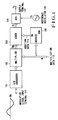
- Fig. 1 shows an embodiment of the present invention.
- reference numeral 101 denotes an A/D converter for A/D-converting a modulation signal input to a modulation signal input terminal 111; 102, a multiplier for multiplying an output from the A/D converter 101 and multiplication data 113; 103, an adder for adding output data D M from the multiplier 102 and addition data 114; 104, a DDS, having the same arrangement as that of Fig.
- ROM 106 for receiving output data D F from the adder 103 and an output f c from a reference oscillator 105 as inputs and outputting a sine wave of a frequency f0 to an output terminal 112; and 106, a ROM in which the plurality of addition data 114 corresponding to the multiplication data 113 to be changed are stored in advance.
- the ROM 106 outputs the addition data 114 which are read out by using the multiplication data 113 as an address input to the adder 103.
- Data D R stored in the ROM 106 is set as follows.
- a value of the multiplication data 113 for setting a maximum frequency deviation and a center value of modulation signal input data are represented by M and B0, respectively, and the center value B0 is input
- the number of bits of the output of an accumulator in the DDS 104, i.e., the accumulator 40 shown in Fig. 3 is represented by n
- the following data is required to output a desired output frequency f0:
- D F f 0 /f C ⁇ 2 n
- f c is the frequency of the reference oscillator 105.
- the data D R is calculated by the equation on the basis of the value M of the multiplication data 113 and stored in the ROM 106.
- a modulation signal input to the modulation signal input terminal 111 is input to the A/D converter 101 and analog/digital-converted to be input to one input terminal of the multiplier 102.
- the multiplication data 113 from an external circuit is input to the other input terminal of the multiplier 102 to be multiplied by an output from the A/D converter 101.
- the output data D M from the multiplier 102 is input to one input terminal of the adder 103.
- the multiplication data 113 is also input at an address of the ROM 106.
- the ROM 106 stores the addition data 114 corresponding to multiplication data in advance.
- the addition data 114 is stored such that the data D R in which a center frequency is not changed even when the multiplication data 113 is changed is calculated in advance.
- the output data D R from the ROM 106 is input to the other input terminal of the adder 103 as the addition data 114.
- the adder 103 adds the output data D M from the multiplier 102 to the addition data 114 and inputs the resultant value to the DDS 104.
- the DDS 104 is operated on the basis of the output frequency f c of the reference oscillator 105 and determines the frequency f0 in accordance with the output data D F from the adder 103. In this manner, an FM modulation wave can be obtained from the output terminal 112.
- a center frequency can be controlled in synchronization with the change in maximum frequency deviation. For this reason, the center frequency need not be set again.
Landscapes
- Digital Transmission Methods That Use Modulated Carrier Waves (AREA)
- Transmitters (AREA)
- Stabilization Of Oscillater, Synchronisation, Frequency Synthesizers (AREA)
Claims (4)
- Digitaler Frequenzmodulator mit:einem A/D-Wandler (101) zum digitalen Codieren eines Eingangsmodulationssignals;einer Multipliziereinrichtung (102) zum Multiplizieren der Ausgabe des A/D-Wandlers mit Multiplikationsdaten (113) als Eingabe von einem externen Schaltkreis;einer Addiereinrichtung (103) zum Addieren der Ausgabedaten (DM) der Multipliziereinrichtung zu Zusatzdaten (114); undeiner direkten Digital-Synthetisiereinrichtung (104) zum Ändern einer Oszillationsfrequenz (f₀) auf der Basis von Ausgabedaten (DF) der Addiereinrichtung bezüglich einer Bezugsfrequenz (fc) eines Bezugsoszillators (105);gekennzeichnet durcheine Zusatzdaten-Ausgabeeinrichtung (106) zum Ändern der Zusatzdaten, um zu verhindern, daß sich die Mittelfrequenz (B₀) entsprechend den Multiplikationsdaten ändert.
- Modulator nach Anspruch 1, wobei die Zusatzdaten-Ausgabeeinrichtung (106) ein erster Speicher ist, in dem Zusatzdaten entsprechend den Multiplikationsdaten gespeichert sind.
- Modulator nach Anspruch 2, wobei die Multiplikationsdaten (103) dem Speicher als Adreßdaten eingegeben werden und wobei die entsprechenden Zusatzdaten (114) ausgelesen und ausgegeben werden.
- Modulator nach Anspruch 1, wobei die direkte Digital-Synthetisiereinrichtung (104) einen Akkumulator (40) zum Berechnen eines kumulativen Wertes von Ausgabedaten der Addiereinrichtung (103) sowie einen zweiten Speicher (43) aufweist, in dem trigonometrische Funktionswerte in einer Adressenreihenfolge gespeichert sind und die trigonometrischen Funktionswerte in Intervallen ausgelesen werden, die durch Ausgaben des Akkumulators gekennzeichnet sind.
Applications Claiming Priority (2)
| Application Number | Priority Date | Filing Date | Title |
|---|---|---|---|
| JP204157/91 | 1991-08-14 | ||
| JP3204157A JPH0548338A (ja) | 1991-08-14 | 1991-08-14 | デイジタルfm変調器 |
Publications (2)
| Publication Number | Publication Date |
|---|---|
| EP0527660A1 EP0527660A1 (de) | 1993-02-17 |
| EP0527660B1 true EP0527660B1 (de) | 1996-02-28 |
Family
ID=16485783
Family Applications (1)
| Application Number | Title | Priority Date | Filing Date |
|---|---|---|---|
| EP92307468A Expired - Lifetime EP0527660B1 (de) | 1991-08-14 | 1992-08-14 | Digitaler Frequenzmodulator |
Country Status (3)
| Country | Link |
|---|---|
| US (1) | US5272454A (de) |
| EP (1) | EP0527660B1 (de) |
| JP (1) | JPH0548338A (de) |
Families Citing this family (10)
| Publication number | Priority date | Publication date | Assignee | Title |
|---|---|---|---|---|
| JPH0697738A (ja) * | 1992-09-10 | 1994-04-08 | Nec Corp | ディジタルfm変調器 |
| US5631920A (en) * | 1993-11-29 | 1997-05-20 | Lexmark International, Inc. | Spread spectrum clock generator |
| US5488627A (en) * | 1993-11-29 | 1996-01-30 | Lexmark International, Inc. | Spread spectrum clock generator and associated method |
| US6032028A (en) * | 1996-04-12 | 2000-02-29 | Continentral Electronics Corporation | Radio transmitter apparatus and method |
| DE59806211D1 (de) * | 1997-09-12 | 2002-12-12 | Siemens Ag | Schaltung zum erzeugen eines modulierten signals |
| US6163232A (en) * | 1998-08-20 | 2000-12-19 | Siemens Aktiengesellschaft | Frequency/phase modulator using a digital synthesis circuit in a phase locked loop |
| JP3621345B2 (ja) * | 2000-12-12 | 2005-02-16 | Necエレクトロニクス株式会社 | 複数のテレビジョン信号方式に対応可能な映像信号処理回路 |
| US7421043B2 (en) * | 2002-11-27 | 2008-09-02 | Lsi Corporation | Method and/or apparatus for stabilizing the frequency of digitally synthesized waveforms |
| US7224302B2 (en) * | 2005-08-23 | 2007-05-29 | Silicon Laboratories, Inc. | Integrated PM/FM modulator using direct digital frequency synthesis and method therefor |
| US7646258B2 (en) * | 2007-06-26 | 2010-01-12 | Karr Lawrence J | Digital FM transmitter with variable frequency complex digital IF |
Family Cites Families (3)
| Publication number | Priority date | Publication date | Assignee | Title |
|---|---|---|---|---|
| JPS62266903A (ja) * | 1986-05-15 | 1987-11-19 | Nec Home Electronics Ltd | デイジタルfm変調方式 |
| US4878035A (en) * | 1988-05-27 | 1989-10-31 | Wavetek Rf Products, Inc. | Hybrid frequency shift keying modulator and method |
| GB2234652A (en) * | 1989-08-01 | 1991-02-06 | Plessey Co Plc | Apparatus for generating digital wideband frequency modulated signals |
-
1991
- 1991-08-14 JP JP3204157A patent/JPH0548338A/ja active Pending
-
1992
- 1992-08-14 US US07/930,759 patent/US5272454A/en not_active Expired - Lifetime
- 1992-08-14 EP EP92307468A patent/EP0527660B1/de not_active Expired - Lifetime
Also Published As
| Publication number | Publication date |
|---|---|
| JPH0548338A (ja) | 1993-02-26 |
| US5272454A (en) | 1993-12-21 |
| EP0527660A1 (de) | 1993-02-17 |
Similar Documents
| Publication | Publication Date | Title |
|---|---|---|
| CA1229887A (en) | Temperature-compensated oscillation device | |
| US5563535A (en) | Direct digital frequency synthesizer using sigma-delta techniques | |
| EP0527660B1 (de) | Digitaler Frequenzmodulator | |
| US6198353B1 (en) | Phase locked loop having direct digital synthesizer dividers and improved phase detector | |
| US4974236A (en) | Arrangement for generating an SSB signal | |
| US4998072A (en) | High resolution direct digital synthesizer | |
| EP0479969B1 (de) | Synthesizer mit gebrochenem teilverhältnis für ein sprach-/daten-kommunikationssystem | |
| EP0419622B1 (de) | Frequenzsynthesizer mit gebrochenem teilverhältnis | |
| US4829463A (en) | Programmed time-changing coefficient digital filter | |
| US4752902A (en) | Digital frequency synthesizer | |
| US4684897A (en) | Frequency correction apparatus | |
| US5521534A (en) | Numerically controlled oscillator for generating a digitally represented sine wave output signal | |
| JP2002506603A (ja) | 多項式補間を用いたサンプルレート変換器 | |
| US4959616A (en) | Digital oscillation apparatus | |
| US5619535A (en) | Digital frequency synthesizer | |
| EP0459446B1 (de) | Digital gesteuerter Oszillator | |
| EP0378190B1 (de) | Digitale Phasenregelschleife | |
| EP0493057A1 (de) | Synthetisierer mit höherer Frequenzauflösung | |
| EP1645027B1 (de) | Verfahren und vorrichtung zur erzeugung beliebiger monozyklus-signalformen | |
| EP0599609A1 (de) | Frequenzsynthetisierer für ein Kommunikationssystem | |
| US8428213B2 (en) | Method for locking a synthesised output signal of a synthesised waveform synthesiser in a phase relationship | |
| JPH11289224A (ja) | 周波数シンセサイザ | |
| US5399998A (en) | Digital FM modulator | |
| JP3478901B2 (ja) | 周波数シンセサイザ装置 | |
| US20030151440A1 (en) | Digital clock generator |
Legal Events
| Date | Code | Title | Description |
|---|---|---|---|
| PUAI | Public reference made under article 153(3) epc to a published international application that has entered the european phase |
Free format text: ORIGINAL CODE: 0009012 |
|
| 17P | Request for examination filed |
Effective date: 19921125 |
|
| AK | Designated contracting states |
Kind code of ref document: A1 Designated state(s): FR GB |
|
| 17Q | First examination report despatched |
Effective date: 19950706 |
|
| GRAH | Despatch of communication of intention to grant a patent |
Free format text: ORIGINAL CODE: EPIDOS IGRA |
|
| GRAA | (expected) grant |
Free format text: ORIGINAL CODE: 0009210 |
|
| AK | Designated contracting states |
Kind code of ref document: B1 Designated state(s): FR GB |
|
| ET | Fr: translation filed | ||
| PLBE | No opposition filed within time limit |
Free format text: ORIGINAL CODE: 0009261 |
|
| STAA | Information on the status of an ep patent application or granted ep patent |
Free format text: STATUS: NO OPPOSITION FILED WITHIN TIME LIMIT |
|
| 26N | No opposition filed | ||
| REG | Reference to a national code |
Ref country code: GB Ref legal event code: IF02 |
|
| PGFP | Annual fee paid to national office [announced via postgrant information from national office to epo] |
Ref country code: FR Payment date: 20050809 Year of fee payment: 14 |
|
| PGFP | Annual fee paid to national office [announced via postgrant information from national office to epo] |
Ref country code: GB Payment date: 20050810 Year of fee payment: 14 |
|
| GBPC | Gb: european patent ceased through non-payment of renewal fee |
Effective date: 20060814 |
|
| REG | Reference to a national code |
Ref country code: FR Ref legal event code: ST Effective date: 20070430 |
|
| PG25 | Lapsed in a contracting state [announced via postgrant information from national office to epo] |
Ref country code: GB Free format text: LAPSE BECAUSE OF NON-PAYMENT OF DUE FEES Effective date: 20060814 |
|
| PG25 | Lapsed in a contracting state [announced via postgrant information from national office to epo] |
Ref country code: FR Free format text: LAPSE BECAUSE OF NON-PAYMENT OF DUE FEES Effective date: 20060831 |