EP0528060B1 - Procédé d'exécution d'operations d'entrée/sortie dans des systèmes de traitement de données - Google Patents
Procédé d'exécution d'operations d'entrée/sortie dans des systèmes de traitement de données Download PDFInfo
- Publication number
- EP0528060B1 EP0528060B1 EP91113605A EP91113605A EP0528060B1 EP 0528060 B1 EP0528060 B1 EP 0528060B1 EP 91113605 A EP91113605 A EP 91113605A EP 91113605 A EP91113605 A EP 91113605A EP 0528060 B1 EP0528060 B1 EP 0528060B1
- Authority
- EP
- European Patent Office
- Prior art keywords
- channel
- control
- input
- ctsys
- devices
- Prior art date
- Legal status (The legal status is an assumption and is not a legal conclusion. Google has not performed a legal analysis and makes no representation as to the accuracy of the status listed.)
- Expired - Lifetime
Links
Images


Classifications
-
- G—PHYSICS
- G06—COMPUTING OR CALCULATING; COUNTING
- G06F—ELECTRIC DIGITAL DATA PROCESSING
- G06F3/00—Input arrangements for transferring data to be processed into a form capable of being handled by the computer; Output arrangements for transferring data from processing unit to output unit, e.g. interface arrangements
- G06F3/06—Digital input from, or digital output to, record carriers, e.g. RAID, emulated record carriers or networked record carriers
- G06F3/0601—Interfaces specially adapted for storage systems
-
- G—PHYSICS
- G06—COMPUTING OR CALCULATING; COUNTING
- G06F—ELECTRIC DIGITAL DATA PROCESSING
- G06F13/00—Interconnection of, or transfer of information or other signals between, memories, input/output devices or central processing units
- G06F13/10—Program control for peripheral devices
- G06F13/12—Program control for peripheral devices using hardware independent of the central processor, e.g. channel or peripheral processor
- G06F13/122—Program control for peripheral devices using hardware independent of the central processor, e.g. channel or peripheral processor where hardware performs an I/O function other than control of data transfer
-
- G—PHYSICS
- G06—COMPUTING OR CALCULATING; COUNTING
- G06F—ELECTRIC DIGITAL DATA PROCESSING
- G06F3/00—Input arrangements for transferring data to be processed into a form capable of being handled by the computer; Output arrangements for transferring data from processing unit to output unit, e.g. interface arrangements
- G06F3/06—Digital input from, or digital output to, record carriers, e.g. RAID, emulated record carriers or networked record carriers
- G06F3/0601—Interfaces specially adapted for storage systems
- G06F3/0668—Interfaces specially adapted for storage systems adopting a particular infrastructure
- G06F3/0671—In-line storage system
- G06F3/0673—Single storage device
Definitions
- the invention relates to a method for performing input / output operations in data processing systems, in which an input / output operation is directed from an input / output processing unit to a peripheral input / output system consisting of rotating storage devices, in particular disk storage devices, according to the Preamble of claim 1.
- a multiplicity of input / output operations are carried out in data processing systems and are directed to a peripheral input / output system.
- An input / output operation is initiated by a processing unit and transferred to the input / output system by an input / output processing unit.
- the input / output system consists of rotating storage devices, e.g. Disk storage, there must be a continuous data path from a device to a channel system coupled to the input / output processing unit at the point in time at which the read / write heads of the device are located above the controlled location on the disk storage.
- channel-side data paths are arranged between the channel system and a control system connected to the storage devices, and device-side data paths in the control system.
- the data need not be transferred via the same path on which the input / output operation is transferred from the input / output processing unit to a storage device.
- the selected connection is released (disconnection) and later a continuous data path is established for the transmission of the data from the controlled storage device to the channel system consisting of several channels (reconnection) .
- the request for establishing such a return connection is signaled by the storage device, the device announcing itself some time before the point in time for reading or writing (lead) with a certain signal ( R otational P osition S ensing).
- interrupt signals are started, starting with the storage devices via the Control devices near the device and channel-side control devices of the control system up to the channels of the channel system, simultaneously generated on the parallel data paths. As soon as a complete data path is available for the transmission of the data, the remaining, partially established connections are broken up again.
- This principle of dynamic reconnection results in redundancy in all stages of the connection establishment and also requires the individual storage devices to be kept available for a longer period.
- the present invention has for its object to provide a method of the type mentioned, in which the time for performing input / output operations with rotating storage devices is shortened on average.
- control system defines individual device-side paths and a single channel-side path from the parallel data paths.
- Control and selection information indicate the alternatives of the different possible paths. By selecting certain paths, the provision of the interrupt signals on all paths can be avoided.
- the selection of only one path at the interface to the channels of the channel system has a particularly advantageous effect on the processing power, since only one channel is required to establish the return connection is.
- means are provided in the control system for temporarily storing the data to be transferred from the storage device or to be delivered to the storage device.
- control information identifies the channel-side data paths that can be selected for the connection, while the selection information specifies the device-side data paths provided for establishing the return connection in the control system.
- the switching on and off of a dynamic reverse connection at every stage of the connection establishment can thus be controlled in a simple manner using this information.
- the control and selection information is derived from commands that can be used to specify path groups with various possible data paths on the channel side for establishing the return connection.
- the selection information is formed by bit masks which individually determine the selection of the individual device-side data paths in the control system for each connected storage device.
- the use of a common control memory that can be read by all control devices for storing the selection information enables the paths for the connection to be selected directly at the interface to the storage devices.
- the Means for temporarily storing the data during a data transmission from or to the storage device are provided in each control device.
- control information is stored in a storage device provided for the administration entries of the individual storage devices.
- control information is stored in a communication memory common to all control devices.
- a free control device is determined on the basis of the stored control information and the one channel-side data path provided for the connection is selected.
- the means for temporarily storing the data to be taken from the storage device or to be transferred to the device are provided in all control devices.
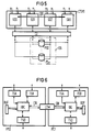
- FIG. 1 shows a data processing system in which peripheral input / output systems IOS can be accessed.
- Each input / output system IOS consists of a large number of rotating storage devices, for example disk storage PSO ... PSn, each with two device connection paths.
- the data processing system has a main memory MM, one or more processing units CPU and at least one input / output processing unit IOP. All units communicate with one another via a common line system SBUS, the input / output processing unit (s) IOP for carrying out input / output operations being additionally connected to an input / output line system IOBUS.
- a channel system CHSYS is also coupled to the IOBUS input / output line system.
- This channel system CHSYS which in the exemplary embodiment is limited to eight channels CH1 ... CH8, is connected to a downstream control system CTSYS via parallel, channel-side data paths.
- the system CTSYS forms the interface to the peripheral input / output systems IOS and thus serves as a controlling link between the channel system CHSYS coupled to the input / output processing unit IOP and the passive storage devices.
- the control system CTSYS is responsible for the control and control of the sequence of input / output operations and the production a reverse connection between one of the disk memories PSO ... PSn and one of the channels.
- the data to be delivered to the disk memory or to be taken over from the disk memory are transmitted past the input / output processing unit IOP via a direct access path DMA coupled to the channels CH1 ... CH8.
- control system CTSYS can select individual data paths from several parallel data paths on the device and channel side.
- the decision alternatives in the form of control and selection information for the individual release of the paths are stored in storage devices of the control system CTSYS.
- commands are provided, by means of which path groups are formed with different data paths on the channel side, which are suitable for establishing the return connection, and, if necessary, are resolved again.
- path group commands contain the control information from which the selection information is derived and then stored.
- An input / output operation triggered by a processing unit CPU for example a read or write job to a selected disk memory of an input / output system IOS, is carried out in two phases in real-time decoupling.
- operation and device-specific parameters e.g. device address, parameters for the positioning of the read / write heads of the selected device, addresses for the memory blocks, block lengths, etc.
- This data is transferred to the addressed disk storage via a free channel-side data path in the CHSYS channel system and a specified device-side data path in the CTSYS control system. Then the established connection is released (disconnection).
- the second phase is iniitiert itself from disk by these logs via its two-device connection paths with an interrupt signal (R P otational osition S ensing) in control system CTSYS.
- This signal notifies the readiness of the storage device for data transfer in good time before the point in time for reading or writing.
- a continuous return connection (reconnection) from the controlled device to the channel system CHSYS must be made available.
- the control system is used to establish the return connection
- CTSYS defined individual paths based on the control and selection information from the parallel data paths.
- An interruption signal arrives at the CHSYS channel system only via these defined data paths, with only one data path with the associated channel for the connection of the interruption signal to the input / output processing unit IOP being selected from the channel-side data paths provided for the dynamic reconnection by the path group commands.
- the selection of certain device-side data paths in the control system CTSYS and in particular the assignment of only one channel-side data path in the channel system CHSYS for the establishment of the return connection makes a parallel provision of interrupt signals on all data paths superfluous.
- the control system CTSYS according to FIG 2 consists of two channel-side control devices SD0, SD1 and a plurality of device-related control devices IPC0 ... IPCn.
- Each of the control devices SD0, SD1 is connected, for example, to two channels of the channel system CHSYS via the associated channel-side data paths as shown in FIG. 1, one channel ensuring the establishment of a connection if the other channel fails.
- the controlling interface to the peripheral input / output systems IOS according to FIG. 1 each consisting of the disk memories PSO ... PSn is formed by two control devices, e.g. IPC0 and IPC1 or IPCn-1 and IPCn, whose respective output path is connected to one of the two device connection paths of each individual disk memory.
- Each control device has two ports A, B, of which each port is coupled to one of the two control devices SD0, SD1 via its own device-side data path.
- the ports of a control device e.g. IPC0, directly connected to the control devices SD0, SD1, while the remaining control devices, e.g. IPC1 ... IPCn, are connected to the control devices SD0, SD1 via serial daisy chain of the corresponding ports A, B.
- the associated control parameters are sent via a channel-side data path selected by the input / output processing unit to one of the two control devices SD0, SD1 and via the one between the selected device and the control devices Transfer the current device-side data path to the input / output system.
- selection information is transmitted in the form of bit masks, by means of which the four ports of two control devices that communicate with one another, for example IPC0 and IPC1, can be released individually for each disk memory of the controlled input / output system for the connection.
- the interrupt signal (RPS) generated by the addressed disk memory is sent via its two device connection paths to the connected control devices IPC0, IPC1.
- Each of the two control devices IPC0, IPC1 can take over the signal provided and release the port for a selected device-side data path to one of the control devices SD0, SD1 through the bit masks stored in a control memory common to the two control devices IPC0, IPC1.
- the return connection is established in a control system CTSYS constructed according to FIG. 2 with the same control device and via the same channel via which the input / output operation is initiated.
- the means for temporarily storing the data to be transferred to the controlled disk storage or to be taken over by it are provided in each of the control devices IPC0 ... IPCn.
- the means for caching for example consist of a FIFO memory (F irst I n F irst O ut).
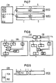
- FIG. 3 shows a control system CTSYS, which has four control devices SD0 ... SD3 with the channel-side data paths of the associated channels CH1 ... CH8 of the channel system which run in both transmission directions CHSYS according to FIG 1.
- the control information that specifies the various possible data paths is stored in a communication memory that can be controlled by all control devices SD0 ... SD3 via a communication bus CBS.
- SD3 can, for example, form the bit masks for the individual release of the ports A, B, C, D of two control devices, for example IPC0 and IPC1, which are coupled to one another by a further communication bus CBI, from the stored information Disk storage of an input / output system are connected.
- control devices IPC0, IPC1 run parallel to all four control devices SD0 ... SD3, there can be several options for reconnection for each disk memory of an input / output system.
- the control devices of other input / output systems, e.g. IPCn and IPCn-1 are connected to the control devices SD0 ... SD3 by serial daisy chains of their associated ports.
- Which of the two control devices, e.g. IPC0 and IPC1, which each receive the interrupt signal (RPS) from the addressed disk memory, intends to carry out the data transfer, is decided on the basis of the bit masks stored in the common control memory for the individual ports and depending on the current occupancy of the control devices.
- the selected control device, e.g. IPC0 delivers the interrupt signal for the connected control devices to the permitted port addresses, e.g. SD0 and SD1.
- FIG. 4 shows a control system CTSYS, in which the device-related control devices IPC0 ... IPCn are connected directly to the channels of the channel system.
- the channel itself carries out the conversion of the path group commands into bit masks for the ports A ... D of the individual control devices.
- the device- and operation-specific parameters and the command-dependent control information from which the masks are derived are stored, for example, in a separate memory area (subchannel) of the main memory, which is reserved for administration entries for the individual memory devices.
- the selection of the data paths on the device side and the determination of the one data path on the channel side for establishing the return connection is carried out in the same way as in the control systems CTSYS according to FIG. 2 and FIG. 3.
- the control system CTSYS in FIG 5 consists only of channel-side control devices SD0 ... SD3, which is connected to an intermediate control unit CU for controlling the disk memories PS0 ... PSn of an input / output system IOS.
- Any disk storage e.g. In contrast to the disk memories according to FIG. 1, PS0 has four device connection paths, via which the interrupt signal (RPS) is sent in parallel to the control unit CU and from there to the connected control devices SD0 ... SD3.
- RPS interrupt signal
- the determination of the one channel-side data path with the associated channel is in turn carried out on the basis of the control information specified by the path group commands, which in the all control devices SD0 ... SD3 common communication memory are stored.
- the control unit CU is only used to convert the control parameters associated with the triggered input / output operation into control signals for the individual disk memories PS0 ... PSn.
- the storage of selection information and of data to be taken over from the controlled disk storage or to be transferred to it in the device-related control devices of the control systems according to FIGS. 2, 3 and 4 does not take place.
- the data to be transferred from or transferred to the disk memory can be temporarily stored in the control devices SD0 ... SD3.
- the system shown in FIG. 5 can also be implemented for disk memories with only two device connection paths, so that in this case two control devices, e.g., for receiving the interrupt signal (RPS) SD0 and SD1 are sufficient.
- RPS interrupt signal
- driver circuits TSA, TSB are arranged at the interface to, for example, the channel-side control devices and a driver circuit TSD for supplying one of the two device connection paths of a disk memory.
- the data to be transferred from or transferred to the disk storage are stored in one data store BUF each.
- the communication interface between the two control devices IPC0, IPC1 is formed by the common control memory CTM which can be controlled via the communication bus CBI and which contains, among other things, the selection information in the form of bit masks for the individual release of the ports.
- This control memory CTM can be read and written by each central control unit IDC arranged in a control device.
- the central control unit IDC has a processor that controls the entire data flow in the control device and controls from and to the connected units.
- the selection information DSI1 ... DSI8 is entered.
- a maximum of eight devices can be connected in an input / output system.
- an area in the control memory CTM of a predetermined size is reserved in which this device-specific information, e.g. DSI1.
- the control memory CTM contains further information, which is defined in each case for an input / output operation and a storage device.
- the information LCKIN for each device can cause the associated device-specific information to remain blocked for access.
- the RESIN and ASSIN information also stored in the control memory CTM, it is possible to explicitly and implicitly reserve a specific device for data transmission, so that the device cannot be dynamically allocated to perform input / output operations.
- the information DSI1 ... DSI8 allow the selection of individual ports in the device-related control devices for the data transfer from and to the storage devices.
- the selection information DSI1 ... DSI8 are formed by bit masks which individually define the release of the associated ports A, B or A ... D for each of the storage devices D1 ... D8 connected to the two control devices, and thus the selection of the device-side Enable data paths for the reconnection.
- the entry in the memory CTM consists of two bytes BYIPC0, BYIPC1 for each of the two control devices.
- Each mask has four bit positions, which are each composed of the corresponding bit positions D1 ... D8 for the four ports, for example A ... D.
- the structure of the channel-side control devices essentially corresponds to that of the control devices near the device. 8, driver circuits TS are likewise arranged in each of the control devices SD0, SD1 at the interfaces to the channels and to the control devices.
- a control unit ICC controls the data flow and access to the memories BUF and COM.
- the communication memory COM which can be controlled jointly by all control devices, is only arranged in control systems CTSYS according to FIG. 3 or FIG. 5.
- the information which can be read by all control devices in the communication memory COM contains a memory block DCB in which control information PGIN and PGID are entered for each connected disk memory.
- the control information PGID has identification characters for each of the possible channel-side data paths, which are each grouped into path groups for establishing the return connection.
- the existing control information PGIN each includes information about the mode PM of a path group, which indicates whether the establishment of a return connection is only possible via one path or about different paths of a group of paths, and information PGC, which characterize the formation and resolution of a path group.
Landscapes
- Engineering & Computer Science (AREA)
- Theoretical Computer Science (AREA)
- Physics & Mathematics (AREA)
- General Engineering & Computer Science (AREA)
- General Physics & Mathematics (AREA)
- Human Computer Interaction (AREA)
- Signal Processing For Digital Recording And Reproducing (AREA)
- Multi Processors (AREA)
- Facsimiles In General (AREA)
- Bus Control (AREA)
- Exchange Systems With Centralized Control (AREA)
Claims (10)
- Procédé d'exécution d'opérations d'entrée/sortie dans des systèmes de traitement de données, dans lequel respectivement une opération d'entrée/sortie est dirigée par une unité de traitement d'entrée/sortie (IOP) vers un système d'entrée/sortie périphérique existant (IOS), comprenant des appareils de mémoire rotatifs, en particulier des mémoires à disques (PS0...PSn) et poursuivie par une transmission de données vers un appareil de mémoire sélectionné ou à partir de ce dernier, dès qu'une liaison de retour entre l'un des appareils de mémoire reliés à un système de commande (CTSYS) et à un système à canaux (CHSYS) couplé à l'unité de traitement d'entrée/sortie (IOP) et comprenant plusieurs canaux (par exemple CH1...CH8) est établie (reconnexion dynamique) par des voies de données parallèles, prévues dans le système de commande, respectivement dans le système à canaux (CTSYS, respectivement CHSYS), du côté des appareils, respectivement du côté des canaux, caractérisé en ce que- quelques voies sont déterminées à l'aide d'informations de commande et de sélection (PGIN, PGID et Dsl1.....DSI8) à partir des voies de données respectivement parallèles, pour l'établissement de la liaison de retour du système de commande (CTSYS), étant précisé que, parmi les voies de données du côté des canaux, seule une voie est sélectionnée dans chaque cas pour la reconnexion par le canal afférent du système à canaux (CHSYS) et occupée d'une exigence d'établissement de la liaison de retour, et- en ce que des moyens (BUF) de mise en mémoire intermédiaire des données à reprendre par l'appareil de mémoire ou à transmettre à l'appareil de mémoire sont mis à la disposition dans le système de commande (CTSYS).
- Procédé selon la revendication 1, caractérisé en ce que les informations de commande (PGIN, PGID) caractérisent les voies de données, du côté des canaux, qui peuvent, dans chaque cas, être sélectionnées pour l'établissement de la liaison de retour.
- Procédé selon la revendication 2, caractérisé en ce que les informations de commande (PGIN, PGID) sont déduites d'instructions par lesquelles des groupes de voies avec diverses voies de données possibles, du côté des canaux, sont prédéterminés dans chaque cas pour l'établissement de la liaison de retour.
- Procédé selon la revendication 1, caractérisé en ce que les informations de sélection (DSI1....DSI8) indiquent dans le système de commande (CTSYS) les voies de données du côté des appareils, pouvant être sélectionnées dans chaque cas pour l'établissement de la liaison de retour.
- Procédé selon les revendications 3 et 4, caractérisé en ce que les informations de sélection (DSI1.....DSI8) sont déduites d'instructions pour la détermination des groupes de voies.
- Procédé selon l'une des revendications 2 à 5, caractérisé en ce que, dans un système de commande (CTSYS) avec des dispositifs de contrôle (par exemple IPC0, IPC1), à proximité des appareils, pour la commande du système d'entrée/sortie (IOS), les informations de sélection (DsI1....DSI8) sont constituées de masques binaires (BYIPC0, BYIPC1) qui déterminent individuellement, pour chaque appareil de mémoire raccordé, la sélection des différentes voies de données, du côté des appareils, dans le système de commande, et sont inscrites dans une mémoire de commande (CTM) commune aux dispositifs de commande.
- Procédé selon la revendication 6, caractérisé en ce que les moyens (BUF) de mise en mémoire intermédiaire des données sont disponibles dans chaque dispositif de contrôle (par exemple IPC0....IPCn) lors d'une transmission des données à partir de l'appareil de mémoire ou vers cet appareil.
- Procédé selon la revendication 6 ou 7, caractérisé en ce que, si les dispositifs de contrôle à proximité des appareils (par exemple IPC0, IPC1) sont directement couplés au système à canaux (CHSYS) par les voies de données du côté des canaux, les informations de commande (PGIN, PGID) sont déposées dans un dispositif de mémoire prévu pour la réception d'entrées de gestion pour les différents appareils de mémoire.
- Procédé selon l'une des revendications 2 à 7, caractérisé en ce que, dans un système de commande (CTSYS) avec dispositifs de commande du côté des canaux (par exemple SD0...SD3) pour la commande des voies de données du côté des canaux à partir des canaux afférents (par exemple CH1....CH8) du système à canaux (CHSYS) et vers ces canaux, les informations de commande (PGIN, PGID) sont mises en mémoire dans une mémoire de communication (COM) commune à tous les dispositifs de commande et en ce que la sélection de la voie de données du côté des canaux, prévue pour l'établissement de la liaison de retour, se fait par détermination d'un dispositif de commande libre (par exemple SD0), à l'aide des informations de commande mises en mémoire.
- Procédé selon l'une des revendications 2 à 5, caractérisé en ce que, dans un système de commande (CTSYS) comprenant uniquement des dispositifs de commande (par exemple SD0....SD3) du côté des canaux, pour la commande des voies de données du côté des canaux, à partir des canaux afférents et vers ces canaux (par exemple CH1....CH8) du système à canaux (CHSYS), les informations de commande (PGIN, PGID) sont mises en mémoire dans une mémoire de communication (COM) commune à tous les dispositifs de commande, et en ce que, à l'aide des informations de commande mises en mémoire, la sélection de la voie de données du côté des canaux, prévue pour l'établissement de la liaison de retour, se fait par détermination d'un dispositif de commande libre (par exemple SD0) et en ce que les moyens (BUF) pour la mise en mémoire intermédiaire des données d'une transmission des données à partir de l'appareil de mémoire ou vers cet appareil, sont disponibles dans tous les dispositifs de commande (par exemple SD0...SD3).
Priority Applications (4)
| Application Number | Priority Date | Filing Date | Title |
|---|---|---|---|
| DE59108554T DE59108554D1 (de) | 1991-08-13 | 1991-08-13 | Verfahren zur Durchführung von Ein-/Ausgabeoperationen in Datenverarbeitungssystemen |
| EP91113605A EP0528060B1 (fr) | 1991-08-13 | 1991-08-13 | Procédé d'exécution d'operations d'entrée/sortie dans des systèmes de traitement de données |
| ES91113605T ES2097775T3 (es) | 1991-08-13 | 1991-08-13 | Procedimiento para la realizacion de operaciones de entrada/salida en sistemas de proceso de datos. |
| AT91113605T ATE149062T1 (de) | 1991-08-13 | 1991-08-13 | Verfahren zur durchführung von ein- /ausgabeoperationen in datenverarbeitungssystemen |
Applications Claiming Priority (1)
| Application Number | Priority Date | Filing Date | Title |
|---|---|---|---|
| EP91113605A EP0528060B1 (fr) | 1991-08-13 | 1991-08-13 | Procédé d'exécution d'operations d'entrée/sortie dans des systèmes de traitement de données |
Publications (2)
| Publication Number | Publication Date |
|---|---|
| EP0528060A1 EP0528060A1 (fr) | 1993-02-24 |
| EP0528060B1 true EP0528060B1 (fr) | 1997-02-19 |
Family
ID=8207042
Family Applications (1)
| Application Number | Title | Priority Date | Filing Date |
|---|---|---|---|
| EP91113605A Expired - Lifetime EP0528060B1 (fr) | 1991-08-13 | 1991-08-13 | Procédé d'exécution d'operations d'entrée/sortie dans des systèmes de traitement de données |
Country Status (4)
| Country | Link |
|---|---|
| EP (1) | EP0528060B1 (fr) |
| AT (1) | ATE149062T1 (fr) |
| DE (1) | DE59108554D1 (fr) |
| ES (1) | ES2097775T3 (fr) |
Families Citing this family (2)
| Publication number | Priority date | Publication date | Assignee | Title |
|---|---|---|---|---|
| JP3224326B2 (ja) * | 1994-06-24 | 2001-10-29 | 富士通株式会社 | ディスク装置及びディスクサブシステム |
| WO1997007464A1 (fr) * | 1995-08-11 | 1997-02-27 | Siemens Nixdorf Informationssysteme Ag | Agencement pour le raccordement de memoires peripheriques |
Family Cites Families (1)
| Publication number | Priority date | Publication date | Assignee | Title |
|---|---|---|---|---|
| US4400773A (en) * | 1980-12-31 | 1983-08-23 | International Business Machines Corp. | Independent handling of I/O interrupt requests and associated status information transfers |
-
1991
- 1991-08-13 ES ES91113605T patent/ES2097775T3/es not_active Expired - Lifetime
- 1991-08-13 EP EP91113605A patent/EP0528060B1/fr not_active Expired - Lifetime
- 1991-08-13 AT AT91113605T patent/ATE149062T1/de not_active IP Right Cessation
- 1991-08-13 DE DE59108554T patent/DE59108554D1/de not_active Expired - Fee Related
Also Published As
| Publication number | Publication date |
|---|---|
| EP0528060A1 (fr) | 1993-02-24 |
| ES2097775T3 (es) | 1997-04-16 |
| ATE149062T1 (de) | 1997-03-15 |
| DE59108554D1 (de) | 1997-03-27 |
Similar Documents
| Publication | Publication Date | Title |
|---|---|---|
| DE3300261C2 (fr) | ||
| DE3642324C2 (de) | Multiprozessoranlage mit Prozessor-Zugriffssteuerung | |
| DE3300260C2 (fr) | ||
| EP1101329B1 (fr) | Module de pontage | |
| DE4003759C2 (de) | Verfahren und Anordnung zur Übertragung von Daten über einen Bus zwischen selektiv ankoppelbaren Stationen | |
| DE2523372B2 (de) | Eingabe-ZAusgabe-Anschlußsteuereinrichtung | |
| DE3241376A1 (de) | Dma-steuereinrichtung zur uebertragung von daten zwischen einem datensender und einem datenempfaenger | |
| EP0315919B1 (fr) | Noeud de commutation pour la commutation de signaux de données contenus dans des paquets de données | |
| EP0329005A1 (fr) | Procédé pour l'établissement de circuits virtuels à travers les commutateurs d'un dispositif de commutation à plusieurs étages | |
| DE69119149T2 (de) | Struktur zur direkten Speicher-zu-Speicher-Übertragung | |
| EP0062141B1 (fr) | Circuit pour l'entrée de signaux de commande d'exécution dans un système de micro-ordinateur | |
| EP0185260B1 (fr) | Interface pour le transfert direct d'informations | |
| DE3936339C2 (de) | DMA-Controller | |
| DE69524320T2 (de) | Digitale Kommunikationsein- und ausgangsschnittstelle | |
| DE3142504A1 (de) | Mehrfachplattenspeicher-uebertragungssystem | |
| EP0291789A1 (fr) | Montage de circuit pour centraux de télécommunication multiplex à division dans le temps, en particulier des centraux téléphoniques MIC avec des groupes de connexion connectés à un réseau de commutation | |
| EP0409330B1 (fr) | Circuit de commande d'accès d'une mémoire | |
| EP0528060B1 (fr) | Procédé d'exécution d'operations d'entrée/sortie dans des systèmes de traitement de données | |
| DE2845218B1 (de) | Mikroprogrammgesteuerte Ein-/Ausgabeeinrichtung und Verfahren zum Durchfuehren von Ein-/Ausgabeoperationen | |
| DE4122831C2 (de) | Integrierte Halbleiterschaltung | |
| EP0048869A2 (fr) | Système de multiprocesseur, en particulier comprenant un nombre de microprocesseurs | |
| EP0045043B1 (fr) | Commande de la connexion d'un canal | |
| DE10027845B4 (de) | Submodul für die Kontrolle einer Datenwarteschlange | |
| EP1334432A1 (fr) | Systeme de communication pour echanger des donnees au moyen d'un processeur supplementaire | |
| DE3935707A1 (de) | System zur verbindung von rechnern mit ihrer peripheren ausruestung |
Legal Events
| Date | Code | Title | Description |
|---|---|---|---|
| PUAI | Public reference made under article 153(3) epc to a published international application that has entered the european phase |
Free format text: ORIGINAL CODE: 0009012 |
|
| AK | Designated contracting states |
Kind code of ref document: A1 Designated state(s): AT BE CH DE DK ES FR GB GR IT LI LU NL SE |
|
| RBV | Designated contracting states (corrected) |
Designated state(s): AT BE CH DE ES FR GB IT LI NL SE |
|
| 17P | Request for examination filed |
Effective date: 19930324 |
|
| 17Q | First examination report despatched |
Effective date: 19951123 |
|
| GRAG | Despatch of communication of intention to grant |
Free format text: ORIGINAL CODE: EPIDOS AGRA |
|
| GRAH | Despatch of communication of intention to grant a patent |
Free format text: ORIGINAL CODE: EPIDOS IGRA |
|
| GRAH | Despatch of communication of intention to grant a patent |
Free format text: ORIGINAL CODE: EPIDOS IGRA |
|
| GRAA | (expected) grant |
Free format text: ORIGINAL CODE: 0009210 |
|
| AK | Designated contracting states |
Kind code of ref document: B1 Designated state(s): AT BE CH DE ES FR GB IT LI NL SE |
|
| REF | Corresponds to: |
Ref document number: 149062 Country of ref document: AT Date of ref document: 19970315 Kind code of ref document: T |
|
| REG | Reference to a national code |
Ref country code: CH Ref legal event code: NV Representative=s name: SIEMENS SCHWEIZ AG Ref country code: CH Ref legal event code: EP |
|
| REF | Corresponds to: |
Ref document number: 59108554 Country of ref document: DE Date of ref document: 19970327 |
|
| REG | Reference to a national code |
Ref country code: ES Ref legal event code: FG2A Ref document number: 2097775 Country of ref document: ES Kind code of ref document: T3 |
|
| ET | Fr: translation filed | ||
| ITF | It: translation for a ep patent filed | ||
| GBT | Gb: translation of ep patent filed (gb section 77(6)(a)/1977) |
Effective date: 19970423 |
|
| PG25 | Lapsed in a contracting state [announced via postgrant information from national office to epo] |
Ref country code: SE Effective date: 19970519 |
|
| PGFP | Annual fee paid to national office [announced via postgrant information from national office to epo] |
Ref country code: GB Payment date: 19970715 Year of fee payment: 7 |
|
| PGFP | Annual fee paid to national office [announced via postgrant information from national office to epo] |
Ref country code: AT Payment date: 19970723 Year of fee payment: 7 |
|
| PGFP | Annual fee paid to national office [announced via postgrant information from national office to epo] |
Ref country code: ES Payment date: 19970808 Year of fee payment: 7 |
|
| PGFP | Annual fee paid to national office [announced via postgrant information from national office to epo] |
Ref country code: NL Payment date: 19970821 Year of fee payment: 7 |
|
| PGFP | Annual fee paid to national office [announced via postgrant information from national office to epo] |
Ref country code: BE Payment date: 19970822 Year of fee payment: 7 |
|
| PGFP | Annual fee paid to national office [announced via postgrant information from national office to epo] |
Ref country code: FR Payment date: 19970827 Year of fee payment: 7 |
|
| PGFP | Annual fee paid to national office [announced via postgrant information from national office to epo] |
Ref country code: CH Payment date: 19971119 Year of fee payment: 7 |
|
| PLBE | No opposition filed within time limit |
Free format text: ORIGINAL CODE: 0009261 |
|
| STAA | Information on the status of an ep patent application or granted ep patent |
Free format text: STATUS: NO OPPOSITION FILED WITHIN TIME LIMIT |
|
| 26N | No opposition filed | ||
| PG25 | Lapsed in a contracting state [announced via postgrant information from national office to epo] |
Ref country code: GB Free format text: LAPSE BECAUSE OF NON-PAYMENT OF DUE FEES Effective date: 19980813 Ref country code: AT Free format text: LAPSE BECAUSE OF NON-PAYMENT OF DUE FEES Effective date: 19980813 |
|
| PG25 | Lapsed in a contracting state [announced via postgrant information from national office to epo] |
Ref country code: ES Free format text: LAPSE BECAUSE OF NON-PAYMENT OF DUE FEES Effective date: 19980814 |
|
| PG25 | Lapsed in a contracting state [announced via postgrant information from national office to epo] |
Ref country code: LI Free format text: LAPSE BECAUSE OF NON-PAYMENT OF DUE FEES Effective date: 19980831 Ref country code: CH Free format text: LAPSE BECAUSE OF NON-PAYMENT OF DUE FEES Effective date: 19980831 Ref country code: BE Free format text: LAPSE BECAUSE OF NON-PAYMENT OF DUE FEES Effective date: 19980831 |
|
| BERE | Be: lapsed |
Owner name: SIEMENS NIXDORF INFORMATIONSSYSTEME A.G. Effective date: 19980831 |
|
| PG25 | Lapsed in a contracting state [announced via postgrant information from national office to epo] |
Ref country code: NL Free format text: LAPSE BECAUSE OF NON-PAYMENT OF DUE FEES Effective date: 19990301 |
|
| GBPC | Gb: european patent ceased through non-payment of renewal fee |
Effective date: 19980813 |
|
| REG | Reference to a national code |
Ref country code: CH Ref legal event code: PL |
|
| PG25 | Lapsed in a contracting state [announced via postgrant information from national office to epo] |
Ref country code: FR Free format text: LAPSE BECAUSE OF NON-PAYMENT OF DUE FEES Effective date: 19990430 |
|
| NLV4 | Nl: lapsed or anulled due to non-payment of the annual fee |
Effective date: 19990301 |
|
| REG | Reference to a national code |
Ref country code: FR Ref legal event code: ST |
|
| PGFP | Annual fee paid to national office [announced via postgrant information from national office to epo] |
Ref country code: DE Payment date: 20010719 Year of fee payment: 11 |
|
| PG25 | Lapsed in a contracting state [announced via postgrant information from national office to epo] |
Ref country code: DE Free format text: LAPSE BECAUSE OF NON-PAYMENT OF DUE FEES Effective date: 20030301 |
|
| REG | Reference to a national code |
Ref country code: ES Ref legal event code: FD2A Effective date: 19990910 |
|
| PG25 | Lapsed in a contracting state [announced via postgrant information from national office to epo] |
Ref country code: IT Free format text: LAPSE BECAUSE OF NON-PAYMENT OF DUE FEES Effective date: 20050813 |