EP0528596A1 - Procédé pour fabriquer des dispositifs à effet de champ comportant des grilles ultra-courtes et dispositif ainsi fabriqué - Google Patents
Procédé pour fabriquer des dispositifs à effet de champ comportant des grilles ultra-courtes et dispositif ainsi fabriqué Download PDFInfo
- Publication number
- EP0528596A1 EP0528596A1 EP92307201A EP92307201A EP0528596A1 EP 0528596 A1 EP0528596 A1 EP 0528596A1 EP 92307201 A EP92307201 A EP 92307201A EP 92307201 A EP92307201 A EP 92307201A EP 0528596 A1 EP0528596 A1 EP 0528596A1
- Authority
- EP
- European Patent Office
- Prior art keywords
- layer
- gate
- quantum well
- field effect
- substrate
- Prior art date
- Legal status (The legal status is an assumption and is not a legal conclusion. Google has not performed a legal analysis and makes no representation as to the accuracy of the status listed.)
- Withdrawn
Links
Images

Classifications
-
- H—ELECTRICITY
- H10—SEMICONDUCTOR DEVICES; ELECTRIC SOLID-STATE DEVICES NOT OTHERWISE PROVIDED FOR
- H10D—INORGANIC ELECTRIC SEMICONDUCTOR DEVICES
- H10D30/00—Field-effect transistors [FET]
- H10D30/01—Manufacture or treatment
- H10D30/021—Manufacture or treatment of FETs having insulated gates [IGFET]
-
- H—ELECTRICITY
- H10—SEMICONDUCTOR DEVICES; ELECTRIC SOLID-STATE DEVICES NOT OTHERWISE PROVIDED FOR
- H10D—INORGANIC ELECTRIC SEMICONDUCTOR DEVICES
- H10D30/00—Field-effect transistors [FET]
- H10D30/01—Manufacture or treatment
- H10D30/015—Manufacture or treatment of FETs having heterojunction interface channels or heterojunction gate electrodes, e.g. HEMT
-
- H—ELECTRICITY
- H10—SEMICONDUCTOR DEVICES; ELECTRIC SOLID-STATE DEVICES NOT OTHERWISE PROVIDED FOR
- H10D—INORGANIC ELECTRIC SEMICONDUCTOR DEVICES
- H10D30/00—Field-effect transistors [FET]
- H10D30/40—FETs having zero-dimensional [0D], one-dimensional [1D] or two-dimensional [2D] charge carrier gas channels
- H10D30/47—FETs having zero-dimensional [0D], one-dimensional [1D] or two-dimensional [2D] charge carrier gas channels having two-dimensional [2D] charge carrier gas channels, e.g. nanoribbon FETs or high electron mobility transistors [HEMT]
- H10D30/471—High electron mobility transistors [HEMT] or high hole mobility transistors [HHMT]
- H10D30/473—High electron mobility transistors [HEMT] or high hole mobility transistors [HHMT] having confinement of carriers by multiple heterojunctions, e.g. quantum well HEMT
- H10D30/4732—High electron mobility transistors [HEMT] or high hole mobility transistors [HHMT] having confinement of carriers by multiple heterojunctions, e.g. quantum well HEMT using Group III-V semiconductor material
-
- H—ELECTRICITY
- H10—SEMICONDUCTOR DEVICES; ELECTRIC SOLID-STATE DEVICES NOT OTHERWISE PROVIDED FOR
- H10D—INORGANIC ELECTRIC SEMICONDUCTOR DEVICES
- H10D30/00—Field-effect transistors [FET]
- H10D30/80—FETs having rectifying junction gate electrodes
- H10D30/87—FETs having Schottky gate electrodes, e.g. metal-semiconductor FETs [MESFET]
- H10D30/871—Vertical FETs having Schottky gate electrodes
-
- H—ELECTRICITY
- H10—SEMICONDUCTOR DEVICES; ELECTRIC SOLID-STATE DEVICES NOT OTHERWISE PROVIDED FOR
- H10D—INORGANIC ELECTRIC SEMICONDUCTOR DEVICES
- H10D62/00—Semiconductor bodies, or regions thereof, of devices having potential barriers
- H10D62/60—Impurity distributions or concentrations
- H10D62/605—Planar doped, e.g. atomic-plane doped or delta-doped
-
- H—ELECTRICITY
- H10—SEMICONDUCTOR DEVICES; ELECTRIC SOLID-STATE DEVICES NOT OTHERWISE PROVIDED FOR
- H10D—INORGANIC ELECTRIC SEMICONDUCTOR DEVICES
- H10D62/00—Semiconductor bodies, or regions thereof, of devices having potential barriers
- H10D62/80—Semiconductor bodies, or regions thereof, of devices having potential barriers characterised by the materials
- H10D62/85—Semiconductor bodies, or regions thereof, of devices having potential barriers characterised by the materials being Group III-V materials, e.g. GaAs
-
- Y—GENERAL TAGGING OF NEW TECHNOLOGICAL DEVELOPMENTS; GENERAL TAGGING OF CROSS-SECTIONAL TECHNOLOGIES SPANNING OVER SEVERAL SECTIONS OF THE IPC; TECHNICAL SUBJECTS COVERED BY FORMER USPC CROSS-REFERENCE ART COLLECTIONS [XRACs] AND DIGESTS
- Y10—TECHNICAL SUBJECTS COVERED BY FORMER USPC
- Y10S—TECHNICAL SUBJECTS COVERED BY FORMER USPC CROSS-REFERENCE ART COLLECTIONS [XRACs] AND DIGESTS
- Y10S148/00—Metal treatment
- Y10S148/053—Field effect transistors fets
Definitions
- This invention relates to a method for making field effect devices with ultrashort gates and to devices made thereby.
- Field effect devices such as field effect transistors
- field effect transistors are fundamental components in modern electronics. They are basic components in most digital and many analog circuits, including circuits for data processing and telecommunications. Indeed it has been surmised that field effect transistors are among the most numerous of man-made objects.
- Field effect devices typically comprise a conductive path between a source and a drain.
- a region of the path between the source and the drain, called the channel is under the control of the electric field produced by a gate electrode.
- the source and the drain can be n-type regions in the surface of a semiconductor substrate and the channel can be a shallow n-type region connecting them.
- a gate electrode formed on a thin insulator overlying the channel can be used to control the electrical properties of the channel. If no voltage is applied to the gate, current can flow from the source through the channel to the drain. However if a sufficient negative voltage is applied to the gate, electrons will be forced from the channel region, thereby depleting it of carriers and reducing or even shutting off the source-drain current.
- the highest operating frequency of such a device and, concomitantly its speed as a switch is determined in large part by the shortness of the gate-channel region.
- a method for making field effect devices such as a field effect transistors, having ultrashort gate lengths so low as five hundred angstroms or less.
- the gate structure is grown on a substrate by thin film deposition so that the length dimension of the gate is perpendicular to a major surface of the substrate.
- An edge of the gate-containing substrate is exposed, and the structure comprising the source, drain and channel is grown on the edge.
- field effect devices with precisely controlled gate lengths of less than 100 angstroms are achievable.
- the active regions of the device can be immersed within semiconductor material so that surface properties do not deteriorate device performance.
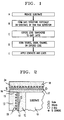
- FIG. 1 illustrates the steps in making a field effect device
- FIG. 2 is a schematic cross section of an exemplary field effect device made in accordance with the process of FIG. 1.
- the first step is to provide a substrate (10 of FIG. 2) which is preferably an undoped monocrystalline semiconductor, such as gallium arsenide, having a pair of major surfaces.
- a substrate (10 of FIG. 2) which is preferably an undoped monocrystalline semiconductor, such as gallium arsenide, having a pair of major surfaces.
- the second step, shown in FIG. 1B, is to deposit the gate structure on the substrate by thin film deposition so that the length dimension of the gate is perpendicular to a major surface of the substrate 10.
- the gate structure is a thin conductive layer 12 disposed between a pair of spacer layers 11 and 13 of non-conductive material.
- layer 12 is a two dimensional electron gas layer comprised of a quantum well. Electrons for the well can be provided by delta doping of the adjacent spacer layers 11, 13. Alternatively, dopants can be introduced directly into the quantum well.
- the structure can be conveniently deposited using molecular beam epitaxy (MBE) to grow on the substrate 10 an inner spacer layer 11 such as aluminum gallium arsenide, a conductive gate layer 12 such as a gallium arsenide quantum well region and an outer spacer layer 13 such as aluminum gallium arsenide.
- MBE molecular beam epitaxy
- One or both of the spacer layers 11, 13 can include delta doping 23 with donors, such as silicon, to provide electrons to well 12.
- the gate layer 12 is advantageously less than about 500 angstroms thick.
- the next step is to expose an edge 15 of the resulting structure transverse to the first conductive layer 12.
- the substrate is preferably cleaved to provide a pristine edge surface 15.
- the workpiece can be etched to expose an edge transverse to layer 12.
- the fourth step, shown in FIG. 1D, is to deposit on the exposed edge 15 of the gate-containing substrate, the source, drain and channel structure comprising a third spacer layer 16 of non-conductive material, a second thin conductive layer 17 and an outer spacer layer 18 of non-conductive material.
- Spacer layer 16 can be deposited by growing aluminum gallium arsenide on the exposed edge surface transverse to gate layer 12.
- Conductive source-drain-channel layer 17 is preferably a second two dimensional electron gas layer comprising a quantum well region, such as gallium arsenide, grown on layer 16, and outer spacer layer 18 can be aluminum gallium arsenide grown over conductive layer 17.
- One or both of the spacer regions 16, 18 can include delta doping 24 with donors to provide electrons to well 17.
- Spacer 16 is advantageously less than about 250 angstroms thick.
- the final step is to provide electrical contacts to gate layer 12 and to source-drain layer 17 on opposite sides of the gate, thereby defining the gate, source and drain, respectively, of a field effect device.
- FIG. 3 is a perspective view of the metallized device of FIG. 1 showing the gate contact 20, the source contact 21, and the drain contact 22.
- contacts are made with the quantum well electron gas regions 12 and 17 by depositing AuGeNi ohmic contacts, and an outer layer of subsequently deposited gold can lead away from the contacts.
- the contacts and leads are deposited and configured by techniques well known in the art.
- the resulting structure acts as a depletion mode field-effect transistor.
- the width of the gate is controlled not by lithography but rather by the thickness of the deposited layers 12 and 17.
- thin film deposition techniques such as molecular beam epitaxy permit the fabrication of atomically smooth layers of atomically precise thickness.
- atomically precise gate lengths of less than 500 angstroms and even less than 100 angstroms can be achieved by this method.
- the conductive layers are remotely doped and are free of mobility-reducing dopant ions, the carriers have a high mobility, leading to low resistance of the gate and the source-drain channel.
- the active region of the field effect device -- the region constituting the gate controlled channel -- is completely immersed within non-conductive material, e.g. the aluminum gallium arsenide spacer layers. Surface properties and Schottky barriers do not deteriorate device performance.
- An embedded gate structure is formed by providing a (100) gallium arsenide substrate and growing on the substrate by molecular beam epitaxy (MBE), the following sequence of layers: 4.3 micrometers of undoped Al 0.3 Ga 0.7 As, 200 angstroms of undoped GaAs, 150 angstroms of Al 0.3 Ga 0.7 As, a delta doped silicon layer of a concentration 1.5 x 1012 cm ⁇ 2, and 20 micrometers of undoped Al 0.3 Ga 0.7 As.
- the 200 angstrom layer of GaAs is a quantum well containing a two-dimensional electron gas. It is buried 20 micrometers below the surface and acts as a gate.
- the electron gas quantum well region has a carrier density at 77K of about 4. 3 x 1011 cm ⁇ 2 and a mobility of about 1.3 x 105 cm2 /V sec.
- the gallium arsenide substrate can be thinned, as by lapping from the backside, to a thickness of about 150 micrometers, and cleaved into a rectangular piece approximately 5mm by 10mm.
- the substrate is preferably cleaved in situ within an MBE growth chamber to expose a pristine (110) surface transverse and substantially perpendicular to the plane of the 200 angstrom electron gas quantum well region.
- the procedural details and apparatus required for this in situ cleaving process are described in Pfeiffer et al, "Formation of a High Quality Two-Dimensional Electron Gas on Cleaved GaAs," 56 Applied Physics Letters 17 (April 20, 1990).
- the source, drain channel structure is then grown on the freshly cleaved edge by MBE deposition of a 200 angstrom layer of an undoped Al 0.44 Ga 0.56 As spacer, a 150 angstrom undoped GaAs quantum well, a 150 angstrom undoped Al 0.3 Ga 0.7 As spacer layer, followed by a Si delta-doped layer of concentration 2x 1012cm ⁇ 2, 1700 angstroms of undoped Al 0.3 Ga 0.7 As and 600 angstroms of undoped GaAs.
- This process generates a 150 angstrom wide modulation-doped quantum well source-drain channel separated from the gate 12 by a 200 angstrom AlGaAs layer.
- the estimated electron density for the electron gas quantum well at 77K is 1.5x 1011 cm ⁇ 2 with mobility 3.9x 104cm2/V sec.
- FIG. 4 shows the transistor characteristics of the device at 77K.
- the transistor exhibits a transconductance of 196mS/mm.
Landscapes
- Junction Field-Effect Transistors (AREA)
Applications Claiming Priority (2)
| Application Number | Priority Date | Filing Date | Title |
|---|---|---|---|
| US07/745,589 US5219772A (en) | 1991-08-15 | 1991-08-15 | Method for making field effect devices with ultra-short gates |
| US745589 | 1991-08-15 |
Publications (1)
| Publication Number | Publication Date |
|---|---|
| EP0528596A1 true EP0528596A1 (fr) | 1993-02-24 |
Family
ID=24997348
Family Applications (1)
| Application Number | Title | Priority Date | Filing Date |
|---|---|---|---|
| EP92307201A Withdrawn EP0528596A1 (fr) | 1991-08-15 | 1992-08-06 | Procédé pour fabriquer des dispositifs à effet de champ comportant des grilles ultra-courtes et dispositif ainsi fabriqué |
Country Status (3)
| Country | Link |
|---|---|
| US (2) | US5219772A (fr) |
| EP (1) | EP0528596A1 (fr) |
| JP (1) | JP2558418B2 (fr) |
Families Citing this family (6)
| Publication number | Priority date | Publication date | Assignee | Title |
|---|---|---|---|---|
| US5308997A (en) * | 1992-06-22 | 1994-05-03 | Motorola, Inc. | Self-aligned thin film transistor |
| US5323020A (en) * | 1992-12-22 | 1994-06-21 | International Business Machines Corporation | High performance MESFET with multiple quantum wells |
| US7781801B2 (en) * | 2006-09-25 | 2010-08-24 | Alcatel-Lucent Usa Inc. | Field-effect transistors whose gate electrodes are over semiconductor heterostructures and parts of source and drain electrodes |
| CN102104002B (zh) * | 2009-12-16 | 2013-04-24 | 中国科学院微电子研究所 | 一种制备极短栅长体硅围栅MOSFETs的方法 |
| US9041060B2 (en) | 2013-07-25 | 2015-05-26 | International Business Machines Corporation | III-V FET device with overlapped extension regions using gate last |
| US9246112B2 (en) * | 2014-01-08 | 2016-01-26 | International Business Machines Corporation | Semiconductor device with ballistic gate length structure |
Citations (3)
| Publication number | Priority date | Publication date | Assignee | Title |
|---|---|---|---|---|
| EP0051504A1 (fr) * | 1980-10-31 | 1982-05-12 | Thomson-Csf | Transistors à effet de champ à grille ultra courte |
| GB2110876A (en) * | 1981-12-07 | 1983-06-22 | Western Electric Co | Formation of submicron features in semiconductor devices |
| EP0179196A2 (fr) * | 1984-06-22 | 1986-04-30 | International Business Machines Corporation | Procédé de fabrication d'un dispositif semi-conducteur utilisant un masque |
Family Cites Families (8)
| Publication number | Priority date | Publication date | Assignee | Title |
|---|---|---|---|---|
| JPS605570A (ja) * | 1983-06-09 | 1985-01-12 | Fujitsu Ltd | 半導体装置の製造方法 |
| US4791072A (en) * | 1984-06-15 | 1988-12-13 | American Telephone And Telegraph Company, At&T Bell Laboratories | Method for making a complementary device containing MODFET |
| US4882609A (en) * | 1984-11-19 | 1989-11-21 | Max-Planck Gesellschaft Zur Forderung Der Wissenschafter E.V. | Semiconductor devices with at least one monoatomic layer of doping atoms |
| US4631560A (en) * | 1984-12-19 | 1986-12-23 | Eaton Corporation | MOMS tunnel emission transistor |
| US4701996A (en) * | 1984-12-19 | 1987-10-27 | Calviello Joseph A | Method for fabricating edge channel FET |
| EP0214047B1 (fr) * | 1985-08-20 | 1993-12-22 | Fujitsu Limited | Transistor à effet de champ |
| US4821093A (en) * | 1986-08-18 | 1989-04-11 | The United States Of America As Represented By The Secretary Of The Army | Dual channel high electron mobility field effect transistor |
| US5130766A (en) * | 1988-08-04 | 1992-07-14 | Fujitsu Limited | Quantum interference type semiconductor device |
-
1991
- 1991-08-15 US US07/745,589 patent/US5219772A/en not_active Expired - Lifetime
-
1992
- 1992-08-06 EP EP92307201A patent/EP0528596A1/fr not_active Withdrawn
- 1992-08-12 JP JP4235183A patent/JP2558418B2/ja not_active Expired - Fee Related
- 1992-12-29 US US07/997,816 patent/US5311045A/en not_active Expired - Lifetime
Patent Citations (3)
| Publication number | Priority date | Publication date | Assignee | Title |
|---|---|---|---|---|
| EP0051504A1 (fr) * | 1980-10-31 | 1982-05-12 | Thomson-Csf | Transistors à effet de champ à grille ultra courte |
| GB2110876A (en) * | 1981-12-07 | 1983-06-22 | Western Electric Co | Formation of submicron features in semiconductor devices |
| EP0179196A2 (fr) * | 1984-06-22 | 1986-04-30 | International Business Machines Corporation | Procédé de fabrication d'un dispositif semi-conducteur utilisant un masque |
Non-Patent Citations (3)
| Title |
|---|
| APPLIED PHYSICS LETTERS. vol. 58, no. 7, 18 February 1991, NEW YORK US pages 726 - 728 H.L. STORMER ET AL. 'Atomically precise superlattice potential imposed on a two-dimensional electron gas.' * |
| HARTSTEIN A., ET AL.: "A METAL-OXIDE-SEMICONDUCTOR FIELD-EFFECT TRANSISTOR WITH A 20-NM CHANNEL LENGTH.", JOURNAL OF APPLIED PHYSICS, AMERICAN INSTITUTE OF PHYSICS, US, vol. 68., no. 05., 1 September 1990 (1990-09-01), US, pages 2493 - 2495., XP000108779, ISSN: 0021-8979, DOI: 10.1063/1.346512 * |
| JOURNAL OF CRYSTAL GROWTH. vol. 111, 1991, AMSTERDAM NL pages 333 - 338 L. PFEIFFER ET AL. 'Quantum wire structures by MBE overgrowth on a cleaved edge.' * |
Also Published As
| Publication number | Publication date |
|---|---|
| US5311045A (en) | 1994-05-10 |
| JPH07142508A (ja) | 1995-06-02 |
| US5219772A (en) | 1993-06-15 |
| JP2558418B2 (ja) | 1996-11-27 |
Similar Documents
| Publication | Publication Date | Title |
|---|---|---|
| US4711858A (en) | Method of fabricating a self-aligned metal-semiconductor FET having an insulator spacer | |
| JP2599381B2 (ja) | Fetデバイスの製造方法 | |
| US7244973B2 (en) | Field-effect semiconductor device and method for making the same | |
| US5036017A (en) | Method of making asymmetrical field effect transistor | |
| EP0143656A2 (fr) | Dispositif semi-conducteur à semi-conducteurs composés et procédé de fabrication | |
| US4389768A (en) | Self-aligned process for fabricating gallium arsenide metal-semiconductor field effect transistors | |
| JP2504376B2 (ja) | 電界効果型トランジスタ | |
| JP3376078B2 (ja) | 高電子移動度トランジスタ | |
| EP0201873B1 (fr) | Procédé de fabrication d'un transistor à effet de champ métal-semi-conducteur et transistor ainsi obtenu | |
| US3866310A (en) | Method for making the self-aligned gate contact of a semiconductor device | |
| US5336626A (en) | Method of manufacturing a MESFET with an epitaxial void | |
| US5219772A (en) | Method for making field effect devices with ultra-short gates | |
| US8288260B1 (en) | Field effect transistor with dual etch-stop layers for improved power, performance and reproducibility | |
| EP0602671A2 (fr) | Transistor à effet de champ à hétérojonction ayant des caractéristiques de transistor améliorées | |
| JP2701583B2 (ja) | トンネルトランジスタ及びその製造方法 | |
| JP2822400B2 (ja) | 半導体装置 | |
| GB2239557A (en) | High electron mobility transistors | |
| JPH0212927A (ja) | Mes fetの製造方法 | |
| JPH04233771A (ja) | 電界効果トランジスタ及びその製造方法 | |
| KR950001167B1 (ko) | 화합물 반도체소자 및 그 제조방법 | |
| JP2658513B2 (ja) | 電界効果トランジスタ | |
| JP3077653B2 (ja) | 電界効果トランジスタ及びその製造方法 | |
| JP2001524759A (ja) | ガリウムひ素ベースのエピタキシャル電界効果トランジスタの選択性凹部用InxGa1−xPエッチング停止層及びその製造方法 | |
| KR950001168B1 (ko) | 화합물 반도체 장치 및 그 제조방법 | |
| KR950001165B1 (ko) | 화합물 반도체소자 및 그 제조방법 |
Legal Events
| Date | Code | Title | Description |
|---|---|---|---|
| PUAI | Public reference made under article 153(3) epc to a published international application that has entered the european phase |
Free format text: ORIGINAL CODE: 0009012 |
|
| AK | Designated contracting states |
Kind code of ref document: A1 Designated state(s): DE FR GB |
|
| 17P | Request for examination filed |
Effective date: 19930811 |
|
| RAP3 | Party data changed (applicant data changed or rights of an application transferred) |
Owner name: AT&T CORP. |
|
| 17Q | First examination report despatched |
Effective date: 19950531 |
|
| GRAG | Despatch of communication of intention to grant |
Free format text: ORIGINAL CODE: EPIDOS AGRA |
|
| GRAG | Despatch of communication of intention to grant |
Free format text: ORIGINAL CODE: EPIDOS AGRA |
|
| GRAH | Despatch of communication of intention to grant a patent |
Free format text: ORIGINAL CODE: EPIDOS IGRA |
|
| GRAH | Despatch of communication of intention to grant a patent |
Free format text: ORIGINAL CODE: EPIDOS IGRA |
|
| STAA | Information on the status of an ep patent application or granted ep patent |
Free format text: STATUS: THE APPLICATION IS DEEMED TO BE WITHDRAWN |
|
| 18D | Application deemed to be withdrawn |
Effective date: 20010301 |