EP0528651A2 - Circuit de pompe de charge adaptatif pour boucles à verrouillage de phase - Google Patents
Circuit de pompe de charge adaptatif pour boucles à verrouillage de phase Download PDFInfo
- Publication number
- EP0528651A2 EP0528651A2 EP92307433A EP92307433A EP0528651A2 EP 0528651 A2 EP0528651 A2 EP 0528651A2 EP 92307433 A EP92307433 A EP 92307433A EP 92307433 A EP92307433 A EP 92307433A EP 0528651 A2 EP0528651 A2 EP 0528651A2
- Authority
- EP
- European Patent Office
- Prior art keywords
- phase
- current
- charge pump
- magnitude
- locked loop
- Prior art date
- Legal status (The legal status is an assumption and is not a legal conclusion. Google has not performed a legal analysis and makes no representation as to the accuracy of the status listed.)
- Withdrawn
Links
Images

Classifications
-
- H—ELECTRICITY
- H03—ELECTRONIC CIRCUITRY
- H03L—AUTOMATIC CONTROL, STARTING, SYNCHRONISATION OR STABILISATION OF GENERATORS OF ELECTRONIC OSCILLATIONS OR PULSES
- H03L7/00—Automatic control of frequency or phase; Synchronisation
- H03L7/06—Automatic control of frequency or phase; Synchronisation using a reference signal applied to a frequency- or phase-locked loop
- H03L7/08—Details of the phase-locked loop
- H03L7/085—Details of the phase-locked loop concerning mainly the frequency- or phase-detection arrangement including the filtering or amplification of its output signal
- H03L7/095—Details of the phase-locked loop concerning mainly the frequency- or phase-detection arrangement including the filtering or amplification of its output signal using a lock detector
-
- H—ELECTRICITY
- H03—ELECTRONIC CIRCUITRY
- H03L—AUTOMATIC CONTROL, STARTING, SYNCHRONISATION OR STABILISATION OF GENERATORS OF ELECTRONIC OSCILLATIONS OR PULSES
- H03L7/00—Automatic control of frequency or phase; Synchronisation
- H03L7/06—Automatic control of frequency or phase; Synchronisation using a reference signal applied to a frequency- or phase-locked loop
- H03L7/08—Details of the phase-locked loop
- H03L7/10—Details of the phase-locked loop for assuring initial synchronisation or for broadening the capture range
- H03L7/107—Details of the phase-locked loop for assuring initial synchronisation or for broadening the capture range using a variable transfer function for the loop, e.g. low pass filter having a variable bandwidth
- H03L7/1072—Details of the phase-locked loop for assuring initial synchronisation or for broadening the capture range using a variable transfer function for the loop, e.g. low pass filter having a variable bandwidth by changing characteristics of the charge pump, e.g. changing the gain
-
- H—ELECTRICITY
- H03—ELECTRONIC CIRCUITRY
- H03L—AUTOMATIC CONTROL, STARTING, SYNCHRONISATION OR STABILISATION OF GENERATORS OF ELECTRONIC OSCILLATIONS OR PULSES
- H03L7/00—Automatic control of frequency or phase; Synchronisation
- H03L7/06—Automatic control of frequency or phase; Synchronisation using a reference signal applied to a frequency- or phase-locked loop
- H03L7/08—Details of the phase-locked loop
- H03L7/085—Details of the phase-locked loop concerning mainly the frequency- or phase-detection arrangement including the filtering or amplification of its output signal
- H03L7/089—Details of the phase-locked loop concerning mainly the frequency- or phase-detection arrangement including the filtering or amplification of its output signal the phase or frequency detector generating up-down pulses
- H03L7/0891—Details of the phase-locked loop concerning mainly the frequency- or phase-detection arrangement including the filtering or amplification of its output signal the phase or frequency detector generating up-down pulses the up-down pulses controlling source and sink current generators, e.g. a charge pump
- H03L7/0895—Details of the current generators
- H03L7/0898—Details of the current generators the source or sink current values being variable
-
- H—ELECTRICITY
- H03—ELECTRONIC CIRCUITRY
- H03L—AUTOMATIC CONTROL, STARTING, SYNCHRONISATION OR STABILISATION OF GENERATORS OF ELECTRONIC OSCILLATIONS OR PULSES
- H03L7/00—Automatic control of frequency or phase; Synchronisation
- H03L7/06—Automatic control of frequency or phase; Synchronisation using a reference signal applied to a frequency- or phase-locked loop
- H03L7/16—Indirect frequency synthesis, i.e. generating a desired one of a number of predetermined frequencies using a frequency- or phase-locked loop
- H03L7/18—Indirect frequency synthesis, i.e. generating a desired one of a number of predetermined frequencies using a frequency- or phase-locked loop using a frequency divider or counter in the loop
- H03L7/183—Indirect frequency synthesis, i.e. generating a desired one of a number of predetermined frequencies using a frequency- or phase-locked loop using a frequency divider or counter in the loop a time difference being used for locking the loop, the counter counting between fixed numbers or the frequency divider dividing by a fixed number
Definitions
- the present invention relates generally to phase-locked loops and more specifically to charge pumps for phase-locked loops.
- a basic phase-locked loop is a circuit which produces an output signal synchronized to an input reference signal.
- a PLL output signal is synchronized or "locked" to a reference signal when the frequency of the output signal is the same as that of the reference signal.
- a PLL may provide for a constant phase difference between the reference and output signals. This phase difference may assume any desired value including zero. Should a deviation in the desired phase difference of such signals develop ( i.e. , should a phase error develop) due to, e.g. , variation in either (i) the frequency of the reference signal or (ii) programmable parameters of the PLL, the PLL will attempt to adjust the frequency of its output signal to drive the phase error toward zero.
- PLLs There are several different types of PLLs. Among these are PLLs which are charge pump-based.
- a phase-frequency detector compares an input reference signal to an output signal from a voltage controlled oscillator for the purpose of observing phase and frequency differences between the signals. If differences are observed, the phase-frequency detector produces logic pulses indicative of such differences.
- a charge pump receives these logic pulses and, based thereon, provides pulses of current to a loop filter and ultimately the voltage controlled oscillator. As filtered, these current pulses serve to adjust the voltage controlled oscillator to compensate for the observed differences.
- the magnitude of PLL bandwidth is a parameter detecting PLL performance.
- the present invention provides a method and apparatus for temporarily providing an increased PLL bandwidth responsive to variations or transients in a reference signal or programmable loop parameters, and a narrow bandwidth during the steady-state.
- An illustrative embodiment of the present invention comprises an adaptive charge pump which operates to employ a relationship between the magnitude of charge pump current and PLL bandwidth. This relationship provides that increases in charge pump current tend to increase PLL bandwidth, while decreases in current tend to decrease PLL bandwidth.
- the embodiment provides for sensing the above-described variations and, responsive thereto, temporarily increasing the magnitude of charge pump current.
- the increased charge pump current increases PLL bandwidth and therefore decreases settling time of a PLL in response to such variations.
- the charge pump current is reduced, reducing PLL bandwidth and steady- state phase jitter.
- the temporary nature of an increase in charge pump current provides for enhanced PLL settling properties, as needed, without a sustained increase in PLL steady-state phase jitter.
- the illustrative embodiment of the present invention functions by operation of a variation sensor in combination with a variable current source.
- the variation sensor monitors the outputs of a PLL's phase-frequency detector for the presence of logic pulses indicating a variation to be tracked. Responsive to sensing significant logic pulses, the variation sensor signals the variable current source that increased current should be provided to the loop filter and VCO of the PLL to improve settling time.
- the viable current source responds by increasing the magnitude of its output current pulses, thereby increasing PLL bandwidth and providing for quicker adjustment to the sensed variation.
- the voltage controlled oscillator of the PLL responds to the filtered current pulses by adjusting its output to track the variation, significant logic pulses from the phase-frequency detector cease.
- the variation sensor responds to the lack of significant logic pulses by de-asserting its signal to the variable current source, which, in response, reduces the magnitude of current pulses it produces.
- the present invention has use in many systems such as clock signal synthesizer systems for, among other things, video graphics applications.
- Figure 1 presents an illustrative charge pump-based phase- locked loop.
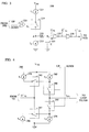
- Figure 2 presents an illustrative embodiment of the adaptive charge pump of the present invention.
- Figure 3 presents an illustrative variation sensor.
- Figure 4 presents an illustrative variable current source.
- FIG. 1 An illustrative charge pump-based phase-locked loop (PLL) 50 is presented in Figure 1.
- a reference signal U I is received by a digital programmable divider circuit 75, which divides the frequency of U I by a programmable value N.
- a resulting signal, U IN is provided to a phase-frequency detector (PFD) 100.
- PFD 10 Also provided to the PFD 10 is signal U OM , which is the output of a voltage controlled oscillator (VCO) 400, U O , divided by a number M by another digital programmable divider circuit 500.
- PFD 100 detects differences in phase and frequency between U IN and U OM , and provides logic signals to an embodiment of an adaptive charge pump 200 indicating when such differences have been detected. By arbitrary convention these logic signals are designated as DOWN and UP, respectively. (It will be apparent to one of ordinary skill in the art that the opposite convention could be chosen.)
- the adaptive charge pump 200 is coupled to a loop filter 300 and provides a charge pump output current, I CO , to the loop filter 300 based on the received UP/DOWN logic signals.
- the loop filter 300 provides low-pass filtering to I CO , yielding a filtered signal U F . This signal is provided as feed-back to the VCO 400.
- the digital programmable dividers 75 and 500 in the illustrative embodiment may be any of those well known in the art.
- the illustrative PFD 100 may be any of the well-known types, such as that presented in Figure 6.18 in F.M. Gardener, Phaselock Techniques , 123-25 (1979).
- the loop filter 300 of the illustrative embodiment is a first order low-pass filter.
- the illustrative VCO 400 comprises a voltage to current converter coupled to a ring oscillator which comprises three current controlled inverters.
- UP/DOWN logic signals from PFD 100 are provided to both a variation sensor (VS) 220 and a variable current source (VCS) 260.
- the VS 220 is coupled to VCS 260, and both are coupled to a power supply voltage, V DD .
- the VS 220 sends a variation signal, U′ VS , to the VCS 260.
- the VCS 260 provides output current I CO to the loop filter 300 of the PLL 50.
- FIG. 3 An illustrative VS 220 is presented in Figure 3. As shown in the Figure, the UP/DOWN logic signals from the PFD 100 are logically ORed by gate 225 to form signal S1. Signal S1 controls the operation of a switch 229, which in turn modulates the flow of current, I1, from current source 227. Switch 229 will close during the intervals when signal S1 is logically true. Resistor 235 is coupled to switch 229 at node A, along with current source 233. Capacitor 231 is coupled to resistor 235 at node B.
- the voltage signal at node B is designated as U VS .
- This signal is received by inverter 237 which provides as output a logical TRUE signal whenever it receives an input signal which is less than or equal to a threshold, V th .
- Inverter 237 will provide as output a logical FALSE signal whenever it receives an input signal which is greater than V th . Because of this threshold, the inverted signal output from inverter 237 is indicated with a "prime” notation: U ⁇ ′ VS .
- This output is again inverted by inverter 239 to provide signal U′ VS . It is this signal, U′ VS , which is output to the VCS 260.
- VCS 260 includes two current sources, 265 and 275, which are directly modulated by the UP and DOWN logic pulse signals from the PFD 100 by operation of switches 290 and 292, respectively.
- VCS 260 also includes two current sources 270 and 280 which are modulated not only by the UP and DOWN logic pulse signals applied to switches 290 and 292, respectively, but also by signal U′ VS , by operation of switches 285 and 287, respectively.
- Exemplary values for I3 and I4 are 4 ⁇ A and 20 ⁇ A, respectively.
- the output current of the VCS 260 may comprise current from either of sources 265 or 275, depending on the presence or absence of UP or DOWN logic pulse signals controlling switches 290 or 292, respectively.
- the output current of the VCS 260 may comprise current from either of sources 265 or 275, depending on the presence or absence of UP or DOWN logic pulse signals, plus current from either source 270 or 280.
- current sources controlled by switches in the VCS 260 and the VS 220 may comprise separate switches and sources, as presented in Figures 3 and 4, or unified switched current sources. Whether separate or together as a single element, such may be formed with field effect transistors using techniques well known in the art.
- the PFD 100 will cease generating significant UP/DOWN logic pulses. Absent such significant logic pulses, the voltage at node B of the VCS 260, U VS , is driven toward zero by current source 233. The condition of U VS ⁇ V th is sensed by the threshold logic of inverter 237 causing it to provide a logical TRUE signal as output. This signal is inverted by inverter 239 to a logical FALSE signal causing switches 285 and 287 to open.
- VCS 260 may provide output current equal to I3 from sources 265 and 275, depending on the presence of UP/DOWN logic pulses at switches 290 and 292, respectively. Responsive to this level of output current, the PLL 50 exhibits a reduced level of phase jitter compared with that exhibited by the PLL 50 when its output current equals the sum of I3 and I4.
Landscapes
- Stabilization Of Oscillater, Synchronisation, Frequency Synthesizers (AREA)
Applications Claiming Priority (2)
| Application Number | Priority Date | Filing Date | Title |
|---|---|---|---|
| US07/748,136 US5208546A (en) | 1991-08-21 | 1991-08-21 | Adaptive charge pump for phase-locked loops |
| US748136 | 2000-12-27 |
Publications (2)
| Publication Number | Publication Date |
|---|---|
| EP0528651A2 true EP0528651A2 (fr) | 1993-02-24 |
| EP0528651A3 EP0528651A3 (en) | 1993-09-15 |
Family
ID=25008180
Family Applications (1)
| Application Number | Title | Priority Date | Filing Date |
|---|---|---|---|
| EP19920307433 Withdrawn EP0528651A3 (en) | 1991-08-21 | 1992-08-13 | Adaptive charge pump for phase-locked loops |
Country Status (3)
| Country | Link |
|---|---|
| US (1) | US5208546A (fr) |
| EP (1) | EP0528651A3 (fr) |
| TW (1) | TW205610B (fr) |
Cited By (7)
| Publication number | Priority date | Publication date | Assignee | Title |
|---|---|---|---|---|
| EP0647033A1 (fr) * | 1993-10-04 | 1995-04-05 | Nec Corporation | Circuit de synchronisation de phase présentant un temps d'accrochage réduit et une faible gigue |
| EP0788236A1 (fr) * | 1996-01-30 | 1997-08-06 | Nec Corporation | Synthétiseur de fréquence à PLL avec contrÔle de gain du circuit de pompe de charge |
| WO2000002317A1 (fr) * | 1998-07-01 | 2000-01-13 | Conexant Systems, Inc. | Procede et appareil de reglage de decalage de phase dans une boucle a phase asservie |
| EP1143623A1 (fr) * | 2000-04-07 | 2001-10-10 | Nec Corporation | Procédé et dispositif de comparaison de phase adaptatif pour boucles à verrouillage de phase |
| EP1292032A4 (fr) * | 2000-06-05 | 2003-08-20 | Mitsubishi Electric Corp | Dispositif synchrone |
| WO2004075414A1 (fr) * | 2003-02-14 | 2004-09-02 | Mcdonald James J Iii | Ensemble de circuits pour reduction du temps d'acquisition d'une pll |
| DE102004031913A1 (de) * | 2004-06-21 | 2006-01-05 | Atmel Germany Gmbh | Ladungspumpe einer Phasenregelschleife mit umschaltbarer Systembandbreite und Verfahren zur Steuerung einer solchen Ladungspumpe |
Families Citing this family (49)
| Publication number | Priority date | Publication date | Assignee | Title |
|---|---|---|---|---|
| JP2993200B2 (ja) * | 1991-07-31 | 1999-12-20 | 日本電気株式会社 | 位相同期ループ |
| JP2854777B2 (ja) * | 1992-04-27 | 1999-02-03 | 株式会社東芝 | 位相同期ループ回路と信号抽出方法 |
| DE4216714A1 (de) * | 1992-05-20 | 1993-12-02 | Siemens Ag | Verfahren zum Einstellen von PLL-Parametern |
| US5384550A (en) * | 1992-09-18 | 1995-01-24 | Rockwell International Corporation | Loop transient response estimator for improved acquisition performance |
| US5414745A (en) * | 1993-06-01 | 1995-05-09 | Advanced Micro Devices, Inc. | Synchronized clocking disable and enable circuit |
| US6288602B1 (en) * | 1993-06-25 | 2001-09-11 | International Business Machines Corporation | CMOS on-chip precision voltage reference scheme |
| US5448598A (en) * | 1993-07-06 | 1995-09-05 | Standard Microsystems Corporation | Analog PLL clock recovery circuit and a LAN transceiver employing the same |
| JP2682401B2 (ja) * | 1993-10-28 | 1997-11-26 | 日本電気株式会社 | クロック信号発生回路 |
| DE4342344C2 (de) * | 1993-12-11 | 1996-07-25 | Telefunken Microelectron | Schaltungsanordnung für eine Phasenregelschleife |
| US5703539A (en) * | 1993-12-17 | 1997-12-30 | Motorola, Inc. | Apparatus and method for controlling the loop bandwidth of a phase locked loop |
| TW379293B (en) * | 1994-04-01 | 2000-01-11 | Ibm | Apparatus and method for generating a clock in a microprocessor |
| US5646563A (en) * | 1994-07-15 | 1997-07-08 | National Semiconductor Corporation | Charge pump with near zero offset current |
| US5495207A (en) * | 1994-08-31 | 1996-02-27 | International Business Machines Corporation | Differential current controlled oscillator with variable load |
| US5491439A (en) * | 1994-08-31 | 1996-02-13 | International Business Machines Corporation | Method and apparatus for reducing jitter in a phase locked loop circuit |
| US5619161A (en) * | 1994-08-31 | 1997-04-08 | International Business Machines Corporation | Diffrential charge pump with integrated common mode control |
| US5513225A (en) * | 1994-08-31 | 1996-04-30 | International Business Machines Corporation | Resistorless phase locked loop circuit employing direct current injection |
| US5525932A (en) * | 1994-08-31 | 1996-06-11 | International Business Machines Corporation | Lock indicator for phase locked loop circuit |
| US5815016A (en) * | 1994-09-02 | 1998-09-29 | Xilinx, Inc. | Phase-locked delay loop for clock correction |
| US5646564A (en) * | 1994-09-02 | 1997-07-08 | Xilinx, Inc. | Phase-locked delay loop for clock correction |
| US5479458A (en) * | 1994-10-05 | 1995-12-26 | Tanaka; Yoshiaki | Digital phase shifter including 1/N for phase detect and subsequent VCO adjust |
| US5805002A (en) * | 1995-01-24 | 1998-09-08 | Ic Works, Inc. | Slow transition time phase frequency detector and method |
| DE19515218A1 (de) * | 1995-04-28 | 1996-10-31 | Thomson Brandt Gmbh | Verfahren zur Abstimmung einer Oszillatoreinrichtung für wenigstens zwei Abstimmfrequenzen sowie Schaltungsanordnung zur Durchführung des Verfahrens |
| US5694062A (en) * | 1996-02-02 | 1997-12-02 | Lsi Logic Corporation | Self-timed phase detector and method |
| JP2877196B2 (ja) * | 1996-03-28 | 1999-03-31 | 日本電気株式会社 | チャージポンプ回路およびそれを備えた位相同期回路 |
| JP3395818B2 (ja) * | 1996-04-19 | 2003-04-14 | ソニー株式会社 | Pll回路とそれを用いた信号処理装置 |
| JP3481051B2 (ja) * | 1996-06-19 | 2003-12-22 | 富士通株式会社 | チャージポンプ回路、および、該チャージポンプ回路を有するpll回路並びに半導体集積回路 |
| US5663689A (en) * | 1996-06-26 | 1997-09-02 | International Business Machines Corporation | Method and apparatus for providing a high speed charge pump with low static error |
| TW363305B (en) * | 1996-09-06 | 1999-07-01 | Koninkl Philips Electronics Nv | A receiver, a frequency synthesis circuit and a charge pump |
| KR100224577B1 (ko) * | 1996-10-07 | 1999-10-15 | 윤종용 | 위상동기루프의 록 검출장치 |
| US5831484A (en) * | 1997-03-18 | 1998-11-03 | International Business Machines Corporation | Differential charge pump for phase locked loop circuits |
| US6002273A (en) * | 1998-10-05 | 1999-12-14 | Motorola, Inc. | Linear low noise phase-frequency detector |
| US6327319B1 (en) | 1998-11-06 | 2001-12-04 | Motorola, Inc. | Phase detector with frequency steering |
| DE19935905A1 (de) * | 1999-07-30 | 2001-02-08 | Motorola Inc | Elektrisches Filter mit Kondensator und Steuereinheit sowie Verfahren zum Betreiben des Filters |
| JP4771572B2 (ja) * | 2000-04-10 | 2011-09-14 | 富士通セミコンダクター株式会社 | Pll半導体装置並びにその試験の方法及び装置 |
| US6456165B1 (en) | 2000-08-18 | 2002-09-24 | International Business Machines Corporation | Phase error control for phase-locked loops |
| ATE422729T1 (de) * | 2000-12-28 | 2009-02-15 | Renesas Tech Corp | Pll-schaltung mit reduzierter einschwingzeit |
| US7062004B1 (en) * | 2001-06-06 | 2006-06-13 | Silicon Image, Inc. | Method and apparatus for adaptive control of PLL loop bandwidth |
| US6657917B2 (en) * | 2001-07-02 | 2003-12-02 | Micron Technology, Inc. | Selective adjustment of voltage controlled oscillator gain in a phase-locked loop |
| US6614318B1 (en) * | 2001-11-05 | 2003-09-02 | Xilinx, Inc. | Voltage controlled oscillator with jitter correction |
| DE10303939B3 (de) * | 2003-01-31 | 2004-05-13 | Infineon Technologies Ag | Schaltungsanordnung mit Phasendetektor und Phasenregelschleife mit der Schaltungsanordnung |
| US6806742B1 (en) * | 2003-05-23 | 2004-10-19 | Standard Microsystems Corporation | Phase detector for low power applications |
| CN1741389B (zh) * | 2004-08-26 | 2014-06-11 | 瑞昱半导体股份有限公司 | 具有非线性相位误差反应特性的锁相环 |
| JP2008078995A (ja) * | 2006-09-21 | 2008-04-03 | Nec Electronics Corp | 移相回路 |
| US7570105B1 (en) * | 2007-10-04 | 2009-08-04 | Altera Corporation | Variable current charge pump with modular switch circuit |
| GB0804342D0 (en) * | 2008-03-07 | 2008-04-16 | Cambridge Silicon Radio Ltd | Charge transfer in a phase-locked loop |
| TWI415394B (zh) * | 2010-04-13 | 2013-11-11 | Elite Semiconductor Esmt | 鎖相迴路電路及其操作方法 |
| TWI427933B (zh) * | 2011-03-18 | 2014-02-21 | Realtek Semiconductor Corp | 鎖相迴路及其方法 |
| EP3243277B1 (fr) * | 2015-01-05 | 2022-07-20 | Telefonaktiebolaget LM Ericsson (publ) | Procédé et noeud de réseau radio pour compensation pour traction ou poussée d'oscillateur local |
| US9419632B1 (en) * | 2016-04-22 | 2016-08-16 | Via Alliance Semiconductor Co., Ltd. | Charge pump for use in phase-locked loop |
Family Cites Families (10)
| Publication number | Priority date | Publication date | Assignee | Title |
|---|---|---|---|---|
| US3610954A (en) * | 1970-11-12 | 1971-10-05 | Motorola Inc | Phase comparator using logic gates |
| US4122405A (en) * | 1977-10-21 | 1978-10-24 | National Semiconductor Corporation | Digital logic level signal indication of phase and frequency lock condition in a phase-locked loop |
| US4156855A (en) * | 1978-01-26 | 1979-05-29 | Rca Corporation | Phase-locked loop with variable gain and bandwidth |
| JPS5827438A (ja) * | 1981-08-12 | 1983-02-18 | Fujitsu Ltd | Pll回路 |
| US4745372A (en) * | 1985-10-17 | 1988-05-17 | Matsushita Electric Industrial Co., Ltd. | Phase-locked-loop circuit having a charge pump |
| US4890072A (en) * | 1988-02-03 | 1989-12-26 | Motorola, Inc. | Phase locked loop having a fast lock current reduction and clamping circuit |
| US4885554A (en) * | 1988-12-16 | 1989-12-05 | Tektronix, Inc. | Phase-offset signal generator |
| US4920320A (en) * | 1988-12-19 | 1990-04-24 | Motorola, Inc. | Phase locked loop with optimally controlled bandwidth |
| US4926141A (en) * | 1989-05-01 | 1990-05-15 | Motorola, Inc. | Frequency synthesizer with improved automatic control of loop bandwidth selection |
| DE69129946T2 (de) * | 1990-05-21 | 1999-04-15 | Nec Corp., Tokio/Tokyo | Phasenregelkreisschaltung |
-
1991
- 1991-08-21 US US07/748,136 patent/US5208546A/en not_active Expired - Lifetime
- 1991-10-21 TW TW080108290A patent/TW205610B/zh active
-
1992
- 1992-08-13 EP EP19920307433 patent/EP0528651A3/en not_active Withdrawn
Cited By (10)
| Publication number | Priority date | Publication date | Assignee | Title |
|---|---|---|---|---|
| EP0647033A1 (fr) * | 1993-10-04 | 1995-04-05 | Nec Corporation | Circuit de synchronisation de phase présentant un temps d'accrochage réduit et une faible gigue |
| EP0788236A1 (fr) * | 1996-01-30 | 1997-08-06 | Nec Corporation | Synthétiseur de fréquence à PLL avec contrÔle de gain du circuit de pompe de charge |
| US5831483A (en) * | 1996-01-30 | 1998-11-03 | Nec Corporation | PLL frequency synthesizer having circuit for controlling gain of charge pump circuit |
| WO2000002317A1 (fr) * | 1998-07-01 | 2000-01-13 | Conexant Systems, Inc. | Procede et appareil de reglage de decalage de phase dans une boucle a phase asservie |
| EP1143623A1 (fr) * | 2000-04-07 | 2001-10-10 | Nec Corporation | Procédé et dispositif de comparaison de phase adaptatif pour boucles à verrouillage de phase |
| EP1292032A4 (fr) * | 2000-06-05 | 2003-08-20 | Mitsubishi Electric Corp | Dispositif synchrone |
| US6812754B1 (en) | 2000-06-05 | 2004-11-02 | Renesas Technology Corp. | Clock synchronizer with offset prevention function against variation of output potential of loop filter |
| WO2004075414A1 (fr) * | 2003-02-14 | 2004-09-02 | Mcdonald James J Iii | Ensemble de circuits pour reduction du temps d'acquisition d'une pll |
| US6940356B2 (en) | 2003-02-14 | 2005-09-06 | Fairchild Semiconductor Corporation | Circuitry to reduce PLL lock acquisition time |
| DE102004031913A1 (de) * | 2004-06-21 | 2006-01-05 | Atmel Germany Gmbh | Ladungspumpe einer Phasenregelschleife mit umschaltbarer Systembandbreite und Verfahren zur Steuerung einer solchen Ladungspumpe |
Also Published As
| Publication number | Publication date |
|---|---|
| TW205610B (fr) | 1993-05-11 |
| EP0528651A3 (en) | 1993-09-15 |
| US5208546A (en) | 1993-05-04 |
Similar Documents
| Publication | Publication Date | Title |
|---|---|---|
| US5208546A (en) | Adaptive charge pump for phase-locked loops | |
| EP0482823B1 (fr) | Synthétiseur de fréquence à PLL permettant de changer la fréquence de sortie à une vitesse élevée | |
| US5648744A (en) | System and method for voltage controlled oscillator automatic band selection | |
| US4590602A (en) | Wide range clock recovery circuit | |
| US5831483A (en) | PLL frequency synthesizer having circuit for controlling gain of charge pump circuit | |
| US5381116A (en) | Method and apparatus for performing frequency tracking in an all digital phase lock loop | |
| US5955928A (en) | Automatically adjusting the dynamic range of the VCO in a PLL at start-up for optimal operating point | |
| US6667663B2 (en) | Phase locked loop circuit | |
| US5838205A (en) | Variable-speed phase-locked loop system with on-the-fly switching and method therefor | |
| US6226339B1 (en) | Method and system for detecting phase lock in a phase-locked loop | |
| US6774732B1 (en) | System and method for coarse tuning a phase locked loop (PLL) synthesizer using 2-PI slip detection | |
| JPH07303042A (ja) | Pll周波数シンセサイザ | |
| JP3331115B2 (ja) | 周波数位相同期回路 | |
| US5436596A (en) | PLL with stable phase discriminator | |
| US6456165B1 (en) | Phase error control for phase-locked loops | |
| US6373912B1 (en) | Phase-locked loop arrangement with fast lock mode | |
| US20020008586A1 (en) | PLL Frequency synthesizer circuit | |
| JP4342754B2 (ja) | Pll回路 | |
| US20040151271A1 (en) | Phase-locked loop control circuit | |
| US20020163395A1 (en) | Phase-locked loop frequency synthesizer | |
| US20030214330A1 (en) | Phase-locked loop circuit | |
| US6285260B1 (en) | Phase-locked loop having circuit for synchronizing starting points of two counters | |
| EP0599372B1 (fr) | PLL comportant un discriminateur de phase stable | |
| US20070241825A1 (en) | Phase Locked Loop Circuit | |
| KR100498411B1 (ko) | 주파수동기제어방법및이를수행하는위상동기루프 |
Legal Events
| Date | Code | Title | Description |
|---|---|---|---|
| PUAI | Public reference made under article 153(3) epc to a published international application that has entered the european phase |
Free format text: ORIGINAL CODE: 0009012 |
|
| AK | Designated contracting states |
Kind code of ref document: A2 Designated state(s): DE ES FR GB IT NL |
|
| PUAL | Search report despatched |
Free format text: ORIGINAL CODE: 0009013 |
|
| AK | Designated contracting states |
Kind code of ref document: A3 Designated state(s): DE ES FR GB IT NL |
|
| 17P | Request for examination filed |
Effective date: 19940303 |
|
| RAP3 | Party data changed (applicant data changed or rights of an application transferred) |
Owner name: AT&T CORP. |
|
| 17Q | First examination report despatched |
Effective date: 19950705 |
|
| STAA | Information on the status of an ep patent application or granted ep patent |
Free format text: STATUS: THE APPLICATION HAS BEEN WITHDRAWN |
|
| 18W | Application withdrawn |
Withdrawal date: 19951013 |