EP0529602A2 - Récepteur différentiel, tolérant les défauts de lignes - Google Patents
Récepteur différentiel, tolérant les défauts de lignes Download PDFInfo
- Publication number
- EP0529602A2 EP0529602A2 EP92114529A EP92114529A EP0529602A2 EP 0529602 A2 EP0529602 A2 EP 0529602A2 EP 92114529 A EP92114529 A EP 92114529A EP 92114529 A EP92114529 A EP 92114529A EP 0529602 A2 EP0529602 A2 EP 0529602A2
- Authority
- EP
- European Patent Office
- Prior art keywords
- output
- transmission lines
- multiplex transmission
- transmission apparatus
- multiplex
- Prior art date
- Legal status (The legal status is an assumption and is not a legal conclusion. Google has not performed a legal analysis and makes no representation as to the accuracy of the status listed.)
- Granted
Links
Images


Classifications
-
- H—ELECTRICITY
- H04—ELECTRIC COMMUNICATION TECHNIQUE
- H04L—TRANSMISSION OF DIGITAL INFORMATION, e.g. TELEGRAPHIC COMMUNICATION
- H04L25/00—Baseband systems
- H04L25/02—Details ; arrangements for supplying electrical power along data transmission lines
- H04L25/08—Modifications for reducing interference; Modifications for reducing effects due to line faults ; Receiver end arrangements for detecting or overcoming line faults
-
- B—PERFORMING OPERATIONS; TRANSPORTING
- B60—VEHICLES IN GENERAL
- B60R—VEHICLES, VEHICLE FITTINGS, OR VEHICLE PARTS, NOT OTHERWISE PROVIDED FOR
- B60R16/00—Electric or fluid circuits specially adapted for vehicles and not otherwise provided for; Arrangement of elements of electric or fluid circuits specially adapted for vehicles and not otherwise provided for
- B60R16/02—Electric or fluid circuits specially adapted for vehicles and not otherwise provided for; Arrangement of elements of electric or fluid circuits specially adapted for vehicles and not otherwise provided for electric constitutive elements
- B60R16/03—Electric or fluid circuits specially adapted for vehicles and not otherwise provided for; Arrangement of elements of electric or fluid circuits specially adapted for vehicles and not otherwise provided for electric constitutive elements for supply of electrical power to vehicle subsystems or for
- B60R16/0315—Electric or fluid circuits specially adapted for vehicles and not otherwise provided for; Arrangement of elements of electric or fluid circuits specially adapted for vehicles and not otherwise provided for electric constitutive elements for supply of electrical power to vehicle subsystems or for using multiplexing techniques
-
- G—PHYSICS
- G05—CONTROLLING; REGULATING
- G05B—CONTROL OR REGULATING SYSTEMS IN GENERAL; FUNCTIONAL ELEMENTS OF SUCH SYSTEMS; MONITORING OR TESTING ARRANGEMENTS FOR SUCH SYSTEMS OR ELEMENTS
- G05B2219/00—Program-control systems
- G05B2219/30—Nc systems
- G05B2219/33—Director till display
- G05B2219/33238—Switch from differential to single line communication if short between two wires
Definitions
- the present invention relates to a multiplex transmission apparatus which is connected to multiplex transmission lines to detect signals transmitted to the multiplex transmission lines.
- This type of multiplex transmission apparatus is found, for example, in the publication of Unexamined Japanese Patent Application No. H2-20998.
- three comparators are connected to two transmission lines, i.e., the first and second transmission lines, via a filter circuit. These comparators compare voltages received from the two transmission lines, and also compare the voltage received from one of the transmission lines with a preset bias voltage. Outputs from these comparators are supplied to a fault detecting means and a multiplexer.
- the fault detecting means detects faults in the transmission lines in accordance with outputs of these comparators and sends the first and second output signals based on the aforementioned fault to the multiplexer.
- the multiplexer In the multiplexer, one of the outputs of the comparators is selected, and the selected output is supplied to a multiplex transmission control circuit or the like. This multiplexer determines the above-mentioned output to be selected in accordance with output signals received from the aforementioned fault detecting means.
- both output signals of the fault detecting means become "0", and the output of the first comparator, for instance, is selected as the output of the multiplexer. If there is a fault in the first transmission line, then the first output signal from the fault detecting means becomes “0", while the second output signal becomes “1", while the second output signal becomes “1", the output of the second comparator being selected as the selected output of the multiplexer. If the second transmission line has a fault, the first output signal from the fault detecting means becomes "1", and the second output signal "1", the output of the third comparator being selected as the selected output of the multiplexer.
- signals received from both transmission lines are supplied to three comparators, the fault detecting means detects faults in the transmission lines from the outputs of the comparators, and the multiplexer selects one receivable comparator output in accordance with the detection result.
- this multiplex transmission apparatus if a fault takes place in a transmission line, comparator outputs are switched by the multiplexer even while signal messages are being received from the transmission line. This disables the multiplex transmission apparatus from receiving the messages and therefore the apparatus has to re-receive the same messages which are re-sent.
- this multiplex transmission apparatus is likely to develop delayed operation due to delay in transmission.
- a large traffic volume of the transmission lines results in a further increased traffic volume, possibly leading to significant transmission delay in the whole multiplex transmission system.
- the multiplex transmission apparatus disclosed in the aforementioned Japanese publication uses a special frame, and thus is limited in application.
- the present invention is intended to solve the above-mentioned problems, and it is accordingly an object of this invention to provide a multiplex transmission apparatus which has a wide range of application, and which is capable of reducing wasteful message communication and coping with a fault in a transmission line without causing delay in transmission of a message, which requires a quick response, and without increasing the traffic volume of the transmission lines.
- Another object of the present invention is to provide a multiplex transmission apparatus which is capable of recovering communication even if such failures as a short circuit between the two transmission lines occur.
- the multiplex transmission apparatus being interconnected with other multiplex transmission apparatuses via at least two common transmission lines, which multiplex transmission apparatus comprising; a converting means which converts the signals of the foregoing transmission lines into corresponding voltages; the first comparing means which compares the converted voltages of the transmission lines; the second comparing means which compares one of the converted transmission line voltages with a predetermined reference voltage; the third comparing means which compares the other of the converted transmission line voltages with a predetermined reference voltage; the first output means which issues a low-level signal when an output level of the comparison result of the foregoing first comparing means stays at a high level for a predetermined time; the second output means which issues a low-level signal when an output level of the comparison result of the foregoing second comparing means stays at a high level for a predetermined time; the third output means which issues a low-level signal when an output level of the comparison result of the foregoing third comparing means
- an output from the first comparing means is sent to the first output means, an output from the second comparing means to the second output means, and an output from the third comparing means to the third output means; the output of the output means which is linked to the comparing means connected to a transmission line incurring a fault is set to the low level; and a logical sum of the outputs of the respective output means is supplied to the receiving means.
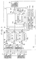
- a multiplex transmission apparatus 10 in accordance with the present invention is interconnected with other multiplex transmission apparatuses 11 via two transmission lines 20 and 21.
- three comparators 24 through 26 are connected to the transmission lines 20 and 21 via voltage converting circuits 22 and 23.
- the comparator 24 compares voltages "a” and "b” from the two transmission lines 20 and 21.
- the comparator 25 compares the voltage "a” from the transmission line 20 with a reference voltage Vc.
- the comparator 26 compares the voltage "b” from the transmission line 21 with a reference voltage Vd.
- the passive signal shown in the figure provides an input of a multiplex transmission control circuit 32 to be discussed later; in other words, it refers to a signal on the transmission line 20 or 21 where an output "i" of a logical synthesizing circuit 31 is expected to be at low level.
- the dominant signal refers to a signal on the transmission line 20 or 21 where the aforementioned output "i" is expected to be at high level.
- the signals on the transmission lines 20 and 21 are converted by voltage converting circuits 22 and 23 to output voltages a" and "b" in the states shown in FIG. 3. Further, in this embodiment, the reference voltages Vc and Vd supplied to the comparators 25 and 26 are set as shown in FIG. 3.
- the outputs "c” through “e” of the comparators 24 through 26 are supplied to differential circuits 27 through 29, respectively.
- the differential circuit 27 comprises a counter 27a and an AND gate 27b
- the differential circuit 28 comprises a counter 28a and an AND gate 28b
- the differential circuit 29 comprises a counter 29a and an AND gate 29b.
- the outputs "c” through “e” of the comparators 24 through 26 are supplied to the counters 27a, 28a, and 29a, and the AND gates 27b, 28b, and 29b.
- the counters 27a, 28a, and 29a detect whether the outputs "c” through “e” of the comparators 24 through 26 stay in the "H” state for a predetermined time, e.g., for more than T1 time.
- the counters 27a, 28a, and 29a issue “L” if the outputs "c” through “e” of the comparators 24 through 26 stay in the "H” state for more than the T1 time while they issue "H” in normal operation.
- the predetermined time T1 is longer than the longest "H” signal in a message, i.e., it is equivalent to approximately a 1/2 to 1 message length.
- the time T1 may differ among the counters 27a through 29a.
- the AND gates 27b, 28b, and 29b calculate logical products of the outputs "c" through “e” of the comparators 24 through 26 and the outputs of the counters 27a through 29a, then issue the calculation results.
- Outputs "g” and “h” of the AND gates 28b and 29b are supplied to an OR gate 30 and a signal comparing circuit 33, respectively.
- the outputs of the counters 28a and 29a are sent to a logical synthesizing circuit 31 other than the aforementioned AND gates 28b and 29b. Further, an output "f" of the AND gate 27b is supplied to the logical synthesizing circuit 31.
- the OR gate 30 supplies a logical sum of the outputs "g" and "h” of the AND gates 28b and 29b to the logical synthesizing circuit 31.
- the logical synthesizing circuit 31 of the multiplex transmission apparatus 10 is comprised of an AND gate 31a connected to the counters 28a and 29a, an AND gate 31b connected to the AND gate 27b and the AND gate 31a, counters 31c and 31d connected to the AND gate 31b, an OR gate 31e connected to the AND gate 31a and the counter 31d, an RS flip-flop 31f connected to the counter 31c and the OR gate 31e, an AND gate 31g, and an OR gate 31h connected to the AND gate 31b and the AND gate 31g.
- the AND gate 31a calculates logical products of the outputs received from the counters 28a and 29a and sends the calculation results to the AND gate 31b and the OR gate 31e.
- the AND gate 31b calculates logical products of the output "f" received from the AND gate 27b and the output received from the AND gate 31a, and sends the calculation results to the counters 31c and 31d, and the OR gate 31h.
- the counter 31c detects whether an output from the AND gate 31b stays in the "H” state for more than a predetermined time, for example, T2 time. If the output from the AND gate 31b stays in the "H” state for more than the aforementioned T2 time, then the counter 31c applies an "H" reset signal to the RS flip-flop 31f.
- the predetermined time T2 is approximately equivalent to a length of 1/2 to 10 bits.
- the counter 31d detects whether an output of the AND gate 31b stays in the "L” state for more than the aforementioned predetermined time T1. If the output of the AND gate 31b stays in the "L” state for more than the T1 time, then the counter 31d issues the "H" set signal to the OR gate 31e.
- the OR gate 31e calculates logical sums of the outputs received from the AND gate 31a and the counter 31d, and applies the reset signal, which is the calculation result, to the RS flip-flop 31f.
- the RS flip-flop 31f is reset by the reset signal received from the counter 31c, while it is set by the set signal received from the OR gate 31e, and it sends the "H" signal to the AND gate 31g.
- the AND gate 31g calculates logical products of the outputs from the OR gate 30 and the RS flip-flop 31f, and applies the calculation results to the OR gate 31h.
- the OR gate 31h calculates the logical sums of the outputs from the AND gates 31b and 31g and applies the calculation results (data) "i" to the multiplex transmission control circuit 32 and the signal comparing circuit 33.
- the multiplex transmission control circuit 32 takes in the data "i” from the OR gate 31 and controls the connected devices according to the aforementioned data "i".
- the signal comparing circuit 33 comprises a signal comparator 33a connected to the AND gate 28b and the OR gate 31h, and a signal comparator 33b connected to the AND gate 29b and the OR gate 31h.
- the signal comparator 33a compares an output "g" from the AND gate 28b with an output "i” from the OR gate 31h, and supplies the comparison result to a display circuit 34.
- the signal comparator 33b compares the output h given by the AND gate 29b with the output i given by the OR gate 31h, and supplies the comparison result to the display circuit 34.
- the display circuit 34 comprises a display 34a, which shows the comparison results (information on failures in the transmission line 20) given by the signal comparator 33a, and a display 34b which shows the comparison results (information on failures in the transmission line 21) given by the signal comparator 33b.
- the multiplex transmission apparatus 10 If the multiplex transmission apparatus 10 is in an idle state where no message is received from the transmission lines 20 and 21, that is, if the passive signal lasts for more than 1 message long, then the output "f" of the AND gate 27b will be "L” also for more than 1 message long. This causes the counter 31d to issue the set signal to set the RS flip-flop 31f. When the RS flip-flop 31f has been set and the "H" signal is issued, the AND gate 31g is opened. Then the AND gate 31g lets the logical sum of the outputs "g" and "h” of the AND gates 28b and 29b, i.e., the output of the OR gate 30, to pass.
- the AND gate 31a also issues "H”, causing the AND gate 31b to open; therefore, the output "f” of the AND gate 27b passes through the AND gate 31b. Accordingly, the logical sum of the outputs "f” through “h” is supplied as the output "i” from the OR gate 31h to the multiplex transmission control circuit 32.
- the signal comparator 33a takes the then outputs "g” and “i” from the AND gate 28b and the OR gate 31h and compares these outputs "g” and “i”.
- the signal comparator 33b also takes in the then outputs "h” and “i” from the AND gate 29b and the OR gate 31h and compares these outputs "h” and “i”. In this case, the aforementioned outputs "g” and “i”, and the outputs "h” and “i” coincide with each other, respectively; therefore, the signal comparators 33a and 33b output information, which indicates that the transmission lines 20 and 21 are normal, to the displays 34a and 34b, so that the displays 34a and 34b can indicate the aforementioned information.
- the AND gates 31a is closed by the output received from the counter 28a, and the output of the AND gate 31a becomes "L". Accordingly, the AND gate 31b is closed, the output of the OR gate 31e becomes "H", and the RS flip-flop 31f is set, causing the AND gate 31g to open. Therefore, a logical sum of the outputs g and h from the AND gates 28b and 29b appears in the output "i" of the OR gate 31h, and this output "i” is taken into the multiplex transmission control circuit 32.
- the multiplex transmission control circuit 32 detects signals on the transmission lines in accordance with the output "i" which is a comparison result of the comparators 24 through 26.
- the signal comparator 33a takes in the then outputs "g” and “i” from the AND gate 28b and the OR gate 31h and compares the outputs "g” and "i". In this case, the outputs "g” and “i” disagree; therefore, the signal comparator 33a outputs information, which indicates that the transmission line 20 has incurred a failure, to the display 34a, so that the display 34a can indicate the aforementioned information.
- the output of the AND gate 31a is "H", but the output "f" of the AND gate 27b is “L”, and therefore the output of the AND gate 31b becomes “L”. Accordingly, the output given by the counter 31d becomes “H”, and the RS flip-flop 31f is set, causing the AND gate 31g to open. Therefore, a logical sum of the outputs "f” through “h” from the AND gates 27b, 28b and 29b appears in the output "i" of the OR gate 31h, and this output "i” is taken into the multiplex transmission control circuit 32.
- the multiplex transmission control circuit 32 detects signals on the transmission lines in accordance with the output "i" which is a comparison result of the comparators 24 through 26.
- the signal comparator 33b takes in the then outputs "h” and “i” from the AND gate 29b and the OR gate 31h, and compares the outputs "h” and "i". In this case, the outputs "h” and “i” disagree; therefore, the signal comparator 33b outputs information, which indicates that the transmission line 21 has incurred a failure, to the display 34b, so that the display 34b can indicate the aforementioned information.
- the output "i" can be determined in the logical sums of the outputs "f" through “h” by following the same approach as that for the aforementioned mode 2 or 3.
- the outputs of these comparators pass through their respective differential circuits, thus automatically setting the output of the differential circuit, which is linked to a comparator connected to the faulty transmission line, to "L"
- Only normal signals are sent to the multiplex transmission control circuit by using a logical sum of the outputs of those differential circuits as the input to the multiplex transmission control circuit.
- the constants of the differential circuits are set such that the respective counters remain in "H" state for a fixed time. It is therefore possible to use an ordinary frame and thus a wide range of application is ensured.
- FIG. 4 is a configuration block diagram which shows the second embodiment of the multiplex transmission apparatus in accordance with the present invention.
- the same sections as those in the first embodiment of FIG. 1 are assigned the same signs for the convenience of explanation.
- the configuration of this multiplex transmission apparatus differs from that of the first embodiment in that the outputs of the counters 27a through 29a are supplied to an AND gate 31i of the logical synthesizing circuit 31 in addition to the sections shown in the first embodiment and that the RS flip-flop 31j of the logical synthesizing circuit 31 is set by an output of the counter 28a and reset by an output of the AND gate 31i.
- the transmission lines are connected to a bias voltage supply circuit 35 and a driving circuit 36 when the RS flip-flop 31j is set, while the transmission lines are disconnected from the bias voltage supply circuit 35 and the driving circuit 36 when the RS flip-flop 31j is reset.
- the bias voltage supply circuit 35 comprises a resistor R1 connected between the transmission line 21 and the power supply, a resistor R2 connected between the transmission line 20 and the ground, a switch 35a which is provided between the resistor R2 and the ground and which is switched by an output of the RS flip-flop 31j, and a resistor R3 connected between the transmission line 20 and the ground, and it supplies bias voltage to the transmission lines 20 and 21.
- the bias voltage of the transmission lines is adequately set to the power supply side even in the event that the transmission lines 20 and 21 are short-circuited.
- the driving circuit 36 comprises a constant-current section 36a which supplies current to the transmission line 20, a constant-current section 36b which takes in currents from the transmission line 21, a buffer 36c provided between the constant-current section 36b and the multiplex transmission control circuit 32, and a switch 36d which is switched by an output of the RS flip-flop 31j.
- the outputs "c” through “e” of the comparators 24 through 26 will be all “H” whether the signal is passive or dominant, but if the voltage supply circuit 35 and the driving circuit 36 are disconnected from the transmission lines, the outputs "c” and “d” in response to the passive signal will be “H", while the output “e” will be “L”. The outputs "c” and “e” in response to the dominant signal will be “H”, while the output "d” will be “L”.
- one of the three or more comparators remains capable of receiving even if one of the transmission lines fails, and the outputs of these comparators pass through their respective differential circuits, thus automatically setting the output of the differential circuit, which is linked to a comparator connected to the faulty transmission line, to "L".
- Only normal signals are supplied to the multiplex transmission control circuit by using a logical sum of the outputs of those differential circuits as the input to the multiplex transmission control circuit. This enables, in this embodiment, automatic receiving without depending on message receiving even if one of the transmission lines incurs a failure, thus making it possible to perform message transmission with no waste.
- message transmission is possible even if the transmission lines are short-circuited, permitting improved reliability of the apparatus.
- the present invention is not limited thereto.
- it is also possible to control the connection between the transmission line 21 and the bias voltage supply circuit 35 and the connection between the transmission line 21 and the driving circuit 36 by connecting the switch 35a of the bias voltage supply circuit 35 between the resistor R1 and the power supply and also by connecting the switch 36d of the driving circuit 36 between the constant-current section 36b and the buffer 36c.
- bias voltage supply circuit may be provided either at one point in a network or scattered at several points.
- the RS flip-flop 31j in the second embodiment is set in response to a logical sum of the outputs of the counters 27a and 28a. It is also possible to design the system so that the RS flip-flop 31f is reset when the output "c" of the comparator 24 remains “H” for approximately a one-bit length, and that the RS flip-flop 31f is set when the output "c" remains “L” for a one-byte length to one-message length. In this case, there is an effect that eliminates the need of the gates 31a, 31b, and 31e.
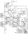
- FIG. 6 is a configuration block diagram which shows the third embodiment of the configuration of the multiplex transmission apparatus in accordance with the present invention.
- the same sections as those in the second embodiment shown in FIG. 4 are assigned the same signs for the convenience of explanation.
- the configuration of the multiplex transmission apparatus differs from that of the aforementioned second embodiment in that another condition for resetting the RS flip-flop 31j has been added.
- the outputs "f,” “g,” and “h” of the AND gates 27b through 29b are supplied to the OR gates 30 and 31l to calculate the logical sum, and a signal comparing circuit 31m compares the output signal, which has taken in the logical sum, with a signal transmitted by the multiplex transmission control circuit 32.
- the comparison result "k” and the output “j" of the AND gate 31i are input to the OR gate 31k to determine the logical sum, and this output goes through a delay circuit 31n to provide the resetting condition for the RS flip-flop 31j.
- the RS flip-flop 31j is set by the logical sum of the outputs of the counters 27a and 28a at an OR gate 31p.
- the signal comparing circuit 31m functions to securely detect the failure of the mode 8 in Table 1 mentioned above, and the delay circuit 31n functions to absorb variations in the control time for the multiplex transmission apparatuses which are interconnected via the transmission lines.
- the outputs of the counters 27a through 29a are set to "L” on condition that an "H” state which lasts longer than the longest "H” signal in a message is detected.
- the counter 31c issues an output when an "H” state approximately equivalent to a one-bit length is detected.
- the counter 31d issues an output when an "L” state which lasts significantly longer than the longest “L” signal in the message is detected. This eliminates, in this embodiment, the need of the AND gate 31b shown in FIG. 4, allowing outputs of the AND gate 27b to be directly applied to the OR gate 31h.
- short circuits between the transmission lines 20 and 21 can be securely detected and also the variations in the control time for the multiplex transmission apparatuses can be absorbed.
- FIG. 7 is the configuration block diagram of the fourth embodiment and it shows the major section of the configuration of the multiplex transmission apparatus in accordance with the present invention. Other sections of the multiplex transmission apparatus which are not shown in the figure are the same as those of the first embodiment of FIG. 1.
- the configuration of the multiplex transmission apparatus differs from that of the first embodiment in that nonreversing inputs of the first comparator 43 and the second comparator 44 are connected to the transmission line 20 via a voltage converting circuit 41, and that the voltage converting circuit 41 applies a bias voltage, which is opposite from that of a bias supply circuit 46 discussed later, to the transmission line 20 through a resistor R4 of a reverse-bias voltage supply circuit 40 which is interposed between the transmission line 20 and the voltage converting circuit 41.
- the bias supply circuit 46 has a bias resistor R6 of approximately 100 ⁇ , for example, to be connected to the transmission line 20, and a bias resistor R7 of approximately 100 ⁇ , for example, to be connected to the transmission line 21.
- the bias voltage is supplied to the ground potential of the aforementioned transmission line 20 via the bias resistor R6, while the bias voltage is supplied to the VBIA potential of approximately 5V, for example, in the aforementioned transmission line 21 via the bias resistor R7.
- the values of the resistors R4 and R5 are set for about 100k ⁇ , for example, which is adequately higher than that of the bias resistors R6 and R7 to avoid affecting the bias voltages of the transmission lines 20 and 21.
- the voltage converting circuit 41 comprises resistors R8 through R10, and these resistors R8 through R10 are set for values which are within the input voltage ranges of the first comparator 43 and the second comparator 44. For instance, when a line voltage Vcc is about 5V, the resistor R8 is set for about 100k ⁇ , the resistor R9 for about 56k ⁇ , and the resistor R10 for about 68k ⁇ .
- the voltage converting circuit 42 comprises resistors R11 through R13, and these resistors R11 through R13 are set for values which are within the input voltage ranges of the first comparator 43 and the third comparator 45. For instance, when the line voltage Vcc is about 5V, the resistor R11 is set for about 100k ⁇ , the resistor R12 for about 68K ⁇ , and the resistor R13 for about 56K ⁇ .
- Reference voltages 1 and 2 to be supplied to the second comparator 44 and the third comparator 45 are set for a value which makes it possible to detect a failure which may take place in the transmission line 20 or 21.
- This value may be, for example, about Vcc/2 if the resistors R8 through R13 constituting the voltage converting circuits 41 and 42 are set for the above-mentioned values.
- the reverse-bias voltage supply circuit 40 in accordance with this embodiment is not provided, no bias voltage is supplied, and therefore, if disconnection takes place at point D of a transmission line, the voltage values of the non-reversing inputs of the first and second comparators 43 and 44 become unstable. Likewise, if disconnection takes place at point E of the transmission line, the voltage values of the reversing inputs of the first and third comparators 43 and 45 become unstable. Thus, in this case, disconnection cannot be securely detected if the reverse-bias voltage supply circuit 40 is not provided.
- the input voltages of the first through third comparators are securely set for the opposite voltages from the bias voltage supply circuit, making it possible to detect the disconnection.
- FIG. 8 is the configuration block diagram of the fifth embodiment and it shows the major section of the configuration of the multiplex transmission apparatus in accordance with the present invention.
- the other sections of the multiplex transmission apparatus which are not shown are the same as those of the first embodiment of FIG. 1.
- Reference voltages 1 and 2 supplied to the second comparator 25 and the third comparator 26 are set for a value, approximately Vcc/2, for example, which enables detection of a failure which may occur in the transmission lines 20 or 21.
- the bias voltage supply circuit 46 has the same configuration as that of the bias voltage supply circuit shown in FIG. 7.
- the configuration of the multiplex transmission apparatus differs from that of the first embodiment in that transmitted data sent out from the multiplex transmission control circuit 32 is applied to the second constant-current driving circuit 51, and constant current is taken in through the transmission line 21. It also differs in that complement data of the transmitted data from the multiplex transmission control circuit 32 are applied to the first constant-current driving circuit 50, and constant current is discharged through the transmission line 20.
- the first constant-current driving circuit 50 comprises a transistor T1, diodes D1 through D4, and resistors R20 through R23.
- the aforementioned transistor T1, diodes D1 and D2, and the resistors R20 and R21 are decisive factors of the value of the current discharged, and the current value is determined by the voltage between the base and emitter of the transistor T1, the forward voltages of the diodes D1 and D2, and the values of the resistors R20 and R21.
- the resistors R22 and R23 are resistors limiting the base current of the aforementioned transistor T1.
- the diode D3 is a diode which prevents currents from the transmission line 20 from turning in.
- the diode D4 is a diode used to prevent delay in the switching speed of the transistor T1.
- the diode D4 functions to let currents constantly flow into the collector of the transistor T1 so that the transistor T1 no longer becomes saturated, thus preventing slowdown of switching of the transistor.
- the second constant-current driving circuit 51 comprises a transistor T2, diodes D5 through D8, and resistors R24 through R27.
- the aforementioned transistor T2, diodes D5 and D6, and resistors R24 and R25 are decisive factors of the value of currents taken in.
- the current value is determined by the voltage between the base and emitter of the transistor T2, the forward voltages of the diodes D5 and D6, and the values of the resistors R24 and R25.
- the resistors R26 and R27 are resistors which limit the base current of the transistor T2.
- the diode D7 is a diode which prevents currents from the transmission line 20 from turning in.
- the diode D8 is a diode used to prevent delay in the switching speed of the transistor T2. In other words, the diode D8 functions to let currents constantly flow into the collector of the transistor T2 so that the transistor T2 no longer becomes saturated, thus preventing slowdown of switching of the transistor.
- constant-current drive is used for the driving means of the transmission lines; therefore, even if ground potential differences occur among the multiplex transmission apparatuses, the voltage value of the transmission lines can be maintained at a constant level, making it possible to reduce undesirable radiation noises produced in the transmission lines.
- the constant-current driving circuit is not saturated, causing no slowdown in the driving speed of the constant-current driving circuit. This gives an effect of ensuring simultaneity of data.
- FIG. 9 is the configuration block diagram which shows the sixth embodiment of the configuration of the multiplex transmission apparatus in accordance with the present invention.
- the sections which are the same as those of the first embodiment of FIG. 1 and the third embodiment of FIG. 6 are assigned the same signs for the convenience of explanation.
- this configuration of the multiplex transmission apparatus differs from that of the aforementioned third embodiment in three points.
- the first point is that the apparatus has the same signal comparing circuit 33 and the display circuit 34 as in the first embodiment, and the received signal i, which is issued by the OR gate 31h and supplied to the multiplex transmission control circuit 32 and the transmitted signal l issued by the aforementioned multiplex transmission control circuit 32 are supplied to the OR gate 42 to calculate the logical sum which is applied to the signal comparators 33a and 33b.
- the second point is that a counter 31q, which receives the output "c" of the comparator 24, is installed in place of the counters 31c and 31d given in the third embodiment, comparison results (information on faults in the transmission lines) "m" and "n” of the signal comparing circuit 33 are supplied to the OR gate 31r to calculate the logical sum, the outputs of the OR gate 31r, counter 31q and AND gate 31a are supplied to the OR gate 31e, and an output of the OR gate 31e is directly applied to the AND gate 31g.
- the third point is that an output of a counter 39, which counts the outputs of the comparator 37, has been added to the condition for switches 35a and 36d to disconnect the bias voltage supply circuit 35 and the constant-current section 36a from the transmission line 20, and also an output of a counter 40, which counts the outputs of the comparator 38, has been added to the condition for a switch 36e to disconnect the constant-current section 36b from the transmission line 21.
- the signal comparing circuit 33 compares the outputs "g" and “h” of the differential circuits 28 and 29 with the received signal "i" or transmitted signal l which is an output from the OR gate 42. Accordingly, the display circuit 34 can indicate comparison results of the signal comparing sections 33a and 33b at the time of transmitting as well as receiving.
- the counter 31q outputs "L” when the output "c" of the comparator 24 holds the “H” state for longer than the T2 time (approximately 1 bit long).
- the OR gate 31e issues the "L” state signal to place the AND gate 31g in the closed state when the inputs from the aforementioned counter 31q, the AND gate 31a and the OR gate 31r are all “L”. This enables the OR gate 31h to supply the output "f" of the differential circuit 27 as the received signal "i" to the multiplex transmission control circuit 32.
- the counter 31q issues "H” when the output "c" of the comparator 24 holds the "L” state for longer than the T1 time (approximately 1/2 frame long).
- the OR gate 31e places the AND gate 31g in the open state when the input from the aforementioned counter 31q is "H”. This enables the OR gate 31h to supply the logical sum of the outputs "f", "g", and "h” of the differential circuits 27, 28, and 29 as the received signal "i" to the multiplex transmission control circuit 32.
- Predetermined reference voltages Ve and Vf applied to the comparators 37 and 38 are set for specified values to enable the counters 39 and 40 to detect overvoltage in the transmission line 20 or 21.
- the aforementioned counters 39 and 40 function to accurately judge that the transmission line 20 or 21 has recovered the normal voltage. More specifically, the counters 39 and 40 issue “L” when the outputs of the comparators 37 and 38 hold the "H” state for longer than the prescribed time, and they turn off the switch 35a of the bias voltage supply circuit 35 and the switches 36d and 36e of the constant-current sections 36a and 36b. This makes it possible, in this embodiment, to disconnect the resistor R2 of the bias voltage supply circuit 35 and the driving circuit 36 from the transmission lines 20 and 21.
- the counters 39 and 40 issue “H” when the outputs of the comparators 37 and 38 hold the “L” state for longer than the predetermined time, and turn on the aforementioned switches 35a, 36d, and 36e. This makes it possible, in this embodiment, to connect the bias voltage supply circuit 35 and the driving circuit 36 to the transmission lines 20 and 21.
- the counter 31q replaces the functions of the counters 31c and 31d, eliminating the need of the RS flip-flop 31f.
- the logical sums of the comparison results "m" and "n" of the signal comparing circuit 33 are connected the OR gate 31e, so that the AND gate 31g can be opened or closed also by information on failures in the transmission lines, permitting more reliable message transmission.
- the bias voltage supply circuit 35 and the driving circuit 36 can be isolated from the transmission lines when the transmission lines incur overvoltage, making it possible to protect the aforementioned bias voltage supply circuit 35 and the driving circuit 36.
Landscapes
- Engineering & Computer Science (AREA)
- Power Engineering (AREA)
- Computer Networks & Wireless Communication (AREA)
- Signal Processing (AREA)
- Time-Division Multiplex Systems (AREA)
- Detection And Prevention Of Errors In Transmission (AREA)
- Small-Scale Networks (AREA)
Applications Claiming Priority (6)
| Application Number | Priority Date | Filing Date | Title |
|---|---|---|---|
| JP214982/91 | 1991-08-27 | ||
| JP21498291 | 1991-08-27 | ||
| JP220105/91 | 1991-08-30 | ||
| JP22010591 | 1991-08-30 | ||
| JP31666091 | 1991-11-29 | ||
| JP316660/91 | 1991-11-29 |
Publications (3)
| Publication Number | Publication Date |
|---|---|
| EP0529602A2 true EP0529602A2 (fr) | 1993-03-03 |
| EP0529602A3 EP0529602A3 (en) | 1993-07-07 |
| EP0529602B1 EP0529602B1 (fr) | 1998-10-21 |
Family
ID=27329695
Family Applications (1)
| Application Number | Title | Priority Date | Filing Date |
|---|---|---|---|
| EP92114529A Expired - Lifetime EP0529602B1 (fr) | 1991-08-27 | 1992-08-26 | Récepteur différentiel, tolérant les défauts de lignes |
Country Status (5)
| Country | Link |
|---|---|
| US (1) | US5295132A (fr) |
| EP (1) | EP0529602B1 (fr) |
| JP (1) | JP3133490B2 (fr) |
| CA (1) | CA2076932C (fr) |
| DE (1) | DE69227349T2 (fr) |
Cited By (15)
| Publication number | Priority date | Publication date | Assignee | Title |
|---|---|---|---|---|
| FR2716060A1 (fr) * | 1994-02-08 | 1995-08-11 | Bosch Gmbh Robert | Dispositif de transmission en série de données entre au moins deux stations. |
| FR2718591A1 (fr) * | 1994-04-11 | 1995-10-13 | Daimler Benz Ag | Dispositif pour surveiller des bus bifilaires. |
| DE19503460C1 (de) * | 1995-02-03 | 1996-03-07 | Daimler Benz Ag | Fehlertolerante Endstufe für ein digitales Zweileiterbus-Datenkommunikationssystem |
| WO1996011541A3 (fr) * | 1994-10-10 | 1996-06-20 | Philips Electronics Nv | Systeme de transmission numerique insensible aux defaillances |
| WO1996042159A1 (fr) * | 1995-06-08 | 1996-12-27 | Philips Electronics N.V. | Systeme de transmission de donnees a surete integree, par l'intermediaire d'un bus differentiel |
| WO2000004684A1 (fr) * | 1998-07-16 | 2000-01-27 | Koninklijke Philips Electronics N.V. | Systeme de transmission de donnees par un bus differentiel |
| EP0827872A3 (fr) * | 1996-09-09 | 2000-04-12 | Ford Motor Company | Méthode et système pour détecter des conditions de défaut dans un réseau multiplexé |
| DE19910016A1 (de) * | 1999-03-08 | 2000-09-28 | Siemens Ag | Anordnung zur Erfassung von Impedanzstörstellen bei symmetrischen Datenübertragungsleitungen |
| EP0999675A3 (fr) * | 1998-11-03 | 2002-03-13 | STMicroelectronics GmbH | Circuit detecteur de défauts de lignes pour système de transmission de données électriques |
| EP0964549A3 (fr) * | 1998-06-12 | 2003-11-19 | STMicroelectronics GmbH | Circuit de surveillance d'un réseau de transmission |
| EP1058430A3 (fr) * | 1999-06-02 | 2003-12-10 | STMicroelectronics GmbH | Arrangement de réglage des transitions pour un système electrique de transmission de données |
| DE19826388B4 (de) * | 1998-06-12 | 2007-01-11 | Sgs-Thomson Microelectronics Gmbh | Fehlerverarbeitungsschaltung für eine Empfangsstelle eines Datenübertragungssystems |
| DE10037489B4 (de) * | 1999-04-02 | 2007-02-22 | Honda Giken Kogyo K.K. | Fehlererfassungsvorrichtung für ein Kommunikationssystem |
| DE10244186B4 (de) * | 2002-09-23 | 2008-03-06 | Infineon Technologies Ag | Empfängerschaltung für ein Gegentaktübertragungsverfahren und Verfahren zur empfängerseitigen Signalverarbeitung bei Gegentaktübertragungsverfahren |
| EP3245529A4 (fr) * | 2015-01-13 | 2018-08-22 | Sital Technology Ltd. | Système de communication insensible aux défaillances |
Families Citing this family (27)
| Publication number | Priority date | Publication date | Assignee | Title |
|---|---|---|---|---|
| US5581201A (en) * | 1994-06-30 | 1996-12-03 | Tandem Computers Incorporated | Apparatus for unit control and presence detection |
| JP3221259B2 (ja) | 1994-12-06 | 2001-10-22 | 株式会社明電舎 | バス型二重化伝送装置 |
| US6421323B1 (en) | 1994-12-23 | 2002-07-16 | Applied Digital Access, Inc. | Method and apparatus for analyzing events in a telecommunications system |
| US6480548B1 (en) * | 1997-11-17 | 2002-11-12 | Silicon Graphics, Inc. | Spacial derivative bus encoder and decoder |
| US6226330B1 (en) | 1998-07-16 | 2001-05-01 | Silicon Graphics, Inc. | Eigen-mode encoding of signals in a data group |
| KR100406968B1 (ko) * | 1999-05-21 | 2003-11-28 | 엘지전자 주식회사 | Rs-449의 선로오류 감지장치 |
| US7554829B2 (en) | 1999-07-30 | 2009-06-30 | Micron Technology, Inc. | Transmission lines for CMOS integrated circuits |
| US6775339B1 (en) | 1999-08-27 | 2004-08-10 | Silicon Graphics, Inc. | Circuit design for high-speed digital communication |
| US6417713B1 (en) | 1999-12-30 | 2002-07-09 | Silicon Graphics, Inc. | Programmable differential delay circuit with fine delay adjustment |
| US7031420B1 (en) | 1999-12-30 | 2006-04-18 | Silicon Graphics, Inc. | System and method for adaptively deskewing parallel data signals relative to a clock |
| US7333516B1 (en) | 2000-07-20 | 2008-02-19 | Silicon Graphics, Inc. | Interface for synchronous data transfer between domains clocked at different frequencies |
| US6831924B1 (en) | 2000-07-20 | 2004-12-14 | Silicon Graphics, Inc. | Variable mode bi-directional and uni-directional computer communication system |
| US6703908B1 (en) | 2000-07-20 | 2004-03-09 | Silicon Graphic, Inc. | I/O impedance controller |
| US6839856B1 (en) | 2000-07-20 | 2005-01-04 | Silicon Graphics, Inc. | Method and circuit for reliable data capture in the presence of bus-master changeovers |
| US6779072B1 (en) | 2000-07-20 | 2004-08-17 | Silicon Graphics, Inc. | Method and apparatus for accessing MMR registers distributed across a large asic |
| US7248635B1 (en) | 2000-07-20 | 2007-07-24 | Silicon Graphics, Inc. | Method and apparatus for communicating computer data from one point to another over a communications medium |
| US6681293B1 (en) | 2000-08-25 | 2004-01-20 | Silicon Graphics, Inc. | Method and cache-coherence system allowing purging of mid-level cache entries without purging lower-level cache entries |
| US7130340B1 (en) * | 2000-10-27 | 2006-10-31 | Sun Microsystems, Inc. | Noise margin self-diagnostic receiver logic |
| DE10109558C1 (de) * | 2001-02-28 | 2003-01-30 | Siemens Ag | Empfängerseitige Zusatzschaltung für den Boundary Scan bei der Datenübertragung mit differentiellen Signalen |
| KR100415818B1 (ko) | 2001-05-16 | 2004-01-24 | 삼성전자주식회사 | 세탁기 |
| US7101770B2 (en) * | 2002-01-30 | 2006-09-05 | Micron Technology, Inc. | Capacitive techniques to reduce noise in high speed interconnections |
| US7235457B2 (en) * | 2002-03-13 | 2007-06-26 | Micron Technology, Inc. | High permeability layered films to reduce noise in high speed interconnects |
| DE10250920B4 (de) * | 2002-10-31 | 2005-05-04 | Siemens Ag | Ausgabeeinheit, Empfangseinheit, Anordnung zur Datenübertragung in einem Kraftfahrzeug sowie Verfahren dazu |
| US7468618B2 (en) * | 2004-06-30 | 2008-12-23 | Finisar Corporation | Microcode-initiated high speed comparator |
| US7327167B2 (en) * | 2005-04-28 | 2008-02-05 | Silicon Graphics, Inc. | Anticipatory programmable interface pre-driver |
| JP5234374B2 (ja) * | 2011-03-02 | 2013-07-10 | 日本電気株式会社 | 差動信号伝送回路、ディスクアレイコントローラ及び差動信号伝送ケーブル |
| US10340864B2 (en) * | 2012-05-04 | 2019-07-02 | Infineon Technologies Ag | Transmitter circuit and method for controlling operation thereof |
Family Cites Families (8)
| Publication number | Priority date | Publication date | Assignee | Title |
|---|---|---|---|---|
| US4233682A (en) * | 1978-06-15 | 1980-11-11 | Sperry Corporation | Fault detection and isolation system |
| US4677627A (en) * | 1985-06-05 | 1987-06-30 | International Business Machines Corp. | Error correction scheme |
| US4792950A (en) * | 1987-06-17 | 1988-12-20 | Ford Motor Company | Multiplex wiring system |
| FR2627036B1 (fr) * | 1988-02-10 | 1990-07-27 | Peugeot | Interface de raccordement d'une partie de reception d'informations d'une station dans un systeme de transmission d'informations en differentiel, par deux fils de transmission, notamment dans un vehicule automobile |
| EP0412085B1 (fr) * | 1989-02-17 | 1994-10-12 | Robert Bosch Gmbh | Interface de reseau |
| FR2654564B1 (fr) * | 1989-11-10 | 1992-01-17 | Renault | Interface de ligne pour un reseau de transmission d'informations. |
| US5097147A (en) * | 1991-02-01 | 1992-03-17 | Tektronix, Inc. | Limited amplitude signal trigger circuit |
| US5185735A (en) * | 1991-07-10 | 1993-02-09 | Hewlett Packard Company | Lan noise monitor |
-
1992
- 1992-07-09 JP JP04182160A patent/JP3133490B2/ja not_active Expired - Fee Related
- 1992-08-25 US US07/935,536 patent/US5295132A/en not_active Expired - Fee Related
- 1992-08-26 DE DE69227349T patent/DE69227349T2/de not_active Expired - Fee Related
- 1992-08-26 CA CA002076932A patent/CA2076932C/fr not_active Expired - Fee Related
- 1992-08-26 EP EP92114529A patent/EP0529602B1/fr not_active Expired - Lifetime
Cited By (24)
| Publication number | Priority date | Publication date | Assignee | Title |
|---|---|---|---|---|
| US5696777A (en) * | 1994-02-08 | 1997-12-09 | Robert Bosch, Gmbh | Device for the serial transmission of data between at least two terminals |
| FR2716060A1 (fr) * | 1994-02-08 | 1995-08-11 | Bosch Gmbh Robert | Dispositif de transmission en série de données entre au moins deux stations. |
| FR2718591A1 (fr) * | 1994-04-11 | 1995-10-13 | Daimler Benz Ag | Dispositif pour surveiller des bus bifilaires. |
| US5898729A (en) * | 1994-10-10 | 1999-04-27 | U.S. Philips Corporation | Fault tolerant digital transmission system |
| WO1996011541A3 (fr) * | 1994-10-10 | 1996-06-20 | Philips Electronics Nv | Systeme de transmission numerique insensible aux defaillances |
| KR100396415B1 (ko) * | 1994-10-10 | 2003-11-28 | 코닌클리케 필립스 일렉트로닉스 엔.브이. | 폴트허용디지탈전송시스템 |
| EP0725513A1 (fr) | 1995-02-03 | 1996-08-07 | Daimler-Benz Aktiengesellschaft | Etage final, tolérant des fautes, pour un système digital de communication de données de configuration bus bifilaire |
| DE19503460C1 (de) * | 1995-02-03 | 1996-03-07 | Daimler Benz Ag | Fehlertolerante Endstufe für ein digitales Zweileiterbus-Datenkommunikationssystem |
| US5765031A (en) * | 1995-02-03 | 1998-06-09 | Daimler-Benz Ag | Fault tolerant output stage for digital two-conductor bus data communication system |
| US6034995A (en) * | 1995-06-08 | 2000-03-07 | U.S. Philips Corporation | System for the transmission of data via a differential bus |
| WO1996042159A1 (fr) * | 1995-06-08 | 1996-12-27 | Philips Electronics N.V. | Systeme de transmission de donnees a surete integree, par l'intermediaire d'un bus differentiel |
| EP0827872A3 (fr) * | 1996-09-09 | 2000-04-12 | Ford Motor Company | Méthode et système pour détecter des conditions de défaut dans un réseau multiplexé |
| DE19826388B4 (de) * | 1998-06-12 | 2007-01-11 | Sgs-Thomson Microelectronics Gmbh | Fehlerverarbeitungsschaltung für eine Empfangsstelle eines Datenübertragungssystems |
| EP0964549A3 (fr) * | 1998-06-12 | 2003-11-19 | STMicroelectronics GmbH | Circuit de surveillance d'un réseau de transmission |
| WO2000004684A1 (fr) * | 1998-07-16 | 2000-01-27 | Koninklijke Philips Electronics N.V. | Systeme de transmission de donnees par un bus differentiel |
| EP0999675A3 (fr) * | 1998-11-03 | 2002-03-13 | STMicroelectronics GmbH | Circuit detecteur de défauts de lignes pour système de transmission de données électriques |
| US6418550B1 (en) | 1998-11-03 | 2002-07-09 | Peter Heinrich | Line error checking circuit for an electric data transmission system |
| DE19910016A1 (de) * | 1999-03-08 | 2000-09-28 | Siemens Ag | Anordnung zur Erfassung von Impedanzstörstellen bei symmetrischen Datenübertragungsleitungen |
| DE19910016C2 (de) * | 1999-03-08 | 2001-05-10 | Siemens Ag | Anordnung zur Erfassung von Impedanzstörstellen bei symmetrischen Datenübertragungsleitungen |
| DE10037489B4 (de) * | 1999-04-02 | 2007-02-22 | Honda Giken Kogyo K.K. | Fehlererfassungsvorrichtung für ein Kommunikationssystem |
| EP1058430A3 (fr) * | 1999-06-02 | 2003-12-10 | STMicroelectronics GmbH | Arrangement de réglage des transitions pour un système electrique de transmission de données |
| DE10244186B4 (de) * | 2002-09-23 | 2008-03-06 | Infineon Technologies Ag | Empfängerschaltung für ein Gegentaktübertragungsverfahren und Verfahren zur empfängerseitigen Signalverarbeitung bei Gegentaktübertragungsverfahren |
| US7457373B2 (en) | 2002-09-23 | 2008-11-25 | Infineon Technologies Ag | Receiver circuit for a push-pull transmission method and method for receiver-end signal processing in push-pull transmission methods |
| EP3245529A4 (fr) * | 2015-01-13 | 2018-08-22 | Sital Technology Ltd. | Système de communication insensible aux défaillances |
Also Published As
| Publication number | Publication date |
|---|---|
| CA2076932A1 (fr) | 1993-02-28 |
| DE69227349T2 (de) | 1999-04-01 |
| EP0529602B1 (fr) | 1998-10-21 |
| US5295132A (en) | 1994-03-15 |
| JP3133490B2 (ja) | 2001-02-05 |
| JPH05284135A (ja) | 1993-10-29 |
| EP0529602A3 (en) | 1993-07-07 |
| CA2076932C (fr) | 1996-12-17 |
| DE69227349D1 (de) | 1998-11-26 |
Similar Documents
| Publication | Publication Date | Title |
|---|---|---|
| EP0529602A2 (fr) | Récepteur différentiel, tolérant les défauts de lignes | |
| US5321689A (en) | Multipath transmission system | |
| US5216674A (en) | Method of and device for bringing a network interface out of a sleep mode into a wake-up state | |
| US5654859A (en) | Fault tolerant power distribution system | |
| EP0010882B1 (fr) | Circuit de commutation | |
| US4178620A (en) | Three state bus driver with protection circuitry | |
| US20020178321A1 (en) | Programmable system including self locking memory circuit for a tristate data bus | |
| US4528610A (en) | Short circuit fault isolation means for electrical circuit arrangements | |
| JP3773956B2 (ja) | 差動バスを介してデータを伝送するシステム | |
| US5550804A (en) | Data bus system | |
| NL8201339A (nl) | Beschermingsketen voor een datastuurketen. | |
| US5583731A (en) | Input or output device, for programmable automatic controllers to detect an electrical fault of the channels | |
| US4939730A (en) | Auto isolation circuit for malfunctioning current loop | |
| US4685113A (en) | Driver isolating circuit for common bus-type transmission of local area network | |
| EP4206697A1 (fr) | Circuit et appareil d'auto-verrouillage et de détection, et procédé de commande | |
| EP0365435B1 (fr) | Système de transmission multicanal applicable dans une automobile | |
| EP0538473B1 (fr) | Appareil de reglage de tension dans un systeme de transmission multiplex | |
| US7421366B2 (en) | Bus station connection to a bus system for restraining means and/or sensors | |
| JPS6319097A (ja) | 線路異常監視装置 | |
| JPH03254246A (ja) | Lan用伝送システム | |
| JPS6043548B2 (ja) | デジタル出力回路の動作確認方式 | |
| JPH0424140A (ja) | 多重通信システム | |
| CA2101520A1 (fr) | Methode d'elimination des defauts de ligne pour lignes de tranmission | |
| JPH04344738A (ja) | 多重伝送方式 | |
| GB2034550A (en) | Indicating faults in solid state switching circuits |
Legal Events
| Date | Code | Title | Description |
|---|---|---|---|
| PUAI | Public reference made under article 153(3) epc to a published international application that has entered the european phase |
Free format text: ORIGINAL CODE: 0009012 |
|
| AK | Designated contracting states |
Kind code of ref document: A2 Designated state(s): DE FR GB IT |
|
| PUAL | Search report despatched |
Free format text: ORIGINAL CODE: 0009013 |
|
| AK | Designated contracting states |
Kind code of ref document: A3 Designated state(s): DE FR GB IT |
|
| 17P | Request for examination filed |
Effective date: 19931231 |
|
| 17Q | First examination report despatched |
Effective date: 19960719 |
|
| GRAG | Despatch of communication of intention to grant |
Free format text: ORIGINAL CODE: EPIDOS AGRA |
|
| GRAG | Despatch of communication of intention to grant |
Free format text: ORIGINAL CODE: EPIDOS AGRA |
|
| GRAH | Despatch of communication of intention to grant a patent |
Free format text: ORIGINAL CODE: EPIDOS IGRA |
|
| GRAH | Despatch of communication of intention to grant a patent |
Free format text: ORIGINAL CODE: EPIDOS IGRA |
|
| GRAA | (expected) grant |
Free format text: ORIGINAL CODE: 0009210 |
|
| AK | Designated contracting states |
Kind code of ref document: B1 Designated state(s): DE FR GB IT |
|
| PG25 | Lapsed in a contracting state [announced via postgrant information from national office to epo] |
Ref country code: IT Free format text: LAPSE BECAUSE OF FAILURE TO SUBMIT A TRANSLATION OF THE DESCRIPTION OR TO PAY THE FEE WITHIN THE PRESCRIBED TIME-LIMIT;WARNING: LAPSES OF ITALIAN PATENTS WITH EFFECTIVE DATE BEFORE 2007 MAY HAVE OCCURRED AT ANY TIME BEFORE 2007. THE CORRECT EFFECTIVE DATE MAY BE DIFFERENT FROM THE ONE RECORDED. Effective date: 19981021 |
|
| REF | Corresponds to: |
Ref document number: 69227349 Country of ref document: DE Date of ref document: 19981126 |
|
| ET | Fr: translation filed | ||
| PG25 | Lapsed in a contracting state [announced via postgrant information from national office to epo] |
Ref country code: GB Free format text: LAPSE BECAUSE OF NON-PAYMENT OF DUE FEES Effective date: 19990826 |
|
| PLBE | No opposition filed within time limit |
Free format text: ORIGINAL CODE: 0009261 |
|
| 26N | No opposition filed | ||
| GBPC | Gb: european patent ceased through non-payment of renewal fee |
Effective date: 19990826 |
|
| PGFP | Annual fee paid to national office [announced via postgrant information from national office to epo] |
Ref country code: FR Payment date: 20000811 Year of fee payment: 9 |
|
| PG25 | Lapsed in a contracting state [announced via postgrant information from national office to epo] |
Ref country code: FR Free format text: LAPSE BECAUSE OF NON-PAYMENT OF DUE FEES Effective date: 20020430 |
|
| REG | Reference to a national code |
Ref country code: FR Ref legal event code: ST |
|
| PGFP | Annual fee paid to national office [announced via postgrant information from national office to epo] |
Ref country code: DE Payment date: 20020904 Year of fee payment: 11 |
|
| PG25 | Lapsed in a contracting state [announced via postgrant information from national office to epo] |
Ref country code: DE Free format text: LAPSE BECAUSE OF NON-PAYMENT OF DUE FEES Effective date: 20040302 |