EP0530376B1 - Halbleiterspeicher mit nichtfluechtiger halbleiterspeicherzelle - Google Patents
Halbleiterspeicher mit nichtfluechtiger halbleiterspeicherzelle Download PDFInfo
- Publication number
- EP0530376B1 EP0530376B1 EP92907106A EP92907106A EP0530376B1 EP 0530376 B1 EP0530376 B1 EP 0530376B1 EP 92907106 A EP92907106 A EP 92907106A EP 92907106 A EP92907106 A EP 92907106A EP 0530376 B1 EP0530376 B1 EP 0530376B1
- Authority
- EP
- European Patent Office
- Prior art keywords
- semiconductor memory
- cell
- memory cell
- redundancy
- load transistor
- Prior art date
- Legal status (The legal status is an assumption and is not a legal conclusion. Google has not performed a legal analysis and makes no representation as to the accuracy of the status listed.)
- Expired - Lifetime
Links
Images


Classifications
-
- G—PHYSICS
- G11—INFORMATION STORAGE
- G11C—STATIC STORES
- G11C29/00—Checking stores for correct operation ; Subsequent repair; Testing stores during standby or offline operation
- G11C29/70—Masking faults in memories by using spares or by reconfiguring
- G11C29/78—Masking faults in memories by using spares or by reconfiguring using programmable devices
- G11C29/80—Masking faults in memories by using spares or by reconfiguring using programmable devices with improved layout
- G11C29/816—Masking faults in memories by using spares or by reconfiguring using programmable devices with improved layout for an application-specific layout
- G11C29/82—Masking faults in memories by using spares or by reconfiguring using programmable devices with improved layout for an application-specific layout for EEPROMs
-
- G—PHYSICS
- G11—INFORMATION STORAGE
- G11C—STATIC STORES
- G11C16/00—Erasable programmable read-only memories
- G11C16/02—Erasable programmable read-only memories electrically programmable
- G11C16/04—Erasable programmable read-only memories electrically programmable using variable threshold transistors, e.g. FAMOS
- G11C16/0408—Erasable programmable read-only memories electrically programmable using variable threshold transistors, e.g. FAMOS comprising cells containing floating gate transistors
- G11C16/0441—Erasable programmable read-only memories electrically programmable using variable threshold transistors, e.g. FAMOS comprising cells containing floating gate transistors comprising cells containing multiple floating gate devices, e.g. separate read-and-write FAMOS transistors with connected floating gates
-
- G—PHYSICS
- G11—INFORMATION STORAGE
- G11C—STATIC STORES
- G11C16/00—Erasable programmable read-only memories
- G11C16/02—Erasable programmable read-only memories electrically programmable
- G11C16/06—Auxiliary circuits, e.g. for writing into memory
- G11C16/10—Programming or data input circuits
-
- G—PHYSICS
- G11—INFORMATION STORAGE
- G11C—STATIC STORES
- G11C16/00—Erasable programmable read-only memories
- G11C16/02—Erasable programmable read-only memories electrically programmable
- G11C16/06—Auxiliary circuits, e.g. for writing into memory
- G11C16/26—Sensing or reading circuits; Data output circuits
-
- G—PHYSICS
- G11—INFORMATION STORAGE
- G11C—STATIC STORES
- G11C7/00—Arrangements for writing information into, or reading information out from, a digital store
- G11C7/12—Bit line control circuits, e.g. drivers, boosters, pull-up circuits, pull-down circuits, precharging circuits, equalising circuits, for bit lines
Definitions
- the present invention pertains to a semiconductor memory, such as an EPROM or an EEPROM, having a non-volatile semiconductor memory cell.
- FIG.1 is a circuit diagram of an example of a conventional non-volatile semiconductor memory, specifically showing a main part of a memory cell portion of an EPROM.
- 1 represents an EPROM cell constituting a memory cell; 2 a word line; 3 a enhancement nMOS serving as a load transistor; 4 a power line for supplying a power supply voltage Vcc of, for example, +5 [V]; 5 an amplifier; and 6 an output terminal.
- FIG.1B is a circuit diagram showing a configuration of an amplifier 5.
- the amplifier 5 of FIG.1B is an inverter constructed by a cascade connection of inverters 51 and 52. There is a feedback from a point midway between the inverters back to a PMOS transistor 53, resulting in a high-speed build-up of the circuit.
- a power supply voltage Vcc is set for the word line 2 when no electrons are injected into a charge storage gate of the EPROM cell 1, i.e. a so-called floating gate (when nothing is written thereto; in other words when a logic state of the memory is "1")
- Vcc a power supply voltage
- the EPROM cell 1 is turned ON and a current flows from the drain to the source of the EPROM cell 1.
- the level of voltage of a node 7 drops to 0 [V], which voltage is output to the output terminal 6 via the amplifier 5.
- the nMOS 3 which serves as a load transistor is designed in such a manner that the voltage of the node 7 is 0 [V] when nothing is written in the EPROM cell 1, i.e. when the logic state thereof is "1", and the voltage of the node 7 is Vcc [V] when something is written in the EPROM cell 1, i.e. when the logic state thereof is "0".
- EPROM has a disadvantage in that, despite the writing of the logic "0" into the EPROM cell 1, i.e. despite the injection of electrons into the floating gate of the EPROM cell 1, the electrons in the floating gate of the EPROM cell 1 are depleted by being heated in a subsequent assembly process or an acceleration test.
- the object of the present invention is to provide a non-volatile semiconductor memory capable of reading out an initially stored memory content even after a depletion of electrons due either to heating during an assembly process or an acceleration test or to age deterioration, the assembly process or the acceleration test being carried out subsequent to the injection of electrons into the floating gate of non-volatile semiconductor memory cells such as an EPROM cell or an EEPROM cell.
- a semiconductor memory as specified by claim 1. It comprises a non-volatile semiconductor memory cell having a charge storage gate, and a write enabled load transistor having, like the above-mentioned semiconductor memory cell, a charge storage gate, the load transistor being provided for reading the content of the above-mentioned semiconductor memory cell.
- Such a memory makes it possible to read out an initially stored memory content even after a depletion of electrons due either to heating during an assembly process or an acceleration test or to age deterioration, the assembly process or the acceleration test being carried out subsequent to the injection of electrons into the floating gate of non-volatile semiconductor memory cells such as an EPROM cell or an EEPROM cell.
- FIG.2 is a diagram depicting a main part of an embodiment of the present invention. Parts that are the same as those in FIGS. 1A and 1B are given the same reference numerals.
- the non-volatile semiconductor memory of the present invention comprises a non-volatile semiconductor memory cell 1 having a floating gate, and a load transistor 8 provided for reading the content of this semiconductor memory cell 1.
- the load transistor 8 is configured to have, like the non-volatile semiconductor memory cell 1, a floating gate, and to be write enabled.
- 2 represents a word line; 4 a power line for supplying a power supply voltage Vcc; 5 an amplifier; and 6 an output terminal.
- the amplifier 5 is configured in the same way as shown in FIG.1B.
- the injection of electrons into the floating gate of the load transistor 8 in conjunction with the injection of electrons into the floating gate of the non-volatile semiconductor memory cell 1 ensures that, as electrons are depleted from the floating gate of the semiconductor memory cell 1 due either to heating during a subsequent assembly process or an acceleration test or to age deterioration, electrons in the floating gate of the load transistor 8 are also depleted.
- FIG.1 shows an EPROM cell used as a non-volatile memory cell, this is only for the sake of convenience; a non-volatile memory cell can also be an EEPROM.
- FIG.3 is a diagram showing a write circuit of FIG.2.
- the load transistor of the EPROM cell 1 is also an EPROM cell and is given the reference numerals 8 here.
- the drain and control gate of this EPROM cell 8 are connected to the power line 4; the source thereof is connected to the drain of EPROM cell 1; the connecting point of the source of the EPROM cell 8 and the drain of the EPROM cell 1 is connected to an input terminal of the amplifier 5.
- 11 represents a write circuit of the EPROM cell 8.
- This write circuit 11 is constructed by providing a pMOS 12, a pMOS 13 and an EPROM cell 14.
- the gate of the pMOS 12 is connected to a programmable signal input terminal 15 into which a programmable signal PGM is input; the source thereof is connected to a power line 16 for supplying a write voltage Vpp of, for example, +12 [V], ; the drain thereof is connected to a control gate of the EPROM cell 14.
- the gate of the pMOS 13 is connected to the programmable signal input terminal 15; the source thereof is connected to the power line 16; the drain thereof is connected to the drain of the EPROM cell 14. Further, the floating gate of the EPROM cell 14 is connected to the floating gate of the EPROM cell 8; the source thereof is grounded.
- the write circuit 11 is designed to turn the pMOS 12, and the pMOS 13 ON by bringing the programmable signal PGM to an L level at the time of writing, supply the write voltage Vpp to the control gate and the drain of the EPROM cell 14, inject electrons into the floating gate of the EPROM cell 14, and distribute these electrons to the floating gate of the EPROM cell 18.
- the writing of the semiconductor memory cell 1 is conducted by the word line 2 via the control gate.
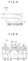
- FIG.4 is a diagram describing an effect of an embodiment of the present invention.
- the injection of electrons into the floating gate of the EPROM cell 1 takes place in conjunction with the injection of electrons into the floating gate of the EPROM cell 8. This injection ensures that, as electrons are depleted from the floating gate of the EPROM cell 1 due either to heating during a subsequent assembly process or an acceleration test or to age deterioration, electrons in the floating gate of the EPROM cell 8 are also depleted.
- the quantity of electrons injected into the floating gate of the EPROM cell 8 and the quantity of electrons injected into the floating gate of the EPROM cell 1 can either be the same as or different from each other. It is sufficient that these quantities be large enough to maintain the voltage difference Vth 8 - Vth 1 between the threshold voltage Vth 8 of the EPROM cell 8 and the threshold voltage Vth 1 of the EPROM cell 1 at the same level.
- FIG.5 is a cross-sectional view depicting a suitable structure of a load transistor of the present invention.
- 22 represents a P-type silicon substrate; 23 an N - diffused layer serving as a drain region; 24 a N + diffused layer also serving as a drain region; 25 a N - diffused layer serving as a source region; 26 a N + diffused layer also serving as a source region; 27 a floating gate; 28 a control gate; 29, 30 aluminum wirings, and 31 an insulating layer.
- the N - diffused layer 23 serving as the drain region is of a so-called LDD (Light Doped Drain) structure.
- LDD Light Doped Drain
- This LDD structure is provided in order to repress the injection of electrons into the floating gate. This repression is required because the injection of electrons into the floating gate during an operation causes such a variation of the threshold voltage Vth 8 , the variation being expected because 5 [V] is applied to the drain and gate of the EPROM cell 8.
- the initially stored memory content can be read out even after the depletion of electrons from the floating gate of the non-volatile semiconductor memory cell 1, thereby improving a retention characteristic of the memory cell (quality of electric charge retention).
- FIG.6 is a diagram depicting an application of the present invention.
- FIG.6 shows a case where the present invention is applied to a redundancy circuit of a memory address circuit in an EPROM.
- a cell array 41 comprises a sense amplifier circuit 42, a column decoder 43, and a line decoder 44.
- the sense amplifier circuit 42 receives an input of a write signal and outputs a read signal.
- Write or read address signals A 0 - A 5 are fed to the column decoder 43 via a column buffer 45.
- Write or read address signals A 6 - A n are fed to the line decoder 44 via respective line buffers 46.
- each redundancy circuit 47 For each of the address signals A 6 - A n , the write circuit 11, the memory cell portion 10, and the amplifier 5 shown in FIG.3, and a redundancy determination circuit 47 are provided. The output from each redundancy circuit 47 and the output from each line buffer 46 are fed into each individual redundancy determination circuit 48 which corresponds to each redundancy circuit and buffer.
- each individual redundancy determination circuit 48 is fed to a redundancy determination circuit 49, where a redundancy signal is output to a redundancy decoder 50 and a selection circuit 51.
- the selection circuit 51 switches the decoder 44 between operation and non-operation.
- the cell array 41 is equipped with a redundancy cell 52, and the redundancy cell 52 is selected by the redundancy decoder 50.
- a redundancy address memory circuit is comprised of the redundancy circuits 47, the individual redundancy determination circuits 48, the redundancy determination circuit 49, the redundancy decoder 50, and the redundancy cell 52.
- FIG.6 shows a case where one set of redundancy address memory circuit is provided for the cell array 41, it is also possible to provide a plurality of sets of redundancy address memory circuits.
- the cell array 41 is checked for a defective cell by an LSI tester and, in case any defect is found, each of the EPROM cells 1, 8 (see FIG.3) of the memory cell portion 10 in the relevant redundancy circuit 47 receives a write signal.
- the redundancy determination circuit 49 outputs, when the outputs from all of the individual redundancy determination circuits 48 are in agreement, a redundancy signal to activate the redundancy decoder 50 so that the redundancy cell 52 can be selected. At the same time that this selection takes place, the selection circuit 51 switches the line decoder 44 to a non-operation state.
- the initially stored memory content can be read out even after the depletion of electrons from the EPROM cells 1, 8 due either to heating during an assembly process or acceleration test or to age deterioration, thereby allowing the function of switching to a redundancy cell to be fully accomplished.
- the present invention is not limited to the above embodiment, and can be applied in any situation where it is required to retain a memory content even after a package is completed.
- the present invention can be used in a semiconductor memory capable of retaining a memory content even after heating or age deterioration of, for example, a redundancy circuit.
Landscapes
- Engineering & Computer Science (AREA)
- Microelectronics & Electronic Packaging (AREA)
- Read Only Memory (AREA)
- Semiconductor Memories (AREA)
- Non-Volatile Memory (AREA)
- For Increasing The Reliability Of Semiconductor Memories (AREA)
Claims (4)
- Halbleitervorrichtung mit:einer nichtflüchtigen Halbleiterspeicherzelle (1), die ein Ladungsspeichergate (27) hat, undeinem Lasttransistor (8), der zum Auslesen eines Speicherinhalts der Speicherzelle (1) vorgesehen ist, dadurch gekennzeichnet, daß der Lasttransistor (8), wie die Halbleiterspeicherzelle (1), ein Ladespeichergate (27) hat, in welches in Verbindung mit dem Schreiben zu dem Ladespeichergate der Halbleiterspeicherzelle (1) geschrieben wird.
- Halbleitervorrichtung nach Anspruch 1, mit:einer Schreib-Halbleiterzelle (14) zum Schreiben in den Lasttransistor (8), mit einem Ladespeichergate, welches Gate mit dem Ladespeichergate (27) des Lasttransistors (8) verbunden ist,und einer vorbestimmten Anzahl von Schreibtransistoren (12, 13) zum Liefern der Schreibspannung an die Schreib-Halbleiterspeicherzelle (14).
- Halbleitervorrichtung nach Anspruch 2, bei der der Lasttransistor (8) durch leichtes Dotieren eines Drains (23) konstruiert ist.
- Halbleitervorrichtung nach einem der Ansprüche 1 bis 3, bei der
eine vorbestimmte Anzahl der Halbleiterspeicherzellen (1) und Lasttransistoren (8) so angeordnet sind, daß sie eine Adreßspeicherschaltung bilden, insbesondere eine Redundanz-Adreßspeicherschaltung.
Applications Claiming Priority (3)
| Application Number | Priority Date | Filing Date | Title |
|---|---|---|---|
| JP3055042A JPH04289593A (ja) | 1991-03-19 | 1991-03-19 | 不揮発性半導体記憶装置 |
| JP55042/91 | 1991-03-19 | ||
| PCT/JP1992/000323 WO1992016946A1 (en) | 1991-03-19 | 1992-03-18 | Semiconductor memory having nonvolatile semiconductor memory cell |
Publications (3)
| Publication Number | Publication Date |
|---|---|
| EP0530376A1 EP0530376A1 (de) | 1993-03-10 |
| EP0530376A4 EP0530376A4 (en) | 1993-10-20 |
| EP0530376B1 true EP0530376B1 (de) | 1997-02-05 |
Family
ID=12987612
Family Applications (1)
| Application Number | Title | Priority Date | Filing Date |
|---|---|---|---|
| EP92907106A Expired - Lifetime EP0530376B1 (de) | 1991-03-19 | 1992-03-18 | Halbleiterspeicher mit nichtfluechtiger halbleiterspeicherzelle |
Country Status (6)
| Country | Link |
|---|---|
| US (1) | US5469381A (de) |
| EP (1) | EP0530376B1 (de) |
| JP (1) | JPH04289593A (de) |
| KR (1) | KR950014803B1 (de) |
| DE (1) | DE69217297D1 (de) |
| WO (1) | WO1992016946A1 (de) |
Families Citing this family (7)
| Publication number | Priority date | Publication date | Assignee | Title |
|---|---|---|---|---|
| FR2715782B1 (fr) * | 1994-01-31 | 1996-03-22 | Sgs Thomson Microelectronics | Bascule bistable non volatile programmable, à état initial prédéfini, notamment pour circuit de redondance de mémoire. |
| GB9424598D0 (en) * | 1994-12-06 | 1995-01-25 | Philips Electronics Uk Ltd | Semiconductor memory with non-volatile memory transistor |
| JP3693504B2 (ja) * | 1998-07-31 | 2005-09-07 | 富士通株式会社 | メモリデバイス |
| JP2001014840A (ja) * | 1999-06-24 | 2001-01-19 | Nec Corp | 複数ラインバッファ型メモリlsi |
| US6906962B2 (en) * | 2002-09-30 | 2005-06-14 | Agere Systems Inc. | Method for defining the initial state of static random access memory |
| JP5165980B2 (ja) * | 2007-09-25 | 2013-03-21 | シチズン時計株式会社 | 読み出し電圧発生装置 |
| JP2009301678A (ja) * | 2008-06-17 | 2009-12-24 | Sharp Corp | 半導体記憶装置、表示装置、電子機器および半導体記憶装置の製造方法 |
Citations (1)
| Publication number | Priority date | Publication date | Assignee | Title |
|---|---|---|---|---|
| JPS6323194A (ja) * | 1986-02-12 | 1988-01-30 | サタマテイツク | 液晶デイスプレイ装置用検査方法および装置 |
Family Cites Families (9)
| Publication number | Priority date | Publication date | Assignee | Title |
|---|---|---|---|---|
| IT1209227B (it) * | 1980-06-04 | 1989-07-16 | Sgs Microelettronica Spa | Cella di memoria non volatile a 'gate' flottante elettricamente alterabile. |
| JPS6048505A (ja) * | 1983-08-26 | 1985-03-16 | Hitachi Ltd | バツクラツシユ補正装置 |
| US4829203A (en) * | 1988-04-20 | 1989-05-09 | Texas Instruments Incorporated | Integrated programmable bit circuit with minimal power requirement |
| US5016217A (en) * | 1988-05-17 | 1991-05-14 | Ict International Cmos Technology, Inc. | Logic cell array using CMOS EPROM cells having reduced chip surface area |
| JP2579346B2 (ja) * | 1988-06-17 | 1997-02-05 | 川崎製鉄株式会社 | 半導体不揮発性記憶素子 |
| JP2726503B2 (ja) * | 1989-08-09 | 1998-03-11 | 川崎製鉄株式会社 | 集積回路 |
| JP2583322B2 (ja) * | 1989-10-05 | 1997-02-19 | 川崎製鉄株式会社 | プログラマブルスイッチ回路 |
| JPH0467396A (ja) * | 1990-07-02 | 1992-03-03 | Fujitsu Ltd | 半導体不揮発性記憶素子及び記憶装置 |
| JP2829156B2 (ja) * | 1991-07-25 | 1998-11-25 | 株式会社東芝 | 不揮発性半導体記憶装置の冗長回路 |
-
1991
- 1991-03-19 JP JP3055042A patent/JPH04289593A/ja active Pending
-
1992
- 1992-03-18 KR KR1019920702893A patent/KR950014803B1/ko not_active Expired - Fee Related
- 1992-03-18 WO PCT/JP1992/000323 patent/WO1992016946A1/ja not_active Ceased
- 1992-03-18 EP EP92907106A patent/EP0530376B1/de not_active Expired - Lifetime
- 1992-03-18 US US07/949,236 patent/US5469381A/en not_active Expired - Fee Related
- 1992-03-18 DE DE69217297T patent/DE69217297D1/de not_active Expired - Lifetime
Patent Citations (1)
| Publication number | Priority date | Publication date | Assignee | Title |
|---|---|---|---|---|
| JPS6323194A (ja) * | 1986-02-12 | 1988-01-30 | サタマテイツク | 液晶デイスプレイ装置用検査方法および装置 |
Also Published As
| Publication number | Publication date |
|---|---|
| KR950014803B1 (ko) | 1995-12-14 |
| WO1992016946A1 (en) | 1992-10-01 |
| JPH04289593A (ja) | 1992-10-14 |
| KR937000950A (ko) | 1993-03-16 |
| EP0530376A1 (de) | 1993-03-10 |
| DE69217297D1 (de) | 1997-03-20 |
| EP0530376A4 (en) | 1993-10-20 |
| US5469381A (en) | 1995-11-21 |
Similar Documents
| Publication | Publication Date | Title |
|---|---|---|
| US7277311B2 (en) | Flash cell fuse circuit | |
| US5311470A (en) | Data latch circuit having non-volatile memory cell | |
| KR100228453B1 (ko) | 레벨 변환 회로 | |
| US5594687A (en) | Completely complementary MOS memory cell with tunneling through the NMOS and PMOS transistors during program and erase | |
| US4514830A (en) | Defect-remediable semiconductor integrated circuit memory and spare substitution method in the same | |
| US4858194A (en) | Nonvolatile semiconductor memory device using source of a single supply voltage | |
| US4903236A (en) | Nonvolatile semiconductor memory device and a writing method therefor | |
| US6654272B2 (en) | Flash cell fuse circuit | |
| US5136541A (en) | Programmable read only memory using stacked-gate cell erasable by hole injection | |
| US5448518A (en) | Virtual ground type nonvolatile semiconductor memory device capable of simultaneously accessing two memory cells | |
| US5157281A (en) | Level-shifter circuit for integrated circuits | |
| US5327384A (en) | Flash memory | |
| US6177830B1 (en) | High voltage charge pump using standard sub 0.35 micron CMOS process | |
| US5847995A (en) | Nonvolatile semiconductor memory device having a plurality of blocks provided on a plurality of electrically isolated wells | |
| CN1229809C (zh) | 具有读取模式用的字线驱动器的闪存装置及其操作方法 | |
| US5341329A (en) | Nonvolatile semiconductor memory device capable of preventing read error caused by overerase state and method therefor | |
| US5214606A (en) | Non-volatile semiconductor memory and method for driving the same | |
| US6404680B1 (en) | Circuit to check overerasing of repair fuse cells | |
| US6515911B2 (en) | Circuit structure for providing a hierarchical decoding in semiconductor memory devices | |
| EP0530376B1 (de) | Halbleiterspeicher mit nichtfluechtiger halbleiterspeicherzelle | |
| EP0376290A2 (de) | Nichtflüchtige Halbleiterspeicheranordnung, fähig um einen durch einen Überlöschungszustand verursachten Lesefehler zu verhindern | |
| US5896317A (en) | Nonvolatile semiconductor memory device having data line dedicated to data loading | |
| US5253200A (en) | Electrically erasable and programmable read only memory using stacked-gate cell | |
| EP0427260B1 (de) | Nicht-flüchtige Speicheranordnungen | |
| EP0377841A2 (de) | Integrierte Halbleiterschaltung, fähig ein Ereignis einer fehlerhaften Wirkung wegen Störungen zu verhindern |
Legal Events
| Date | Code | Title | Description |
|---|---|---|---|
| PUAI | Public reference made under article 153(3) epc to a published international application that has entered the european phase |
Free format text: ORIGINAL CODE: 0009012 |
|
| 17P | Request for examination filed |
Effective date: 19921207 |
|
| AK | Designated contracting states |
Kind code of ref document: A1 Designated state(s): DE FR GB |
|
| A4 | Supplementary search report drawn up and despatched |
Effective date: 19930901 |
|
| AK | Designated contracting states |
Kind code of ref document: A4 Designated state(s): DE FR GB |
|
| GRAG | Despatch of communication of intention to grant |
Free format text: ORIGINAL CODE: EPIDOS AGRA |
|
| 17Q | First examination report despatched |
Effective date: 19960328 |
|
| GRAH | Despatch of communication of intention to grant a patent |
Free format text: ORIGINAL CODE: EPIDOS IGRA |
|
| GRAH | Despatch of communication of intention to grant a patent |
Free format text: ORIGINAL CODE: EPIDOS IGRA |
|
| GRAA | (expected) grant |
Free format text: ORIGINAL CODE: 0009210 |
|
| AK | Designated contracting states |
Kind code of ref document: B1 Designated state(s): DE FR GB |
|
| REF | Corresponds to: |
Ref document number: 69217297 Country of ref document: DE Date of ref document: 19970320 |
|
| PG25 | Lapsed in a contracting state [announced via postgrant information from national office to epo] |
Ref country code: DE Effective date: 19970506 |
|
| ET | Fr: translation filed | ||
| PLBE | No opposition filed within time limit |
Free format text: ORIGINAL CODE: 0009261 |
|
| 26N | No opposition filed | ||
| REG | Reference to a national code |
Ref country code: GB Ref legal event code: IF02 |
|
| PGFP | Annual fee paid to national office [announced via postgrant information from national office to epo] |
Ref country code: FR Payment date: 20050308 Year of fee payment: 14 |
|
| PGFP | Annual fee paid to national office [announced via postgrant information from national office to epo] |
Ref country code: GB Payment date: 20050316 Year of fee payment: 14 |
|
| PG25 | Lapsed in a contracting state [announced via postgrant information from national office to epo] |
Ref country code: GB Free format text: LAPSE BECAUSE OF NON-PAYMENT OF DUE FEES Effective date: 20060318 |
|
| GBPC | Gb: european patent ceased through non-payment of renewal fee |
Effective date: 20060318 |
|
| REG | Reference to a national code |
Ref country code: FR Ref legal event code: ST Effective date: 20061130 |
|
| PG25 | Lapsed in a contracting state [announced via postgrant information from national office to epo] |
Ref country code: FR Free format text: LAPSE BECAUSE OF NON-PAYMENT OF DUE FEES Effective date: 20060331 |