EP0377841A2 - Integrierte Halbleiterschaltung, fähig ein Ereignis einer fehlerhaften Wirkung wegen Störungen zu verhindern - Google Patents
Integrierte Halbleiterschaltung, fähig ein Ereignis einer fehlerhaften Wirkung wegen Störungen zu verhindernInfo
- Publication number
- EP0377841A2 EP0377841A2 EP89122917A EP89122917A EP0377841A2 EP 0377841 A2 EP0377841 A2 EP 0377841A2 EP 89122917 A EP89122917 A EP 89122917A EP 89122917 A EP89122917 A EP 89122917A EP 0377841 A2 EP0377841 A2 EP 0377841A2
- Authority
- EP
- European Patent Office
- Prior art keywords
- node
- circuit
- control signal
- wiring
- gate
- Prior art date
- Legal status (The legal status is an assumption and is not a legal conclusion. Google has not performed a legal analysis and makes no representation as to the accuracy of the status listed.)
- Granted
Links
Images



Classifications
-
- G—PHYSICS
- G11—INFORMATION STORAGE
- G11C—STATIC STORES
- G11C11/00—Digital stores characterised by the use of particular electric or magnetic storage elements; Storage elements therefor
- G11C11/21—Digital stores characterised by the use of particular electric or magnetic storage elements; Storage elements therefor using electric elements
- G11C11/34—Digital stores characterised by the use of particular electric or magnetic storage elements; Storage elements therefor using electric elements using semiconductor devices
-
- G—PHYSICS
- G11—INFORMATION STORAGE
- G11C—STATIC STORES
- G11C16/00—Erasable programmable read-only memories
- G11C16/02—Erasable programmable read-only memories electrically programmable
- G11C16/06—Auxiliary circuits, e.g. for writing into memory
- G11C16/10—Programming or data input circuits
- G11C16/12—Programming voltage switching circuits
-
- G—PHYSICS
- G11—INFORMATION STORAGE
- G11C—STATIC STORES
- G11C16/00—Erasable programmable read-only memories
- G11C16/02—Erasable programmable read-only memories electrically programmable
- G11C16/06—Auxiliary circuits, e.g. for writing into memory
- G11C16/22—Safety or protection circuits preventing unauthorised or accidental access to memory cells
- G11C16/225—Preventing erasure, programming or reading when power supply voltages are outside the required ranges
Definitions
- This invention relates to a semiconductor integrated circuit, and more particularly to a semiconductor integrated circuit capable of preventing occurrence of erroneous operation due to noise.
- write enable signal WE of active-low (that is, which becomes active at a low level) is supplied from write-in control circuit 51 to circuit block 52 as shown in Fig. 1 in view of the arrangement of the memory blocks.
- Data write-in operation is effected in circuit block 52 in response to signal WE.
- Fig. 2 shows the schematic construction of the circuit block 52 of a conventional electrically data programmable nonvolatile semiconductor memory (EPROM).
- memory cells MC1 to MCn are each formed of a memory cell transistor.
- Fig. 3 is a cross sectional view showing the construction of memory cell MC1.
- Source 72 and drain 73 formed of n+-type diffusion regions are formed in the surface area of p-type substrate 71, floating gate 74 is formed above that portion of the substrate which lies between the source and drain, and control gate 75 is formed above the floating gate.
- the film thickness of that portion of insulation film 76 which lies between substrate 71 and floating gate 74 is set to tox1 and the film thickness of that portion of insulation film 76 which lies between floating gate 74 and control gate 75 is set to tox2.
- the EPROM is a nonvolatile memory
- data programmed into memory cell MC1 can be permanently stored unless all the stored data is erased by application of ultraviolet rays.
- the "data programming” means that electrons are injected into floating gate 74 of memory cell MC1 and data of the memory cell is set to "0". That is, memory cell MC1 having data of "1" is not programmed and set in the erasing state in which no electron is injected into floating gate 74 of the memory cell MC1.
- Vcc voltage Vcc of 5 V, for example, is applied to control gate 75 to read out data stored in memory cell MC1.
- the level of a voltage applied to control gate 75 when data is programmed into data storing memory cell MC1 is different from that applied when data is read out from the memory cell.
- voltage Vcc 5 V
- voltage Vpp (12.5 V) is applied in the data programming operation. Therefore, it is necessary to provide a switching circuit for switching voltages Vcc and Vpp in addition to externally supplied power source voltages Vcc (5 V), Vpp (12.5 V) and Vss (0 V).
- Switching circuit 102 is supplied with normal data readout voltage Vcc via terminal 142 and data programming high voltage Vpp via terminal 144 and selectively supplies voltage Vcc or Vpp as voltage SW according to an programming control signal (write enable signal).
- Voltage Vpp is also supplied to programming control section 104.
- Programming control section 104 includes transistor 134 whose drain and source are respectively connected to terminal 144 and column selection gate circuit 108 and programming control buffer 132 connected to receive voltage Vpp as a power source voltage for controlling the gate voltage of transistor 134 according to programming data Din.
- Column decoder 106 decodes a column address included in the input address to output the decoded result to column selection gate circuit 108.
- Circuit 108 includes a plurality of N-channel MOS transistors and selects memory cell MC1 based on the decoded result of decoder 106.
- Row decoder 110 decodes a row address included in the input address to output the decoded result to row address buffer 112.
- Buffer 112 is supplied with voltage SW from circuit 102 as the power source voltage and supplies a voltage to control gate 75 of memory cell MC1.
- the drain and source of memory cell MC1 are respectively connected to ground voltage terminal Vss and bit line 120.
- Bit line 120 is connected to one input terminal of sense amplifier 116 via a plurality of transistors of column selection gate circuit 108.
- Sense amplifier 116 senses "1" or "0" of data stored in memory cell MC1 by comparing the potential of bit line 120 varying according to data stored in one of memory cells MC1 selected by row decoder 110 and column decoder 106 with an input reference voltage to be described later.
- Reference voltage generation circuit 122 supplies a reference voltage to sense amplifier 116.
- Circuit 122 includes dummy cell DC constructed by the same memory cell transistor as memory cell MC1, dummy bit line 118 and column selection gate circuit 114 having normally turned-on transistors of the same number as the transistors series-connected in column selection gate circuit 108.
- the level of the reference voltage is determined by turning on dummy cell DC. In order to obtain a stable reference potential, it is necessary to design the transistor characteristics of memory cell MC1 and dummy cell DC equal to each other.
- high voltage Vpp is supplied as voltage SW from power source switching circuit 102 to row address buffer circuit 112.
- high voltage Vpp is supplied from programming controlling buffer 132 to the gate of programming controlling transistor 134. If the threshold voltage of transistor 134 is Vth, a voltage of (Vpp-Vth) is supplied to the drain of memory cell MC1 via column selection gate circuit 108. Further, high voltage Vpp is supplied from row address buffer 112 to the control gate of memory cell MC1. As a result, current flows in the source-drain path of memory cell MC1, causing hot electrons to be injected into floating gate 74 to raise the threshold voltage of memory cell MC1. In this way, data is programmed into memory cell MC1.
- voltage Vcc When data is read out from memory cell MC1, voltage Vcc is supplied as voltage SW from power source switching circuit 102 to row address buffer 112. At this time, voltage Vcc is supplied from row address buffer 112 to the control gate of memory cell MC1, permitting a voltage corresponding to data stored in memory cell MC1 to be supplied to sense amplifier 116 via column selection gate circuit 108.
- a reference voltage is also supplied from reference voltage generating circuit 122 to sense amplifier 116. Then, sense amplifier 116 compares the voltage supplied from memory cell MC1 with that supplied from dummy cell DC and outputs the comparison result as readout data to the data line.
- Fig. 4 shows the construction of power source switching circuit 102 provided in circuit 52 of Fig. 2.
- MOS transistors 53 and 54 are each formed of a depletion type N-channel MOS transistor. The drains of transistors 53 and 54 are respectively connected to Vpp power source terminal 144 and Vcc power source terminal 142, and the sources thereof are commonly connected to node 23. As described before, voltage SW at node 23 is applied to the control gate of memory cell MC1 and the like. Signal SW is directly supplied to the gate of transistor 54 and to the gate of transistor 53 via potential conversion circuit 58.
- Vpp and Vcc power source voltages are selected by means of voltage switching circuit 102 in response to signal WE.
- signal WE is set at logic level "L” and an output of potential conversion circuit 58 is set to logic level "H” in the data write-in mode.
- high voltage Vpp is applied to the gate of transistor 53 to turn on the same.
- signal WE of logic level "L” is directly applied to the gate of transistor 54 to turn off the same. Therefore, high voltage Vpp is transmitted to node 23 via transistor 53, thereby applying high voltage Vpp to the control gate of memory cell MC1.
- transistor 54 is turned on and transistor 53 is turned off, causing voltage Vcc to be supplied to node 23 via transistor 54.
- voltage Vcc is applied to the control gate of memory cell MC1.
- the potentials of the drain and control gate of a memory cell designated by an address which happens to be internally set up are raised to a high potential level, causing electrons to be injected into the control gate and effecting the data write-in operation.
- a control signal whose "L” level is set as a significant potential level tends to be pulled to "L” level potential by the capacitive coupling between the wiring and the substrate in a case where the control signal of "H” level is transmitted along the wiring formed on the substrate set at the ground potential and in this case the internal circuit may be erroneously operated.
- This invention has been made in view of the above fact, and an object of this invention is to provide a semiconductor integrated circuit capable of preventing occurrence of erroneous operation due to noise.
- the semiconductor integrated circuit comprises a circuit block whose operation is controlled by a first control signal whose significant potential level is set at a ground potential; a wiring for transmitting a second control signal whose significant potential level is set at a potential level corresponding to a power source voltage., a controller for supplying the second control signal to said wiring; and an inverter provided near said circuit block, for inverting the second control signal on said wiring to obtain the first control signal and then supplying the first control signal to said circuit block.
- a semiconductor integrated circuit in which occurrence of an erroneous operation due to noise can be suppressed can be provided.
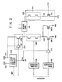
- Fig. 5 is a block diagram showing the construction of circuit block 13 (like the circuit block shown in Fig. 2) in an EPROM whose operation is controlled by write enable signal WE and to which this invention is applied.
- the significant potential level of write enable signal WE output from write-in control circuit 11 is set at "H” and the non-significant potential level thereof is set at "L”, and signal WE is transmitted to a position near circuit blocks 13 via wiring 12.
- Signal WE transmitted to the above position is then supplied to circuit blocks 13 via respective inverter circuits 14.
- each circuit block 13 Since the operation of each circuit block 13 is controlled by write enable signal WE in the same manner as in the conventional case, each circuit block 13 is set into the write-in mode when write enable signal WE output from write-in control circuit 11 is set at "H” level and set into the non-write mode when signal WE is set at "L" level. Length (L1+L2) of the wiring between write-in control circuit 11 and inverter circuit 14 is larger than length L3 between inverter circuit 14 and circuit block 13.
- Fig. 6 is a circuit diagram showing the construction of inverter circuit 14 and power source voltage switching circuit 102 arranged in a specified one of circuit blocks 13, for selecting one of power source voltage Vpp and power source voltage Vcc according to an output signal of inverter circuit 14.
- Inverter circuit 14 includes inverter 21 for inverting signal WE transmitted along wiring 12.
- CMOS transfer gate 24 is connected between output node 22 of inverter 21 and node 23 and acts as a resistor.
- Depletion type MOS transistor 25 has a source and a drain both connected to node 23 and a gate connected to power source terminal Vcc and acts as a capacitor.
- Inverter 26 inverts a signal on node 23.
- CMOS transfer gate 29 is connected between output node 27 of inverter 27 and node 28 and acts as a resistor.
- Depletion type MOS transistor 30 has a gate connected to node 28 and a source and a drain both connected to power source terminal Vss and acts as a capacitor.
- Inverter 31 inverts a signal on node 28. An output of inverter 31 is inverted by inverter 32. A signal on output node 33 of inverter 32 is supplied together with signal WE to NAND gate 34 to obtain a write-in control signal WE ′.
- power source voltage switching circuit 102 includes two depletion type N-channel MOS transistors 41 and 42 and potential converting circuit 43.
- the drains of transistors 41 and 42 are respectively connected to power source terminals Vpp and Vcc and the sources of transistors 41 and 42 are commonly connected to node 23.
- a voltage on node 23 is supplied to the control gate of memory cell MC1 in the circuit block.
- the gate of transistor 42 is supplied with output signal WE′ of AND gate 34 which is an output signal of inverter circuit 14 and the gate of transistor 41 is supplied with signal WE′ via potential converting circuit 43.
- potential converting circuit 43 functions to convert a Vcc system signal into a Vpp system signal and supplied with voltage Vpp and ground voltage Vss as a power source voltage.
- Inverter circuit 14 of the above construction functions as a delay circuit for input signal WE. That is, a signal on node 23 driven by inverter 21 is delayed by an RC delay circuit constituted by transfer gate transistor 24 and transistor 25 and supplied to inverter 26. Further, a signal on node 28 driven by inverter 26 is delayed by an RC delay circuit constituted by transfer gate transistor 29 and transistor 30 and supplied to inverter 31. Therefore, output signal WE ′ of NAND gate circuit 34 is changed from “H" level to "L” level after input signal WE is changed from "L" level to "H” level.
- output signal WE of inverter circuit 14 is varied with delay time with respect to variation in input signal WE, a filtering effect of removing noise introduced into input signal WE can be obtained.
- transistor 25 acting as a capacitor is connected between node 23 and power source terminal Vcc.
- Node 23 is a node whose potential is set to "H” level by an output signal of inverter 21 when input signal WE is in the non-significant state or at "L” level.
- the presence of transistor 25 connected between node 23 and power source terminal Vcc makes it difficult to pull the potential of node 23 to "L" level.
- transitor 30 acting as a capacitor is connected between node 28 and ground voltage terminal Vss.
- Node 28 is a node whose potential is set to "L” level by an output signal of inverter 26 when input signal WE is in the non-significant state or at "L” level.
- depletion type transistors are used as transistors 25 and 30 each acting as a capacitor in inverter circuit 14 .
- the threshold voltage thereof is negative, a channel is always formed under the gate irrespective of the potential of nodes 25 and 30, and the capacitance of the capacitor can be made larger than in the case where an enhancement type transistor is used.
- this invention is not limited to the above embodiment, and various modifications can be made.
- this invention is applied to the circuit system whose operation is controlled by a write enable signal of the EPROM.
- this invention can be applied to a circuit system whose operation can be controlled by one of various signals used in the semiconductor integrated circuit, for example, a test mode signal for effecting a stress test.
Landscapes
- Engineering & Computer Science (AREA)
- Computer Security & Cryptography (AREA)
- Computer Hardware Design (AREA)
- Read Only Memory (AREA)
- Non-Volatile Memory (AREA)
- Semiconductor Integrated Circuits (AREA)
- Semiconductor Memories (AREA)
- Logic Circuits (AREA)
- Static Random-Access Memory (AREA)
Applications Claiming Priority (2)
| Application Number | Priority Date | Filing Date | Title |
|---|---|---|---|
| JP621889A JPH088334B2 (ja) | 1989-01-13 | 1989-01-13 | 半導体集積回路 |
| JP6218/89 | 1989-01-13 |
Publications (3)
| Publication Number | Publication Date |
|---|---|
| EP0377841A2 true EP0377841A2 (de) | 1990-07-18 |
| EP0377841A3 EP0377841A3 (de) | 1991-09-18 |
| EP0377841B1 EP0377841B1 (de) | 1994-08-31 |
Family
ID=11632379
Family Applications (1)
| Application Number | Title | Priority Date | Filing Date |
|---|---|---|---|
| EP89122917A Expired - Lifetime EP0377841B1 (de) | 1989-01-13 | 1989-12-12 | Integrierte Halbleiterschaltung, fähig ein Ereignis einer fehlerhaften Wirkung wegen Störungen zu verhindern |
Country Status (4)
| Country | Link |
|---|---|
| EP (1) | EP0377841B1 (de) |
| JP (1) | JPH088334B2 (de) |
| KR (1) | KR930007184B1 (de) |
| DE (1) | DE68917896T2 (de) |
Cited By (4)
| Publication number | Priority date | Publication date | Assignee | Title |
|---|---|---|---|---|
| EP0598475A3 (de) * | 1992-11-17 | 1995-03-22 | Advanced Micro Devices Inc | Vorrichtung und Verfahren zum Schutz einer Programmierbaren logischen Schaltung gegen Überspannungen. |
| WO1996024935A1 (en) * | 1995-02-10 | 1996-08-15 | Micron Quantum Devices, Inc. | Filtered serial event controlled command port for flash memory |
| US6525967B1 (en) | 1995-02-10 | 2003-02-25 | Micron Technology, Inc. | Fast-sensing amplifier for flash memory |
| US7414454B2 (en) | 2000-10-30 | 2008-08-19 | Kabushiki Kaisha Toshiba | Voltage switching circuit |
Families Citing this family (1)
| Publication number | Priority date | Publication date | Assignee | Title |
|---|---|---|---|---|
| JP4923652B2 (ja) * | 2006-03-20 | 2012-04-25 | セイコーエプソン株式会社 | 半導体装置 |
Family Cites Families (3)
| Publication number | Priority date | Publication date | Assignee | Title |
|---|---|---|---|---|
| JPS5561357U (de) * | 1978-10-23 | 1980-04-25 | ||
| JPS63755A (ja) * | 1986-06-20 | 1988-01-05 | Fujitsu Ltd | 半導体記憶装置 |
| JPS63246843A (ja) * | 1987-04-02 | 1988-10-13 | Toshiba Corp | 半導体集積回路装置 |
-
1989
- 1989-01-13 JP JP621889A patent/JPH088334B2/ja not_active Expired - Lifetime
- 1989-12-12 EP EP89122917A patent/EP0377841B1/de not_active Expired - Lifetime
- 1989-12-12 DE DE68917896T patent/DE68917896T2/de not_active Expired - Fee Related
- 1989-12-22 KR KR1019890019287A patent/KR930007184B1/ko not_active Expired - Lifetime
Cited By (10)
| Publication number | Priority date | Publication date | Assignee | Title |
|---|---|---|---|---|
| EP0598475A3 (de) * | 1992-11-17 | 1995-03-22 | Advanced Micro Devices Inc | Vorrichtung und Verfahren zum Schutz einer Programmierbaren logischen Schaltung gegen Überspannungen. |
| WO1996024935A1 (en) * | 1995-02-10 | 1996-08-15 | Micron Quantum Devices, Inc. | Filtered serial event controlled command port for flash memory |
| US5682496A (en) * | 1995-02-10 | 1997-10-28 | Micron Quantum Devices, Inc. | Filtered serial event controlled command port for memory |
| US6525967B1 (en) | 1995-02-10 | 2003-02-25 | Micron Technology, Inc. | Fast-sensing amplifier for flash memory |
| US6578124B1 (en) | 1995-02-10 | 2003-06-10 | Micron Technology, Inc. | Serial command port method, circuit, and system including main and command clock generators to filter signals of less than a predetermined duration |
| US6581146B1 (en) | 1995-02-10 | 2003-06-17 | Micron Technology, Inc. | Serial command port method, circuit, and system including main and command clock generators to filter signals of less than a predetermined duration |
| US6744673B2 (en) | 1995-02-10 | 2004-06-01 | Micron Technology, Inc. | Feedback biasing integrated circuit |
| US6914822B2 (en) | 1995-02-10 | 2005-07-05 | Micron Technology Inc. | Read-biasing and amplifying system |
| US6996010B2 (en) | 1995-02-10 | 2006-02-07 | Micron Technology, Inc. | Fast-sensing amplifier for flash memory |
| US7414454B2 (en) | 2000-10-30 | 2008-08-19 | Kabushiki Kaisha Toshiba | Voltage switching circuit |
Also Published As
| Publication number | Publication date |
|---|---|
| DE68917896T2 (de) | 1995-02-02 |
| JPH088334B2 (ja) | 1996-01-29 |
| KR910013261A (ko) | 1991-08-08 |
| EP0377841B1 (de) | 1994-08-31 |
| DE68917896D1 (de) | 1994-10-06 |
| JPH02186666A (ja) | 1990-07-20 |
| KR930007184B1 (ko) | 1993-07-31 |
| EP0377841A3 (de) | 1991-09-18 |
Similar Documents
| Publication | Publication Date | Title |
|---|---|---|
| EP0525680B1 (de) | Zwischenspeicherschaltung für Daten mit einer nichtlöschbaren Speicherzelle | |
| US4893275A (en) | High voltage switching circuit in a nonvolatile memory | |
| US6643183B2 (en) | Channel-erase nonvolatile semiconductor memory device | |
| JP2585348B2 (ja) | 不揮発性半導体記憶装置 | |
| US5835402A (en) | Non-volatile storage for standard CMOS integrated circuits | |
| US4733371A (en) | Semiconductor memory device with high voltage switch | |
| US4866307A (en) | Integrated programmable bit circuit using single-level poly construction | |
| US6791878B2 (en) | Word line decoder in nand type flash memory device | |
| US4998223A (en) | Programmable semiconductor memory apparatus | |
| KR910007436B1 (ko) | 반도체 비휘발성 메모리 장치 | |
| US5959885A (en) | Non-volatile memory array using single poly EEPROM in standard CMOS process | |
| EP0334550B1 (de) | Nichtflüchtige RAM-Zelle | |
| EP0377840B1 (de) | Nichtflüchtige Halbleiterspeicheranordnung mit einer Referenzspannungsgeneratorschaltung | |
| US4656609A (en) | Semiconductor memory device | |
| US4910710A (en) | Input circuit incorporated in a semiconductor device | |
| EP0377841A2 (de) | Integrierte Halbleiterschaltung, fähig ein Ereignis einer fehlerhaften Wirkung wegen Störungen zu verhindern | |
| US5327392A (en) | Semiconductor integrated circuit capable of preventing occurrence of erroneous operation due to noise | |
| US5943268A (en) | Non-volatile latch having PMOS floating gate memory cells | |
| US6115293A (en) | Non-volatile semiconductor memory device | |
| US6049498A (en) | Double transistor switch for supplying multiple voltages to flash memory wordlines | |
| US5757713A (en) | Adjustable write voltage circuit for SRAMS | |
| US6639840B1 (en) | Non-volatile latch circuit that has minimal control circuitry | |
| US5896319A (en) | Current control circuit and non-volatile semiconductor memory device having the same | |
| US7768335B2 (en) | Voltage level shifter circuit | |
| JP2579346B2 (ja) | 半導体不揮発性記憶素子 |
Legal Events
| Date | Code | Title | Description |
|---|---|---|---|
| PUAI | Public reference made under article 153(3) epc to a published international application that has entered the european phase |
Free format text: ORIGINAL CODE: 0009012 |
|
| 17P | Request for examination filed |
Effective date: 19891212 |
|
| AK | Designated contracting states |
Kind code of ref document: A2 Designated state(s): DE FR GB |
|
| PUAL | Search report despatched |
Free format text: ORIGINAL CODE: 0009013 |
|
| AK | Designated contracting states |
Kind code of ref document: A3 Designated state(s): DE FR GB |
|
| 17Q | First examination report despatched |
Effective date: 19930812 |
|
| GRAA | (expected) grant |
Free format text: ORIGINAL CODE: 0009210 |
|
| AK | Designated contracting states |
Kind code of ref document: B1 Designated state(s): DE FR GB |
|
| REF | Corresponds to: |
Ref document number: 68917896 Country of ref document: DE Date of ref document: 19941006 |
|
| ET | Fr: translation filed | ||
| PLBE | No opposition filed within time limit |
Free format text: ORIGINAL CODE: 0009261 |
|
| STAA | Information on the status of an ep patent application or granted ep patent |
Free format text: STATUS: NO OPPOSITION FILED WITHIN TIME LIMIT |
|
| 26N | No opposition filed | ||
| REG | Reference to a national code |
Ref country code: GB Ref legal event code: 746 Effective date: 19980929 |
|
| REG | Reference to a national code |
Ref country code: FR Ref legal event code: D6 |
|
| REG | Reference to a national code |
Ref country code: GB Ref legal event code: IF02 |
|
| PGFP | Annual fee paid to national office [announced via postgrant information from national office to epo] |
Ref country code: GB Payment date: 20061206 Year of fee payment: 18 |
|
| PGFP | Annual fee paid to national office [announced via postgrant information from national office to epo] |
Ref country code: DE Payment date: 20061207 Year of fee payment: 18 |
|
| PGFP | Annual fee paid to national office [announced via postgrant information from national office to epo] |
Ref country code: FR Payment date: 20061208 Year of fee payment: 18 |
|
| GBPC | Gb: european patent ceased through non-payment of renewal fee |
Effective date: 20071212 |
|
| PG25 | Lapsed in a contracting state [announced via postgrant information from national office to epo] |
Ref country code: DE Free format text: LAPSE BECAUSE OF NON-PAYMENT OF DUE FEES Effective date: 20080701 |
|
| REG | Reference to a national code |
Ref country code: FR Ref legal event code: ST Effective date: 20081020 |
|
| PG25 | Lapsed in a contracting state [announced via postgrant information from national office to epo] |
Ref country code: GB Free format text: LAPSE BECAUSE OF NON-PAYMENT OF DUE FEES Effective date: 20071212 |
|
| PG25 | Lapsed in a contracting state [announced via postgrant information from national office to epo] |
Ref country code: FR Free format text: LAPSE BECAUSE OF NON-PAYMENT OF DUE FEES Effective date: 20071231 |