EP0530792B1 - Bitleitungs- und Gegenplattenfesthaltungsschaltung, insbesondere für DRAM - Google Patents
Bitleitungs- und Gegenplattenfesthaltungsschaltung, insbesondere für DRAM Download PDFInfo
- Publication number
- EP0530792B1 EP0530792B1 EP92115058A EP92115058A EP0530792B1 EP 0530792 B1 EP0530792 B1 EP 0530792B1 EP 92115058 A EP92115058 A EP 92115058A EP 92115058 A EP92115058 A EP 92115058A EP 0530792 B1 EP0530792 B1 EP 0530792B1
- Authority
- EP
- European Patent Office
- Prior art keywords
- voltage
- coupled
- node
- transistor
- precharge
- Prior art date
- Legal status (The legal status is an assumption and is not a legal conclusion. Google has not performed a legal analysis and makes no representation as to the accuracy of the status listed.)
- Expired - Lifetime
Links
Images

Classifications
-
- G—PHYSICS
- G11—INFORMATION STORAGE
- G11C—STATIC STORES
- G11C11/00—Digital stores characterised by the use of particular electric or magnetic storage elements; Storage elements therefor
- G11C11/21—Digital stores characterised by the use of particular electric or magnetic storage elements; Storage elements therefor using electric elements
- G11C11/34—Digital stores characterised by the use of particular electric or magnetic storage elements; Storage elements therefor using electric elements using semiconductor devices
- G11C11/40—Digital stores characterised by the use of particular electric or magnetic storage elements; Storage elements therefor using electric elements using semiconductor devices using transistors
- G11C11/401—Digital stores characterised by the use of particular electric or magnetic storage elements; Storage elements therefor using electric elements using semiconductor devices using transistors forming cells needing refreshing or charge regeneration, i.e. dynamic cells
- G11C11/4063—Auxiliary circuits, e.g. for addressing, decoding, driving, writing, sensing or timing
- G11C11/407—Auxiliary circuits, e.g. for addressing, decoding, driving, writing, sensing or timing for memory cells of the field-effect type
- G11C11/409—Read-write [R-W] circuits
-
- G—PHYSICS
- G11—INFORMATION STORAGE
- G11C—STATIC STORES
- G11C11/00—Digital stores characterised by the use of particular electric or magnetic storage elements; Storage elements therefor
- G11C11/21—Digital stores characterised by the use of particular electric or magnetic storage elements; Storage elements therefor using electric elements
- G11C11/34—Digital stores characterised by the use of particular electric or magnetic storage elements; Storage elements therefor using electric elements using semiconductor devices
- G11C11/40—Digital stores characterised by the use of particular electric or magnetic storage elements; Storage elements therefor using electric elements using semiconductor devices using transistors
- G11C11/401—Digital stores characterised by the use of particular electric or magnetic storage elements; Storage elements therefor using electric elements using semiconductor devices using transistors forming cells needing refreshing or charge regeneration, i.e. dynamic cells
- G11C11/4063—Auxiliary circuits, e.g. for addressing, decoding, driving, writing, sensing or timing
- G11C11/407—Auxiliary circuits, e.g. for addressing, decoding, driving, writing, sensing or timing for memory cells of the field-effect type
- G11C11/4074—Power supply or voltage generation circuits, e.g. bias voltage generators, substrate voltage generators, back-up power, power control circuits
-
- G—PHYSICS
- G11—INFORMATION STORAGE
- G11C—STATIC STORES
- G11C11/00—Digital stores characterised by the use of particular electric or magnetic storage elements; Storage elements therefor
- G11C11/21—Digital stores characterised by the use of particular electric or magnetic storage elements; Storage elements therefor using electric elements
- G11C11/34—Digital stores characterised by the use of particular electric or magnetic storage elements; Storage elements therefor using electric elements using semiconductor devices
- G11C11/40—Digital stores characterised by the use of particular electric or magnetic storage elements; Storage elements therefor using electric elements using semiconductor devices using transistors
- G11C11/401—Digital stores characterised by the use of particular electric or magnetic storage elements; Storage elements therefor using electric elements using semiconductor devices using transistors forming cells needing refreshing or charge regeneration, i.e. dynamic cells
- G11C11/4063—Auxiliary circuits, e.g. for addressing, decoding, driving, writing, sensing or timing
- G11C11/407—Auxiliary circuits, e.g. for addressing, decoding, driving, writing, sensing or timing for memory cells of the field-effect type
- G11C11/409—Read-write [R-W] circuits
- G11C11/4094—Bit-line management or control circuits
Definitions
- the present invention relates to circuits by which voltage is supplied or applied in dynamic random access memories (DRAMs), and particularly relates to (1) the bit line clamping circuit of a semiconductor memory involving the precharge or equilibration of the bit lines, and (2) a supply circuit coupled to supply an intermediate voltage supply to the capacitor plates of DRAM memory cells.
- DRAMs dynamic random access memories
- This invention is directed to DRAMs but can find application in static RAMs and other semiconductor memories as well, and other integrated circuits which have an array of memory cells disposed along orthogonal directions in a reticulated fashion, often in collections of sub-arrays. Generally, the cells are along columns defined by bit lines which are orthogonal to word lines. See , for example, Eaton, Jr. et al. U.S. Patent 4,389,715 entitled “Redundancy Scheme For A Dynamic RAM” for a general description of a DRAM, and Sud, Hardee, & Heightley U.S. Patent 4,355,377 entitled "Asynchronously Equilibrated and Pre-Charged Static RAM” for a general description of a SRAM.
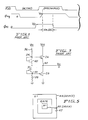
- Fig. 1 is a set of representative signals that are common in DRAMS of today's genre.
- the top waveform illustrates the row address strobe inverse signal called RAS BAR.
- RAS BAR When RAS BAR is low, the memory is in the active period, but when RAS BAR is high, the memory is in the precharge epoch. The memory alternates between such epochs many times per second.
- DRAMs are volatile and dynamic; that is, typically the data is stored in the form of a small amount of charge on a capacitor. This charge leaks away through any of a variety of mechanisms, whereupon the data becomes lost. To prevent this catastrophic result, the memory cell containing the capacitor is repeatedly read and refreshed. When it is read, a sense amplifier operates to determine what datum has been stored in the cell, and rewrites that datum in the cell. Without reading and refreshing, the data will be lost.
- the sense amplifier is generally coupled to one or a pair of bit lines which are sometimes referred to as the bit line and bit bar line.
- bit lines which are sometimes referred to as the bit line and bit bar line.
- complementary states of the data are stored in the memory cell or in a complementary pair of memory cells. Whether or not such complementary data is stored, the sensing operation, which is used during the refresh operation, involves setting the bit line which is connected to the memory cell to be refreshed to a known value. This value is commonly referred to as the "precharge voltage” or the “equilibrate voltage.”
- the equilibrate voltage causes the bit line to be precharged, and the second waveform in Fig. 1 illustrates the equilibrate voltage or signal which may be called ⁇ EQ .
- ⁇ EQ is shifted slightly to the right with respect to RAS BAR; soon after RAS BAR drops low, ⁇ EQ drops low. Also, a few nanoseconds after RAS BAR rises to the high state (Vcc), denoting the beginning of the precharge epoch, ⁇ EQ likewise rises, typically to the power supply voltage Vcc.
- Fig. 1 The restoration period normally takes several nanoseconds, and the third waveform in Fig. 1 is ⁇ RC . It will be observed that the trailing edge of ⁇ RC occurs approximately or nominally 10 nanoseconds after the rising edge of ⁇ EQ . Circuits for precharging and equilibrating the bit lines are well known.
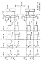
- Fig. 2 represents a prior art approach in a simplified portion of a DRAM array.
- One column includes a bit line 10a paired with a bit bar line 11a. Each of them is connected via a respective fuse 12a, 13a to a sense amplifier 14a.
- each bit line may be positioned a plurality of memory cells 15M, and, in a DRAM, a dummy cell 15D for each bit line, coupled to the sense amplifier via fuses 12, 13.
- Each memory cell 15M illustratively comprises a transistor and a capacitor. One plate of the capacitor is coupled to Vss. The other plate is coupled to the bit line via the transistor, which has a path of controllable conductivity controlled by a voltage on a word line WL.
- the word lines WL-1 to WL-N make up N rows of the array, and, as seen in Fig. 2, are orthogonal to the column (bit) lines 10, 11.
- a respective dummy memory cell 15D is included in each column, and is controlled by a dummy word line WL-D.
- the dummy cell has a capacitance that may be equal to, larger than, or smaller than that capacitance of each memory cells 15M.
- An equilibration transistor 16a has a source-drain path which couples bit lines 10a, 11a together whenever the transistor is turned on.
- the gate electrode of transistor 16a is coupled to receive the equilibration signal ⁇ EQ of Fig. 1.
- Beside transistor 16a are "keeper transistors" 18a and 20a.
- Transistor 18a has its source-drain path coupled between a line 22 and bit line 10a.
- Keeper transistor 20a has its source-drain path coupled between line 22 and bit line lla.
- the gate electrodes of transistors 18 and 20 are also coupled to receive the equilibration signal ⁇ EQ .
- transistor 16, 18 and 20 are n-channel transistors which turn on upon the application of a relatively positive voltage for ⁇ EQ , it being understood that other types of switching devices could be used, the transistors upon application of the equilibration signal ⁇ EQ equilibrate or equalize the voltages on bit lines 10a and 11a, and couple those bit lines also to receive whatever voltage is applied via line 22.
- the column circuitry of Figure 2 comprising 10a, 11a, 12a, 13a, 14a, 16a, 18a, and 20a can be referred to as columns A and A ⁇ . Further columns B and B ⁇ with identical construction are located parallel to A and A ⁇ . Indeed, a plurality of such like columns collected together in a memory chip form an array or sub-array.
- bit lines were set to either zero volts or to the power supply voltage Vcc during the precharge or equilibrate operation.
- Newer DRAMS precharge the bit lines to 1 ⁇ 2 Vcc.
- the bit and bit bar lines are typically shorted together at the beginning of the precharge cycle. (One bit line has a Vcc level and the other has a Vss level. When shorted, 1 ⁇ 2 Vcc results.)
- a voltage divider 24 can be formed from a pair of resistors, or transistors being used as resistors, coupled between Vcc and ground as illustrated in Fig. 2. The voltage obtained from the divider is then applied via line 22 to hold the bit lines near to the desired precharge value.
- a problem with precharging the bit lines to some voltage intermediate zero volts and Vcc without a separate power supply for the intermediate voltage is that the precharge voltage has a tendency to leak away during the refresh epoch and cannot be maintained in the event of a shorted bit line. If the precharge voltage does manage to dissipate entirely, the data will essentially be lost because the cell cannot be read by the sense amplifier circuit.
- fuses 12 and 13 are employed along with testing procedures to identify all such shorted bit lines.
- the bad bit lines can then be isolated from the circuit by blowing the appropriate fuse 12 (and redundant bit lines can be substituted).
- This remedy involves the addition of the fuses and the further test procedures which drive up the cost of the memory.
- One approach is reflected in EP-A2-200 500 to Chuang and Shu reflecting the preamble of claim 1. That prior art document discloses a bit line emulating circuit 72 providing a voltage targeted at 1 ⁇ 2Vcc that is applied to bit lines via a pair of transistors and further is applied to a "plate line" 47 that is common to capacitor plates in a DRAM memory array.
- circuit 72 is an on-chip VCC/2 bias generator shown in Fig. 5. Its elements seek to emulate elements of the column, and thus contains emulating capacitors 106, 112 (see page 13).
- the voltage at an output terminal 129 is determined by charge sharing between C106 and C112. Col 15, lines 8-12. Terminal 129 is connected to the input of a unity gain buffer 130 having an output that is equal to about 1 ⁇ 2VCC. Id., line 16.
- This reference therefore is not self-referencing.
- it requires a separate well and dummy memory cells which are used as "bit line emulation capacitors.”
- this approach requires extra chip area.
- Chuang et al. do not ever connect capacitor to the load to which the reference current is to be supplied.
- Taguchi EP-A2-449 310 discloses an on-chip voltage regulator.
- a regulator transistor Q1 has its gate electrode connected to node N1.
- a capacitor C is between N1 and ground.
- N1 is also connected to a gate voltage generator using constant current source I, transistors Q25-26, 29 and 30, and a clock signal CLK ⁇ .
- the source voltage of the transistor Q1 is slightly lower than the potential Vg1 of the node voltage.
- Q1 is connected to load L. However, its capacitor C is never connected to the load to which reference current is to be supplied.
- One object of the present invention accordingly, is to avoid the problem of one bad memory cell or bad bit line spoiling the entire memory. Another object is to cure the problem of bad bit lines without adding bit line fuses or the like.
- a further object of the invention is to eliminate the voltage divider used in the prior art to provide the "hold” or precharge voltage, and to avoid using the extra space required by an emulation circuit, a used in Chuang et al.
- Another object of the present invention is to decrease substantially the high standby current exhibited by the prior art.
- a worthy object of this invention is to provide a way to hold the bit lines more closely to the desired precharge voltage for an extended duration and with good control over the voltage.
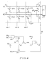
- FIG. 3 shows a four transistor power supply circuit having a first n-channel transistor 26 having a source-drain path coupled in series with the source-drain path of a first p-channel transistor 28.
- the drain of transistor 26 is coupled to Vcc, the source of transistor 26 is coupled to an output node 30, node 30 is coupled to the source of transistor 28, and the drain of transistor 28 is coupled to ground.
- a second n-channel transistor 40 has its source-drain path coupled in series with the source-drain path of a second p-channel transistor 32.
- a node 34 is coupled via a resistor 36 to a source of operating voltage, Vcc.
- Node 34 is coupled to the gate electrode and the drain of n-channel transistor 40.
- the source of transistor 40 is coupled to the source electrode of p-channel transistor 32.
- the drain of transistor 32 is coupled to ground (Vss) via a resistor 38 with a node 39 therebetween.
- the voltage developed at node 34 is 1 ⁇ 2 Vcc + Vtn.
- the voltage developed at node 39 is 1 ⁇ 2 Vcc - Vtp, where Vtn is an n-channel threshold voltage, and Vtp is a p-channel threshold voltage.
- the voltage developed at output node 30 is 1 ⁇ 2 Vcc.
- the typical 1 ⁇ 2 Vcc circuit draws considerable standby current when coupled to the cell capacitor plates.
- the 1 ⁇ 2 Vcc supply would be provided by a separate low-impedance power supply to prevent plate bounce, but the extra pin for the integrated circuit chip is undesirable. Also, it is nearly impossible to design a low-impedance intermediate value power supply "on chip" while drawing very little current from the main supplies.
- a further object of the present invention is to overcome this problem of providing an intermediate voltage to the capacitor plates of the memory cells while controlling the standby current used in that operation.
- a DRAM constructed according to the present invention does not require a voltage divider coupled to a holding node which is then coupled to keeper transistors. Rather, a device constructed according to the present invention uses a new circuit coupled to a holding line. According to claim 1 specifying the invention, the voltage holding circuit is feedback controlled.
- An apparatus of the present invention maintains the precharge voltage of the hold line, despite bit line shorts, and is further characterized by including:
- a method according to claim 12 of the present invention is characterized by including the steps of:
- the holding line is also coupled to the cell capacitor plates.
- the invented circuit and method generate a voltage that is a function of the target holding voltage.
- the "holding voltage” or “target holding voltage” means the voltage at which we desire the bit lines to be held as a result of the precharge/equilibrate operation.
- the apparatus and method Preferably generate an internal voltage (a "first voltage” or “an offset voltage”) that is simply offset from the target holding voltage by one threshold voltage transition, then held on a capacitor and later used to maintain the bit line equilibration voltage at precisely the desired holding voltage.
- logic signals are used to determine an interval during an initial portion of the precharge epoch. During that interval, transistors are turned on to generate the desired holding voltage on the holding line. Preferably this involves producing a voltage at an internal node of the circuit which is one transition voltage above the target holding voltage, and then dropping that voltage by one threshold voltage in applying it to the holding line coupled to the bit lines via keeper transistors. Meanwhile, the voltage from the internal node is also stored on the capacitor.
- the capacitor and transistors are coupled in a manner to minimize the time decay of the voltage stored on the capacitor. This is achieved in the preferred embodiment by making the capacitor fairly large and by maximizing the ratio of the capacitance to the junction area on the transistor(s) to which the capacitor is coupled in the new circuit.
- the voltage on the storage capacitor persists even after the logic signals have concluded so that during the remainder of the precharge epoch, a large drive transistor is controlled by the stored voltage.
- the drive transistor is coupled between the power supply and the holding line and thereby to the bit lines. Because of its large size, any shorts in an individual bit line, or in a number of the bit lines, will not pull the precharge voltage down to zero for all bit lines, but will be a relatively insignificant disturbance, whereby the short in a limited number of bit lines can be tolerated.
- the precharge voltage persists for a long duration, much longer than the refresh times normally specified for a DRAM.
- An alternative embodiment of the invention is that the internal node where the offset voltage is developed is decoupled from the bit lines.
- the internal node need not be permanently coupled to the capacitor, but could be selectively coupled to it so that in some manner, the voltage stored on the capacitor is preserved by decoupling the capacitor from the hold line and from other routes by which the stored charge can dissipate.
- FIG. 4 A circuit in accordance with some teachings of the present invention is illustrated in Fig. 4 which is similar in many respects to Fig. 2. Like parts have like reference numerals.
- a pair of bit lines 10, 11, with a sense amplifier 14 coupled thereto is configured with equilibration transistor 16 and transistors 18 and 20, as described above in respect of Fig. 2.
- the equilibration signal ⁇ EQ is applied to the gate electrodes of these equilibration and keeper transistors.
- a plurality of memory cells is coupled to each of the bit lines 10, 11. Dummy cells also may be coupled to the bit lines 10, 11. For convenience, only one pair of bit lines has been shown, but it will be understood that an entire array having plural bit line pairs is intended but not illustrated. Also it will be understood that appropriate decoders for columns and rows are to be included, as are I/O buffers, data buffers, and other peripheral circuitry common to DRAMs, as in USPN 4,389,715.
- the keeper transistors are coupled to a line (node 22) which in the circuit of Fig. 2 was coupled to a voltage divider but which in the embodiment illustrated in Fig. 4 is applied to a new circuit 40.
- the voltage which is impressed or applied by circuit 40 onto line 22 may be referred to as the "hold voltage" V h .
- line 22 is coupled to the cell capacitor plates, as well as to transistors 18, 20.
- lines 22* are coupled to line 22 and are coupled to the bottom capacitor plates of all the memory cells. It will be appreciated that lines 22* may be laid out parallel to the bit lines, or parallel to the word lines. Modification is possible in that a first line 22* may be connected to all of the bottom capacitor plates in one or more rows of memory cells, or, alternatively, to the bottom capacitor plates in one or more columns. It is noteworthy that the cell capacitor plate electrodes are coupled to the keeper transistors, which is a feature of the present invention. That is to say, providing a supply circuit 40 coupled to a line 22 which provides power to both the cell capacitor plates and to the bit lines is one of the aspects of the present invention.
- the capacitor plates may be coupled to circuit 40 without coupling circuit 40 to the bit lines.
- the circuit 40 may be coupled to the bit lines without coupling it to the capacitor plates.
- circuit 40 is coupled to both the bit lines and to the cell capacitor plates.
- bit line capacitance is being used to establish a low impedance plate voltage.
- capacitive divider current is used to effectively obtain a low impedance plate supply without the necessity of adding an external supply and its associated pin.
- circuit 40 in Fig. 4 within circuit 40 is a logic circuit 42 taking the form illustratively of an AND gate which provides a signal during the precharge epoch. This is conveniently done by ANDing the signals ⁇ EQ and ⁇ RC which, as can be observed in Fig. 1, are commonly high for a duration of approximately 10 nanoseconds in an early or beginning portion of the precharge epoch. It will be understood that other logic circuits could be used in an application of the present invention to produce a signal which is high during an initial portion of the precharge epoch. Moreover, other circuit variations are possible which do not need to generate a separate timing signal.
- first and second switching devices 44 and 46 are coupled together to have a first node 45 between paths of controllable conductivity of the devices, coupled in series.
- these transistors take the form of n-channel field effect transistors (FETs), although other types of controllable switching devices can be used.
- the source electrode of FET 46 is coupled to a source of operating voltage (Vcc).
- the drain electrode of FET 46 is coupled to first node 45, which is coupled to the source of FET 44.
- the drain of FET 44 is coupled to a second node 47, which is coupled to the source and the gate electrode of a third transistor 48.
- the output of AND gate 42 is coupled to the control (gate) electrodes of FETs 44 and 46, and when the output of AND gate 42 goes high, it turns on these first and second transistors 44 and 46.
- the source-drain paths of transistors 44 and 46 couple first node 45 and second node 47 to Vcc.
- Transistors 44 and 46 form a load so that a voltage intermediate ground and Vcc develops at first and second nodes 45 and 47.
- second node 47 is coupled to third transistor 48, illustratively an n-channel FET.
- the drain voltage is one (n-channel) voltage transition V T below the source voltage.
- the drain of transistor 48 is coupled to the hold line 22.
- transistor 50 is coupled between Vcc and hold line 22. Its gate electrode is coupled to node 45.
- transistor 50 is a FET and may be referred to as a drive transistor.
- the voltage coupled via drive transistor 50 to hold line 22 is a function of the gate voltage, among other factors discussed infra .
- Node 45 is coupled also to one plate of a capacitor 52.
- the other plate of capacitor 52 is coupled to ground so that capacitor 52, barring leakage, stores the voltage that appears at node 45.
- a voltage develops at node 45, as mentioned, which is one voltage transition above the hold voltage. This is sufficient to turn on n-channel drive transistor 50.
- an n-channel FET is turned ON when its gate voltage is at least one V T higher than its source voltage.
- the source voltage is, by definition, the holding voltage V h .
- the voltage developed on node 45 is exactly one V T above V h . Therefore, transistor 50 is ON, and its source-drain path is conductive, so that the power supply voltage Vcc is coupled via transistor 50 to line 22.
- the next event to occur is that the restore complete signal ⁇ RC drops low. This causes the logic gate 42 to output 0 volts, which is lower than the source voltages on transistors 44 and 46 which consequently turn off.
- the hold line, FET 48, and node 47 are decoupled from node 45.
- transistor 46 turned off Vcc is also decoupled from capacitor 52.
- the voltage at node 45, V h + V T remains on capacitor 52 and continues to be supplied to the gate electrode of transistor 50.
- the equilibrate signal ⁇ EQ remains high for the remainder of the precharge epoch, so that transistors 16, 18 and 20 associated with the bit lines remain turned on.
- the bit lines have a fair number of n+ junctions and diffusions and inherently leak quickly.
- transistor 50 is constructed fairly large, illustratively having a width of 75 microns and a length of 1 micron, so that it can overcome a reasonable number of shorts in the bit lines.
- the voltage applied to line 22 by transistor 50 alone, without transistors 44 and 46 being on, should preferably be the holding voltage, defined earlier.
- the present circuit continues to apply that very same voltage to line 22 even after logic gate 42 goes low.
- the voltage stored into capacitor 52 will remain on node 45, barring leakage.
- This voltage of node 45 is V h + V T .
- transistor 50 turns on, because the gate voltage will be more than one V T above it. This couples Vcc to line 22 and the voltage thereon will begin to rise.
- Transistor 50 turns off when the voltage it impresses on line 22 rises above V h -- because the gate voltage is precisely V h + V T and the gate voltage will no longer exceed the drain voltage by one V T .
- capacitor 52 is coupled to only three places: the gate electrode (which does not draw current) of the drive transistor, and to source electrodes of transistors 44 and 46, both of which are turned off while the voltage on capacitor 52 is to be preserved (during the latter portion of the precharge epoch).
- Transistor 44 has a layout which minimizes its junction area, as illustrated in Fig. 5. It thereby maximizes the ratio of the capacitance 52 to the junction area of transistor 44. This is done illustratively by a square layout. Capacitor 52 may illustratively have 10 picofarads. There may be about 1 square micron of junction area on transistor 44. This will allow a substantial time interval before the voltage on capacitor 52 leaks away to the substrate through the junction of transistor 44. Accordingly, the voltage on capacitor 52 is conserved, remaining high through the precharge period to control the gate voltage at transistor 50. Transistor 46 can be similarly constructed.
- transistor 50 is huge in comparison to the size of any of the keeper transistors 18 or 20, so that even if there is a short on the bit line corresponding to one of the keeper transistors, there will be little damage by virtue of that short being coupled via the corresponding keeper transistor to node or line 22.
- circuit 40 is shown at the top with a further circuit 60 below.
- Circuit 60 is nearly a mirror image of circuit 40.
- circuit 40 includes n-channel transistors 44, 46, 48, and 50
- circuit 60 includes transistors 64, 66, 68, and 70, of which transistors 68 and 70 are preferably p-channel transistors.
- Hold line 22 is coupled to transistors 68 and 70.
- circuit 60 includes a capacitor 72.
- One plate of capacitor 72 is coupled to a node 65, which is also coupled to the gate electrode of transistor 70 and to the source-drain paths of transistors 64 and 66.
- a voltage Vh - Vtp develops at node 65.
Landscapes
- Engineering & Computer Science (AREA)
- Microelectronics & Electronic Packaging (AREA)
- Computer Hardware Design (AREA)
- Dram (AREA)
Claims (14)
- Speicher in der Technik eines integrierten Schaltkreises, der eine Vielzahl von Bit-Leitungen (10, 11) in Anordnung eines Speichers, wobei eine Vielzahl von Speicherzellen (15) entlang jeder Bit-Leitung angeordnet ist, sowie eine Reihe von Leseverstärkern (14) für die Anordnung besitzt, die mit diesen Leitungen verbunden sind, wobei die Bit-Leitungen über eine Gleichgewicht/Vorlade-Einrichtung (16, 18, 20) ins Gleichgewicht gebracht und vorgeladen werden, die Vorladetransistoren (18, 20) aufweist, die zwischen den Bit-Leitungen und einer Halte-Leitung (22) liegen, wobei die Halte-Leitung mit einer Spannungshaltestufe verbunden ist, dadurch gekennzeichnet, daß die Spannungshaltestufe (40) rückkopplungsgesteuert ist und eine Zielhaltespannung für die Halte-Leitung liefert, um die Vorladespannung ungeachtet von Kurzschlüssen auf den Bit-Leitungen aufrecht zu erhalten, wobei die Spannungshaltestufe (40) enthält:eine erste Einrichtung (42, 44, 46, 48), die mit der Halte-Leitung (22) verbunden ist, um davon eine Zielhaltespannung zu erhalten und eine erste mit dieser Spannung in Beziehung stehende Spannung an einem ersten Knotenpunkt (45) zu entwickeln, wobei die erste Einrichtung einen ersten Transistor (48) aufweist, der schaltungsmäßig mit der Halte-Leitung (22) und dem ersten Knotenpunkt (45) verbunden ist;eine Speichereinrichtung (52), die mit dem ersten Knotenpunkt verbunden ist, um die erste Spannung zu speichern; undeine zweite Einrichtung, die zwischen der Halte-Leitung (22) und einer Spannungsquelle (Vcc) liegt, wobei die zweite Einrichtung einen Treibertransistor (50) aufweist, der viel größer als die Vorladetransistoren ist, so daß während eines Vorladeintervalls des Speichers und ungeachtet von Kurzschlüssen in den Bit-Leitungen (10, 11) der Treibertransistor (50) die Vorladespannung auf der Halte-Leitung (22) halten kann, nachdem die erste Einrichtung die Zielhaltespannung erhält, wobei der Treibertransistor (50) so angeschlossen ist, daß er von der Speichereinrichtung gesteuert wird, um die Zielhaltespannung aufrecht zu erhalten.
- Schaltkreis gemäß Anspruch 1, wobei die erste Einrichtung eine Taktgebereinrichtung (42) sowie einen zweiten Transistor (46) aufweist, der so angeschlossen ist, daß er von der Taktgebereinrichtung gesteuert wird.
- Schaltkreis gemäß Anspruch 2, wobei die Taktgebereinrichtung eine Logikstufe (42) aufweist, die so angeschlossen ist, um an ihren Eingängen ein Gleichgewichtssignal (Φeq) sowie ein weiteres Signal (Φrc) zu empfangen.
- Schaltkreis gemäß Anspruch 2 oder 3, wobei der zweite Transistor (46) zwischen einer Quelle der Betriebsspannung (Vcc) und dem ersten Knotenpunkt (45) liegt.
- Schaltkreis gemäß irgendeinem der bisherigen Ansprüche, wobei die erste Einrichtung weiters einen dritten Transistor (44) aufweist, der so angeschlossen ist, daß er von der Taktgeberstufe gesteuert wird.
- Schaltkreis gemäß irgendeinem der bisherigen Ansprüche, wobei die erste Einrichtung einen Transistor (44) aufweist, der so angeschlossen ist, um den ersten Knotenpunkt (45) wahlweise von der Halte-Leitung zu trennen.
- Schaltkreis gemäß irgendeinem der bisherigen Ansprüche, wobei die Speichereinrichtung einen Kondensator (52) aufweist.
- Schaltkreis gemäß irgendeinem der bisherigen Ansprüche, wobei die erste Einrichtung veranlaßt, daß die Speichereinrichtung zu ausgewählten Zeiten mit der Halte-Leitung (22) verbunden und zu anderen Zeiten von der Halte-Leitung getrennt wird.
- Schaltkreis gemäß irgendeinem der bisherigen Ansprüche, wobei die erste Einrichtung enthält:einen ersten, zweiten und dritten Transistor (48, 46, 44), die Strecken mit steuerbarer Leitfähigkeit besitzen, wobei der erste und dritte Transistor in Serie zwischen dem ersten Knotenpunkt und der Halte-Leitung (22) liegen, wobei der erste Transistor mit dem dritten Transistor an einem zweiten Knotenpunkt (47) verbunden ist;eine Einrichtung (42), um ein Taktsignal zu empfangen, das mit dem Vorladeintervall in Beziehung steht;zumindest ein Transistor des ersten, zweiten und dritten Transistors so angeschlossen ist, daß er von der Einrichtung (42) gesteuert wird, um das Taktsignal zu empfangen;der erste Knotenpunkt (45) zumindest einem Transistor des ersten, zweiten und dritten Transistors zugeordnet ist, wobei der erste Knotenpunkt mit der Speichereinrichtung (52) sowie einer Steuerelektrode des Treibertransistors (50) verbunden ist;der dritte Transistor (44) so angeschlossen ist, um den ersten Knotenpunkt wahlweise von der Halte-Leitung zu trennen.
- Schaltkreis gemäß Anspruch 9, wobei der erste Transistor (48) eine Spannungsdifferenz von einer Schwellwertspannung zwischen dem zweiten Knotenpunkt (47) und der Halte-Leitung aufrecht erhält.
- Schaltkreis gemäß irgendeinem der bisherigen Ansprüche, wobei die Spannungshaltestufe weiters enthält:eine dritte Einrichtung (64-68), die mit der Halte-Leitung (22) verbunden ist, um von ihr die Zielhaltespannung zu erhalten und an einem dritten Knotenpunkt (65) eine zweite Spannung zu entwickeln, die mit dieser Spannung in Beziehung steht, wobei die dritte Einrichtung einen vierten Transistor (68) aufweist, der schaltungsmäßig mit der Halte-Leitung (22) und dem dritten Knotenpunkt (65) verbunden ist;eine weitere Speichereinrichtung (72), die mit dem dritten Knotenpunkt (65) verbunden ist, um die zweite Spannung zu speichern; undeine vierte Einrichtung, die zwischen der Halte-Leitung (22) und einer Spannungsquelle (Vss) liegt, wobei die vierte Einrichtung einen weiteren Treibertransistor (70) besitzt, der viel größer als die Vorladetransistoren ist, so daß während des Vorladeintervalls des Speichers und ungeachtet von Kurzschlüssen in den Bit-Leitungen (10, 11) der zweite Treibertransistor (70) die Vorladespannung auf der Halte-Leitung (22) aufrecht erhalten kann, nachdem die dritte Einrichtung die Zielspannung erhält, wobei der weitere Treibertransistor (70) so angeschlossen ist, daß er von der weiteren Speichereinrichtung gesteuert wird, um dadurch die Zielhaltespannung aufrecht zu erhalten, und wobei der Treibertransistor (50) der zweiten Einrichtung von einer Kanalart ist, und wobei der Treibertransistor (70) der vierten Einrichtung von der entgegengesetzten Kanalart ist.
- Verfahren zum Betreiben eines Speichers in der Technik eines integrierten Schaltkreises, der eine Vielzahl von Bit-Leitungen (10, 11) in Anordnung eines Speichers, wobei eine Vielzahl von Speicherzellen (15) entlang jeder Bit-Leitung angeordnet ist, sowie eine Reihe von Leseverstärkern (14) für die Anordnung besitzt, die mit diesen Leitungen verbunden sind, wobei die Bit-Leitungen über eine Gleichgewicht/Vorlade-Einrichtung (16, 18, 20) ins Gleichgewicht gebracht und vorgeladen werden, die Vorladetransistoren (18, 20) aufweist, die zwischen den Bit-Leitungen und einer Halte-Leitung (22) liegen, wobei die Halte-Leitung mit einer Haltespannungsstufe verbunden ist, wobei zum Aufrechterhalten der Spannung auf den Bit-Leitungen während des Vorladens das Verfahren dadurch gekennzeichnet ist, daß es in einem rückkopplungsgeregelten Betrieb eine Zielhaltespannung für die Halte-Leitung liefert, um die Vorladespannung ungeachtet von Kurzschlüssen auf den Bit-Leitungen aufrecht zu erhalten, wobei das Verfahren folgende Schritte enthält:Empfangen einer Zielhaltespannung unter Verwendung einer Einrichtung (48), die mit der Halte-Leitung (22) verbunden ist, und Entwickeln einer Spannung an einem ersten Knotenpunkt (45), die von der Zielhaltespannung versetzt ist;Speichern der Versetzungsspannung in einer Speichereinrichtung (52);Steuern eines Treibertransistors (50) , der wesentlich größer als die Vorladetransistoren ist, um von einer Spannungsquelle (Vcc) an die Halte-Leitung (22) in Übereinstimmung mit dem Verhältnis der in der Speichereinrichtung (52) gespeicherten Versetzungsspannung zur Spannung auf der Halte-Leitung eine Spannung anzulegen, um dadurch die Zielhaltespannung an der Halte-Leitung aufrecht zu erhalten.
- Verfahren gemäß Anspruch 12, wobei der Empfangs- und Entwicklungsschritt während des Vorladeintervalls des Speichers auftritt, und wobei die Schritte enthalten:Empfangen einer Zielspannung von der Halte-Leitung (22) im Zusammenhang mit dem ins Gleichgewicht bringen der Paare von Bit-Leitungen;Entwickeln der Versetzungsspannung am ersten Knotenpunkt (45) einschließlich des wahlweisen Anlegens des ersten Knotenpunkts (45) an eine Spannungsquelle (Vcc);und wobei der Speicherschritt das Speichern der Spannung am ersten Knotenpunkt in einem Kondensator und das darauffolgende Trennen des Kondensators (52) von der Halte-Leitung (22) enthält, so daß der Kondensator von den Auswirkungen von Kurzschlüssen auf irgendeiner Bit-Leitung getrennt ist.
- Verfahren gemäß Anspruch 12, wobei das Verfahren weiters das Erzeugen einer zweiten Spannung, die von der Zielhaltespannung versetzt ist; das Speichern der zweiten Versetzungsspannung in einem zweiten Kondensator; das wahlweise Trennen des zweiten Kondensators von der Halte-Leitung; das Inbetriebsetzen eines zweiten Treibertransistors in Übereinstimmung mit der zweiten Versetzungsspannung, um dadurch die Zielhaltespannung aufrecht zu erhalten; sowie das Verbinden des zweiten Treibertransistors mit den Bit-Leitungen während des Vorladens enthält.
Applications Claiming Priority (2)
| Application Number | Priority Date | Filing Date | Title |
|---|---|---|---|
| US755111 | 1985-07-15 | ||
| US07/755,111 US5253205A (en) | 1991-09-05 | 1991-09-05 | Bit line and cell plate clamp circuit for a DRAM |
Publications (3)
| Publication Number | Publication Date |
|---|---|
| EP0530792A2 EP0530792A2 (de) | 1993-03-10 |
| EP0530792A3 EP0530792A3 (en) | 1993-08-11 |
| EP0530792B1 true EP0530792B1 (de) | 1997-10-08 |
Family
ID=25037770
Family Applications (1)
| Application Number | Title | Priority Date | Filing Date |
|---|---|---|---|
| EP92115058A Expired - Lifetime EP0530792B1 (de) | 1991-09-05 | 1992-09-03 | Bitleitungs- und Gegenplattenfesthaltungsschaltung, insbesondere für DRAM |
Country Status (5)
| Country | Link |
|---|---|
| US (1) | US5253205A (de) |
| EP (1) | EP0530792B1 (de) |
| JP (1) | JP2995370B2 (de) |
| KR (1) | KR100281725B1 (de) |
| DE (1) | DE69222606T2 (de) |
Families Citing this family (19)
| Publication number | Priority date | Publication date | Assignee | Title |
|---|---|---|---|---|
| JP3712083B2 (ja) * | 1995-11-28 | 2005-11-02 | 株式会社ルネサステクノロジ | 内部電源電位供給回路及び半導体装置 |
| JPH05342873A (ja) * | 1992-06-10 | 1993-12-24 | Nec Corp | 半導体記憶装置 |
| US5317212A (en) * | 1993-03-19 | 1994-05-31 | Wahlstrom Sven E | Dynamic control of configurable logic |
| US5508962A (en) * | 1994-06-29 | 1996-04-16 | Texas Instruments Incorporated | Apparatus and method for an active field plate bias generator |
| JP2576425B2 (ja) * | 1994-10-27 | 1997-01-29 | 日本電気株式会社 | 強誘電体メモリ装置 |
| TW306001B (de) * | 1995-02-08 | 1997-05-21 | Matsushita Electric Industrial Co Ltd | |
| US5894238A (en) * | 1997-01-28 | 1999-04-13 | Chien; Pien | Output buffer with static and transient pull-up and pull-down drivers |
| US5982676A (en) * | 1998-05-26 | 1999-11-09 | Stmicroelectronics, Inc. | Low voltage generator for bitlines |
| US6147917A (en) * | 1998-10-15 | 2000-11-14 | Stmicroelectronics, Inc. | Apparatus and method for noise reduction in DRAM |
| US6091260A (en) * | 1998-11-13 | 2000-07-18 | Integrated Device Technology, Inc. | Integrated circuit output buffers having low propagation delay and improved noise characteristics |
| US6356102B1 (en) | 1998-11-13 | 2002-03-12 | Integrated Device Technology, Inc. | Integrated circuit output buffers having control circuits therein that utilize output signal feedback to control pull-up and pull-down time intervals |
| US6242942B1 (en) | 1998-11-13 | 2001-06-05 | Integrated Device Technology, Inc. | Integrated circuit output buffers having feedback switches therein for reducing simultaneous switching noise and improving impedance matching characteristics |
| US6049495A (en) * | 1999-02-03 | 2000-04-11 | International Business Machines Corporation | Auto-programmable current limiter to control current leakage due to bitline to wordline short |
| KR100336751B1 (ko) * | 1999-07-28 | 2002-05-13 | 박종섭 | 전압 조정회로 |
| JP2002208298A (ja) * | 2001-01-10 | 2002-07-26 | Mitsubishi Electric Corp | 半導体記憶装置 |
| US6831866B1 (en) * | 2003-08-26 | 2004-12-14 | International Business Machines Corporation | Method and apparatus for read bitline clamping for gain cell DRAM devices |
| KR100586545B1 (ko) * | 2004-02-04 | 2006-06-07 | 주식회사 하이닉스반도체 | 반도체 메모리 장치의 오실레이터용 전원공급회로 및 이를이용한 전압펌핑장치 |
| US7164595B1 (en) * | 2005-08-25 | 2007-01-16 | Micron Technology, Inc. | Device and method for using dynamic cell plate sensing in a DRAM memory cell |
| JP2008243238A (ja) * | 2007-03-23 | 2008-10-09 | Elpida Memory Inc | 分子電池メモリ装置 |
Family Cites Families (5)
| Publication number | Priority date | Publication date | Assignee | Title |
|---|---|---|---|---|
| US4491936A (en) * | 1982-02-08 | 1985-01-01 | Mostek Corporation | Dynamic random access memory cell with increased signal margin |
| JPS61276198A (ja) * | 1985-04-26 | 1986-12-06 | アドバンスト・マイクロ・デイバイシズ・インコ−ポレ−テツド | Cmosメモリバイアスシステム |
| JPH0731908B2 (ja) * | 1985-10-09 | 1995-04-10 | 株式会社東芝 | 半導体記憶装置 |
| JP2680007B2 (ja) * | 1987-12-04 | 1997-11-19 | 株式会社日立製作所 | 半導体メモリ |
| JP3124781B2 (ja) * | 1990-03-30 | 2001-01-15 | 富士通株式会社 | 半導体集積回路装置 |
-
1991
- 1991-09-05 US US07/755,111 patent/US5253205A/en not_active Expired - Lifetime
-
1992
- 1992-09-03 DE DE69222606T patent/DE69222606T2/de not_active Expired - Fee Related
- 1992-09-03 EP EP92115058A patent/EP0530792B1/de not_active Expired - Lifetime
- 1992-09-04 JP JP4263046A patent/JP2995370B2/ja not_active Expired - Lifetime
- 1992-09-05 KR KR1019920016187A patent/KR100281725B1/ko not_active Expired - Fee Related
Also Published As
| Publication number | Publication date |
|---|---|
| EP0530792A2 (de) | 1993-03-10 |
| DE69222606T2 (de) | 1998-05-20 |
| EP0530792A3 (en) | 1993-08-11 |
| KR930007079A (ko) | 1993-04-22 |
| US5253205A (en) | 1993-10-12 |
| KR100281725B1 (ko) | 2001-03-02 |
| JPH05266664A (ja) | 1993-10-15 |
| JP2995370B2 (ja) | 1999-12-27 |
| DE69222606D1 (de) | 1997-11-13 |
Similar Documents
| Publication | Publication Date | Title |
|---|---|---|
| EP0530792B1 (de) | Bitleitungs- und Gegenplattenfesthaltungsschaltung, insbesondere für DRAM | |
| US5677865A (en) | Ferroelectric memory using reference charge circuit | |
| US5680344A (en) | Circuit and method of operating a ferrolectric memory in a DRAM mode | |
| US6147895A (en) | Ferroelectric memory with two ferroelectric capacitors in memory cell and method of operating same | |
| JP4531886B2 (ja) | 強誘電体メモリ装置 | |
| US6055200A (en) | Variable test voltage circuits and methods for ferroelectric memory devices | |
| JP3723599B2 (ja) | 半導体記憶装置 | |
| US6288950B1 (en) | Semiconductor memory device capable of generating offset voltage independent of bit line voltage | |
| US5426604A (en) | MOS semiconductor device with memory cells each having storage capacitor and transfer transistor | |
| US5761135A (en) | Sub-word line drivers for integrated circuit memory devices and related methods | |
| US6356491B1 (en) | Method and circuit for rapidly equilibrating paired digit lines of a memory device during testing | |
| US4980862A (en) | Folded bitline dynamic ram with reduced shared supply voltages | |
| EP1665275B1 (de) | Verfahren und vorrichtung zur lese-bitleitungs-klemmung für verstärkungszellen-dram-bausteine | |
| US5305263A (en) | Simplified low power flash write operation | |
| KR100500623B1 (ko) | 강유전체 메모리 | |
| US5831895A (en) | Dynamic cell plate sensing and equilibration in a memory device | |
| KR0139787B1 (ko) | 검지 및 리프레시가 개선된 다이내믹 랜덤 액세스 메모리 | |
| US6094391A (en) | Equilibrate circuit for dynamic plate sensing memories | |
| JPH06150646A (ja) | 半導体メモリ | |
| US4734890A (en) | Dynamic RAM having full-sized dummy cell | |
| KR950014250B1 (ko) | 다이내믹형 메모리 셀 및 다이내믹형 메모리 | |
| US7542362B2 (en) | Sense-amplifier circuit for a memory device with an open bit line architecture | |
| US7102912B2 (en) | Integrated semiconductor memory device and method for operating an integrated semiconductor memory device | |
| US6356495B2 (en) | Memory array architecture, method of operating a dynamic random access memory, and method of manufacturing a dynamic random access memory | |
| US20250279124A1 (en) | Bitline sense amplifiers and semiconductor devices including the same |
Legal Events
| Date | Code | Title | Description |
|---|---|---|---|
| PUAI | Public reference made under article 153(3) epc to a published international application that has entered the european phase |
Free format text: ORIGINAL CODE: 0009012 |
|
| AK | Designated contracting states |
Kind code of ref document: A2 Designated state(s): DE FR GB IT NL |
|
| RAP1 | Party data changed (applicant data changed or rights of an application transferred) |
Owner name: NMB SEMICONDUCTOR CO., LTD. Owner name: UNITED MEMORIES, INC. |
|
| PUAL | Search report despatched |
Free format text: ORIGINAL CODE: 0009013 |
|
| AK | Designated contracting states |
Kind code of ref document: A3 Designated state(s): DE FR GB IT NL |
|
| 17P | Request for examination filed |
Effective date: 19931021 |
|
| RAP1 | Party data changed (applicant data changed or rights of an application transferred) |
Owner name: NIPPON STEEL SEMICONDUCTOR CORPORATION Owner name: UNITED MEMORIES, INC. |
|
| 17Q | First examination report despatched |
Effective date: 19960510 |
|
| RAP1 | Party data changed (applicant data changed or rights of an application transferred) |
Owner name: NIPPON STEEL SEMICONDUCTOR CORPORATION Owner name: UNITED MEMORIES, INC. |
|
| GRAG | Despatch of communication of intention to grant |
Free format text: ORIGINAL CODE: EPIDOS AGRA |
|
| GRAG | Despatch of communication of intention to grant |
Free format text: ORIGINAL CODE: EPIDOS AGRA |
|
| GRAH | Despatch of communication of intention to grant a patent |
Free format text: ORIGINAL CODE: EPIDOS IGRA |
|
| GRAH | Despatch of communication of intention to grant a patent |
Free format text: ORIGINAL CODE: EPIDOS IGRA |
|
| GRAA | (expected) grant |
Free format text: ORIGINAL CODE: 0009210 |
|
| AK | Designated contracting states |
Kind code of ref document: B1 Designated state(s): DE FR GB IT NL |
|
| ITF | It: translation for a ep patent filed | ||
| REF | Corresponds to: |
Ref document number: 69222606 Country of ref document: DE Date of ref document: 19971113 |
|
| ET | Fr: translation filed | ||
| PLBE | No opposition filed within time limit |
Free format text: ORIGINAL CODE: 0009261 |
|
| 26N | No opposition filed | ||
| PGFP | Annual fee paid to national office [announced via postgrant information from national office to epo] |
Ref country code: DE Payment date: 20000925 Year of fee payment: 9 Ref country code: NL Payment date: 20000925 Year of fee payment: 9 |
|
| PGFP | Annual fee paid to national office [announced via postgrant information from national office to epo] |
Ref country code: FR Payment date: 20000929 Year of fee payment: 9 |
|
| REG | Reference to a national code |
Ref country code: GB Ref legal event code: IF02 |
|
| PG25 | Lapsed in a contracting state [announced via postgrant information from national office to epo] |
Ref country code: NL Free format text: LAPSE BECAUSE OF NON-PAYMENT OF DUE FEES Effective date: 20020401 |
|
| PG25 | Lapsed in a contracting state [announced via postgrant information from national office to epo] |
Ref country code: DE Free format text: LAPSE BECAUSE OF NON-PAYMENT OF DUE FEES Effective date: 20020501 |
|
| PG25 | Lapsed in a contracting state [announced via postgrant information from national office to epo] |
Ref country code: FR Free format text: LAPSE BECAUSE OF NON-PAYMENT OF DUE FEES Effective date: 20020531 |
|
| NLV4 | Nl: lapsed or anulled due to non-payment of the annual fee |
Effective date: 20020401 |
|
| REG | Reference to a national code |
Ref country code: FR Ref legal event code: ST |
|
| NLV4 | Nl: lapsed or anulled due to non-payment of the annual fee |
Effective date: 20020401 |
|
| PG25 | Lapsed in a contracting state [announced via postgrant information from national office to epo] |
Ref country code: IT Free format text: LAPSE BECAUSE OF NON-PAYMENT OF DUE FEES;WARNING: LAPSES OF ITALIAN PATENTS WITH EFFECTIVE DATE BEFORE 2007 MAY HAVE OCCURRED AT ANY TIME BEFORE 2007. THE CORRECT EFFECTIVE DATE MAY BE DIFFERENT FROM THE ONE RECORDED. Effective date: 20050903 |
|
| PGFP | Annual fee paid to national office [announced via postgrant information from national office to epo] |
Ref country code: GB Payment date: 20110831 Year of fee payment: 20 |
|
| REG | Reference to a national code |
Ref country code: GB Ref legal event code: PE20 Expiry date: 20120902 |
|
| PG25 | Lapsed in a contracting state [announced via postgrant information from national office to epo] |
Ref country code: GB Free format text: LAPSE BECAUSE OF EXPIRATION OF PROTECTION Effective date: 20120902 |