EP0531236A2 - Verbesserte supraleitende Schicht auf monokristallinem Substrat und Verfahren zu ihrer Herstellung - Google Patents
Verbesserte supraleitende Schicht auf monokristallinem Substrat und Verfahren zu ihrer Herstellung Download PDFInfo
- Publication number
- EP0531236A2 EP0531236A2 EP92420287A EP92420287A EP0531236A2 EP 0531236 A2 EP0531236 A2 EP 0531236A2 EP 92420287 A EP92420287 A EP 92420287A EP 92420287 A EP92420287 A EP 92420287A EP 0531236 A2 EP0531236 A2 EP 0531236A2
- Authority
- EP
- European Patent Office
- Prior art keywords
- superconductive
- oxide layer
- crystalline oxide
- substrate surface
- further characterized
- Prior art date
- Legal status (The legal status is an assumption and is not a legal conclusion. Google has not performed a legal analysis and makes no representation as to the accuracy of the status listed.)
- Withdrawn
Links
Images


Classifications
-
- H—ELECTRICITY
- H10—SEMICONDUCTOR DEVICES; ELECTRIC SOLID-STATE DEVICES NOT OTHERWISE PROVIDED FOR
- H10N—ELECTRIC SOLID-STATE DEVICES NOT OTHERWISE PROVIDED FOR
- H10N60/00—Superconducting devices
- H10N60/80—Constructional details
- H10N60/85—Superconducting active materials
- H10N60/855—Ceramic superconductors
- H10N60/857—Ceramic superconductors comprising copper oxide
-
- H—ELECTRICITY
- H10—SEMICONDUCTOR DEVICES; ELECTRIC SOLID-STATE DEVICES NOT OTHERWISE PROVIDED FOR
- H10N—ELECTRIC SOLID-STATE DEVICES NOT OTHERWISE PROVIDED FOR
- H10N60/00—Superconducting devices
- H10N60/01—Manufacture or treatment
- H10N60/0268—Manufacture or treatment of devices comprising copper oxide
- H10N60/0296—Processes for depositing or forming copper oxide superconductor layers
- H10N60/0324—Processes for depositing or forming copper oxide superconductor layers from a solution
-
- H—ELECTRICITY
- H10—SEMICONDUCTOR DEVICES; ELECTRIC SOLID-STATE DEVICES NOT OTHERWISE PROVIDED FOR
- H10N—ELECTRIC SOLID-STATE DEVICES NOT OTHERWISE PROVIDED FOR
- H10N60/00—Superconducting devices
- H10N60/01—Manufacture or treatment
- H10N60/0268—Manufacture or treatment of devices comprising copper oxide
- H10N60/0296—Processes for depositing or forming copper oxide superconductor layers
- H10N60/0576—Processes for depositing or forming copper oxide superconductor layers characterised by the substrate
- H10N60/0604—Monocrystalline substrates, e.g. epitaxial growth
Definitions
- the invention relates to superconductive articles and processes for their preparation.
- U.S. Patent 4,950,643 discloses the formation of superconductive thin films formed by crystalline bismuth strontium calcium copper oxide.
- the films are constructed by providing each metal component of the final oxide in the form of a metal-organic ligand compound, such as a metal carboxylate; spin coating a solution of the metal-ligand compounds in the desired stoichiometric ratio onto a substrate; heating to decompose the organic ligands; and then heating to a temperature in the range of from 800 to 950°C to crystallize the coating.
- a metal-organic ligand compound such as a metal carboxylate
- High transition temperature (>100°K) superconductive crystalline bismuth strontium calcium oxide superconductive can be routinely prepared by the process of Agostinelli and others.
- maximum supportable critical current densities the maximum current density that permits superconductive current transmission
- This invention is directed to a superconductive article comprised of a substrate having a monocrystalline oxide surface provided by an oxide chosen from the class consisting of (a) magnesium oxide, (b) at least one of zirconium oxide and hafnium oxide, and (c) a perovskite and a superconductive crystalline oxide layer epitaxially grown on the substrate surface satisfying the formula: P2Sr2Ca n Cu n+1 O 6+2n-z where P represents Bi 1-z Pb z ; n is zero, 1 or 2; and z is 0 to 0.30.
- the superconductive crystalline oxide layer is comprised of crystal unit cells each having two minor axes and one major axis orthogonally related.
- the superconductive article is characterized in that at least 50 percent of the crystal unit cells are oriented with their c-axes normal to the substrate surface and with their minor axes relatively angularly aligned within a deviation range of less than 5°.
- this invention is directed to a process of forming a superconductive article comprised of a substrate having a monocrystalline oxide surface provided by an oxide chosen from the class consisting of (a) magnesium oxide, (b) at least one of zirconium oxide and hafnium oxide, and (c) a perovskite and a superconductive crystalline oxide layer epitaxially grown on the substrate surface satisfying the formula: P2Sr2Ca n Cu n+1 O 6+2n-z where P represents Bi 1-z Pb z ; n is zero, 1 or 2; and z is 0 to 0.30.
- the superconductive crystalline oxide layer being comprised of crystal unit cells each having two minor axes and one major axis orthogonally related, the superconductive crystalline oxide layer being formed by the steps of
- the process is characterized in that at least 50 percent of the crystal unit cells are oriented with their c-axes normal to the substrate surface and with their minor axes relatively angularly aligned within a deviation range of less than 5° by (a′) incorporating at least one fluoro-substituted organic compound in the coating solution to provide a F:Sr atomic ratio of at least 3:1 and (c′) firing to a temperature of from 800 to 860°C in forming the superconductive crystalline oxide.
- the process of the invention offers the advantages of producing superconductive articles of a more uniform microstructure.
- the articles are capable of supporting higher superconducting current densities than have heretofore been realized using comparable preparation procedures. Additionally, better quality superconductive films are more readily realized at lower firing temperatures as compared to conventional processes that thermally decompose metal-organic ligand compounds.
- the present invention is directed toward improving the crystal order and hence the superconductive current carrying capacity of thin ( ⁇ 5 ⁇ m) films containing crystalline oxides of bismuth alkaline earth and copper.
- the invention is applicable to a family of oxides that satisfy the general formula: (I) P2Sr2Ca n Cu n +1O 6+2n-z where P represents Bi 1-z Pb z ; n is zero, 1 or 2; and z is 0 to 0.30.
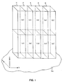
- a unit cell crystal structure compatible with superconductivity is shown in Figure 1 oriented on a monocrystalline substrate surface Ss .
- the longest dimension of the unit cell, its c-axis, is oriented normal to the substrate surface parallel to arrow c .
- the two remaining orthogonal (mutually perpendicular) axes of the unit cell are parallel to the substrate surface and parallel to the arrows a and b .
- Five unit cell sub-units 1 , 2 , 3 , 4 and 5 are shown on the substrate surface, each sub-unit including (a) and (b) portions relatively displaced along the c-axis (the axis of longest length).
- the unit cell a-axis (the axis of shortest length) is one sub-unit in length. Notice that the unit cell faces parallel to the c-axis (that is, the vertical unit cell faces as shown in Figure 1) are also each oriented parallel to one of the a and b-axes.
- the oxides of formula I can form any one of three different superconductive crystal structures, depending upon the value of n .
- n is 2, 1 or zero
- the black spheres represent copper
- the unlabeled spheres represent oxygen
- the spheres labeled B , C and B represent bismuth, calcium and strontium, respectively.
- an entire atom is shown in each occurrence where any portion of the atom is included in a sub-unit.
- each (a) sub-unit form the four corner tiers of each (b) sub-unit and vice versa .
- the sole difference between an increment of layer thickness formed by (a) sub-units and an increment of layer thickness formed by (b) sub-units is a relative shift of one half sub-unit along each of the a and b-axes.
- the c-axes of the unit cells of the crystalline oxide are oriented normal to the substrate surface, as shown in Figure 1.
- the minor axes (the a and b-axes) are parallel to the substrate surface, with the a and b-axes of each unit cell being orthogonally related. Over the entire surface of the thin film there is, however, a wide array of different angular orientations of minor axes.
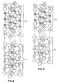
- the conventional angular deviation from alignment of the minor axes of unit cells in a conventional crystalline oxide thin film is shown in Figure 5.
- the joined arrow pairs each indicate the minor axes orientations viewed normal to the substrate surface in that area of the film. While the arrows in each joined pair exhibit a 90° angle of intersection, significant angular displacements of minor axes orientations are observed in different film areas.
- microcrystalline film segments (hereinafter referred to as grains or microcrystals) separated by high angle intergrain boundaries.
- a grain boundary (not shown in Figure 5) separates each minor axes pair from each next adjacent non-aligned minor axes pair.
- Individual microcrystalline grains on average typically have a projected area viewed normal to the substrate surface of less than about 100 ⁇ m2. The areas of the individual grains correlate inversely with the number of high angle intergrain boundaries. Thus, the smaller the mean projected areas of the grains, the greater the number of high angle grain boundaries and the more internal disruptions to superconduction within the thin films. Thus, conventional thin films suffer the disadvantage of exhibiting significantly limited superconductive current carrying capacity.
- a superconductive crystalline oxide layer is epitaxially grown on a monocrystalline substrate surface with a high degree of matching not only of c-axis orientations, but also of minor axes orientations. In every instance at least 50 percent (preferably greater than 70 percent and optimally greater than 90 percent) of the unit cells forming the superconductive layers are oriented with their c-axes normal to the substrate surface and with their minor axes relatively angularly aligned within a deviation range of less than 5°.
- the feature of c-axis orientation normal to the substrate surface can be realized for substantially all of the unit cells in a thin film, with overall deviations of less than 2° (often less than 1°) from normal of the c-axes being observed.
- the distribution of the c-axes are determined by rocking curve analysis.
- the orientation of the crystal minor axes of the unit cells are determined by the X-ray pole figure analysis technique. These techniques are well understood by those skilled in the art and are illustrated by B. D. Cullity, Elements of X-ray Diffraction , 2nd Ed., Addison-Wesley, Reading, Ma., Chapters 8 and 9, the disclosure of which is here incorporated by reference.
- a point source of X-radiation is reflected from the surface of the thin film with the thin film oriented with a selected set of parallel crystallographic planes within the thin film oriented parallel to the reflection-surface. The thin film is then rotated about an axis normal to the selected cristal planes.
- Reflection over a wide range of rotation angles indicates a wide range of unit cell axis orientations, while ideal alignment is seen as four spot reflections separated one from the other by a 90° rotation angle. In practice even in the closest alignments produce spots that subtend at least a small azimuth angle of rotation.
- a crystalline oxide thin film satisfying the composition of formula I is shown with minor axes pairs each representing minor axes orientations in different areas of the film.
- the c-axes are all normal to the underlying (not shown) substrate surface, but, unlike Figure 5, the minor axes pairs are largely in angular alignment from one area of the film to the next.
- near point that is, narrow azimuth angle
- reflections are observed subtending an azimuth angle of much less than 5°, with actual observations being of point deviations of less than 4°, typically in the order of 2°. This is indicative of a sharply diminished area to area angular deviation of the minor axes pairs shown in Figure 6.
- the invention allows thin films, those of less than 5 ⁇ m thickness (most commonly less than 2 ⁇ m in thickness and optimally less than 1 ⁇ m in thickness) to be realized that exhibit both high superconductive current densities and high temperatures of superconductivity.
- Superconducting onset (T o ) temperatures in excess of the temperature of liquid nitrogen (77°K) can be realized with the compositions of formula I, and superconducting transition tmeperatures (T c ) of greater than 100°K are contemplated.
- Maximum superconducting temperatures are realized when n in formula I is 2, with progressively lower temperatures being realizable when n is 1 or zero. When n is zero both T o and T c are well below the 77°K and 100°K values noted above.
- the orientation of the thin film crystalline oxide is derived from the crystalline order of the monocrystalline substrate surface.
- Substrate surfaces that exhibit a perovskite crystal structure are particularly compatible with supporting formation of the oriented crystalline oxide thin film.
- Exemplary of preferred perovskites for forming the substrate surface are strontium titanate, lanthanum aluminate, lanthanum gallium oxide and potassium tantalate.
- monocrystalline magnesium oxide magnesia
- hafnium oxide hafnia
- zirconium oxide zirconia
- Hafnium and zirconium have almost identical chemical and physical properties and can be used interchangeably or mixed in any proportions. As between hafnia and zirconia the latter is less expensive and therefore much more extensively employed in the art.
- Yttria stabilized zirconia where yttrium displaces from 5 to 15 percent of the zirconium on an atomic basis, is a monocrystalline substrate that has been widely used in fabricating superconductive films.
- the crystal surface presented by the substrate for deposition of the oriented crystalline oxide thin film is preferably a ⁇ 100 ⁇ surface.
- the substrates can take any convenient form capable of providing the required monocrystalline surface.
- the substrate can, for example, be a unitary element formed throughout by a single monocrystalline material.
- the substrate can contain a monocrystalline support structure onto which one or more layers are epitaxially grown to form the required monocrystalline substrate surface.
- monocrystalline layers of monocrystalline layers of strontium titanate have been epitaxially grown, as disclosed by H. Ishiwara and K. Azuma, "Oriented Growth of SrTiO3 Films on Si(100) Substrates Using In-Situ Cleaning by Excited Hydrogen", Mat. Res. Soc. Symp. Proc., Vol. 116, 1988 Materials Research Society, pp.
- Bi4Ti3O12 CaBi4Ti4O15; SrBi4Ti4O15; BaBi4Ti4O15; PbBi4Ti4O15; Sr2Bi4Ti5O18; Ba2Bi4Ti5O18; and Pb2Bi4Ti5O18.
- the metals to be incorporated in the film are each employed as starting materials in the form of metal-ligand compounds, where each metal-ligand compound includes at least one thermally volatilizable organic ligand.
- the organic ligands are selected for their film forming capabilities. In general the film forming capabilities of the organic ligands increase as a function of the number of carbon atoms they contain and as a function of chain branching, cyclic hydrocarbons and branched hydrocarbon chains being capable of producing superior films with fewer carbon atoms than linear hydrocarbon chains. Typically organic ligands are selected that contain up to about 30 carbon atoms.
- Individual metal ligands can have as few as 2 carbon atoms (that is, individual metal acetates are feasible), but preferably contain from 6 to 20 carbon atoms.
- hydrocarbons or substituted hydrocarbons preferably branched chain hydrocarbons or substituted hydrocarbons such as terpenes, of from 10 to 30 carbon atoms can be incorporated to assist in film formation.
- metal-ligand compounds are selected on their ability to thermally decompose rather than vaporize.
- Metal-organic ligand compounds including metallo-organic and organo-metallic compounds, such as metal alkyls, alkoxides, ⁇ -diketone derivatives and metal salts of organic acids--for example, carboxylic acids, constitute preferred metal-ligand compounds. Copper is preferably employed as a metal carboxylate to minimize copper loss by vaporization.
- Exemplary preferred organic ligands for the metal organic compounds include metal butyrates, 2-ethylhexanoates, naphthenates, neodecanoates, butoxides, isopropoxides, rosinates (for example, abietates), cyclohexanebutyrates and acetylacetonates.
- Exemplary film-forming agents include 2-ethylhexanoic acid, rosin (for example, abietic acid), ethyl lactate, 2-ethyoxyethyl acetate and pinene.
- any convenient thermally decomposable or volatilizable solvent for the metal-ligand compounds and the film-forming agents can be employed.
- Exemplary preferred film forming solvents include toluene, 2-ethylhexanoic acid, n-butyl acetate, ethyl lactate, propanol, pinene and mineral spirits.
- the requisite fluorine content can be incorporated in the metal-organic ligand coatings by introducing any convenient organic compound having one or more fluorine to carbon bonds. While fluoro-substituted organic compounds can be selected solely for their utility in supplying the required fluorine atoms, it is preferred to select fluoro-substituted organic compounds satisfying the film forming characteristics discussed above to insure intimate dispersion of the fluorine atoms in the coatings. In a specifically preferred form of the invention the ligands of the metal-organic compounds and/or the film-forming agents are fluoro-substituted, thereby obviating the necessity of including yet another ingredient in forming the coating.
- the coating composition is applied to the monocrystalline support surface by any convenient coating technique.
- Spin casting is a particularly preferred technique, since it allows control of both the thickness and uniformity of the spin cast layer.
- Spin casting is well suited for laying down layers of up to about 1.5 ⁇ m in thickness, but spin cast layers are typically less than 1.0 ⁇ m in thickness.
- the coated substrate is heated to a temperature sufficient to volatilize or decompose thermally the organic components of the coating. While removal temperatures vary as a function of the organic components selected, no organic residue remains at a temperature of 600°C. Although this temperature is well in excess of that required to remove organic residues from the coating, it is still well below the temperatures required for crystalline oxide formation.
- the coating after heating is much thinner than that originally coated. If a thicker crystalline oxide coating is desired than can be generated using a single spin casting step, it is recognized that the spin casting step and the heating step can be repeated, once or several times, in sequence to achieve the desired crystalline oxide film thickness. Successive coating and heating steps also offer the advantage of better protecting the coating from substrate contaminants, if present.
- Conversion of the coating after removal of organic residues to a crystalline oxide with unit cell axial alignment can be achieved at temperatures in the range of from 800 to 860°C.
- Crystallization temperatures are a function of both the lead content of the coating and the crystalline form being formed.
- the 2101, 2212 and 2223 crystalline forms require progressively high temperatures for their formation.
- preferred firing temperatures are in the range of from 800 to 840°C.
- preferred firing temperatures are in the range of from 800 to 850°C, which is below the 850 to 920°C preferred range for the 2212 crystalline form taught by Agostinelli and others.
- For the 2223 crystalline form preferred firing temperatures are in the range of from 800 to 860°C, which is well below the approximately 890°C firing temperature typically employed to produce this crystalline form.
- the steps of coating, heating and firing described above can be repeated in sequence two or more times to produce a thin film having increased mean grain projected areas.
- crystalline oxides with unit cell aligned crystal axes can take any convenient conventional form.
- the thin films can, for example, be formed as taught by Agostinelli, cited above, except as otherwise noted.
- a metal-organic ligand composition containing bismuth, strontium, calcium and copper in a 2:2:1:2 atomic ratio (hereinafter referred to as 2212 Precursor 1) was prepared by mixing a bismuth precursor composition containing bismuth 2-ethylhexanoate, a strontium precursor composition containing strontium cyclohexanebutyrate, a calcium precursor composition containing calcium 2-ethylhexanoate and a copper precursor composition containing copper 2-ethylhexanoate.
- the bismuth precursor, containing 18.73% by weight bismuth, and the calcium precursor, containing 4.10% by weight calcium were prepared as described by Agostinelli and others U.S. Patent 4,950,643.
- the strontium precursor was strontium cyclohexane-butyrate purchased commercially with an assay indicating a strontium concentration of 19.4% by weight strontium.
- the copper precursor with a copper concentration of 6.31% by weight, was prepared by mixing 2.0 g of copper acetate with 8.0 g of 2-ethyl-hexanoic acid. The individual precursors were mixed in a weight ratio of 1:0.438:0.405:0.903 and then heated to boiling until no solids remained.
- the 2212 Precursor 1 had a concentration of about 1.63 X 10 ⁇ 4 mole (based on the 2212 crystalline oxide to be formed) per gram.
- Kodak 2315TM rosin
- Precursor 1 was spin coated on a ⁇ 100 ⁇ crystal surface of magnesium oxide at 4000 rpm for 20 seconds. The coated film was then heated on a hot plate to a thermal decomposition temperature of 450°C. The coating then fired in air at a temperature of 865°C for 10 minutes in air.
- Microscopic examination revealed a polycrystalline coating on the substrate surface having a mean grain effective circular diameter (ECD) in the range of from 1 to 2 ⁇ m.
- ECD mean grain effective circular diameter
- X-ray diffraction analysis of c-axis alignment revealed a large number of c-axis misaligned grains.
- the superconducting onset temperature T o was determined to be 76°K.
- the critical current density increased slowly with decreasing temperature, reaching a value of approximately 1 X 10⁴ A/cm2 at 40°K.
- the magnetic susceptibility measured versus temperature exhibited a strong field dependence, corroborating poor intergranular conductivity and low critical current.
- This control demonstrates low critical currents produced by a conventional procedure of preparing a superconductive 2212 bismuth strontium calcium copper oxide crystalline oxide coating with a high level of c-axis misalignment on a monocrystalline magnesia substrate surface.
- Example 2 repeated the steps of Example 1, except that the final film was built up using four repetitions of the coating, heating and firing steps, with each repetition producing a layer having a thickness of 60 nm, measured after hot plate heating.
- the four-layer coating had an overall thickness of 250 nm.
- Rocking curve analysis revealed a high degree of c-axis orientation normal to the substrate surface, with 50 percent of the microcrystals having c-axis orientations deviating from the perpendicular by less than 0.3° to 0.4°.
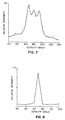
- X-ray diffraction analysis of minor axis orientations revealed a high degree of angular misalignment. This is demonstrated in Figure 7 by the three diffraction peaks covering a range of about 40° with an angle of 12 to 13° separating adjacent peaks.
- the superconducting onset temperature was 80°C, and the critical current remained low with magnetic susceptibility still showing a strong field dependence.
- Example 1 The procedure of Example 1 was repeated, except that (a) the 2212 Precursor 1 was mixed with heptafluorobutyric acid at a ratio of 1:0.17 (F:Sr atomic ratio 8:1) and firing was conducted for 30 minutes at 820°C. Some grains were 30 to 50 ⁇ m wide and several hundred ⁇ m long.
- the superconducting onset temperature T o was determined to be 81°K.
- the critical current density increased slowly with decreasing temperature, reaching a value of approximately 9 X 10⁴ A/cm2 at 40°K.
- the magnetic susceptibility measured versus temperature exhibited a much weaker field dependence than in Example 1.
- Example 1 was repeated, except that coating was undertaken onto the ⁇ 100 ⁇ monocrystalline surface of a strontium titanate perovskite.
- the thin film produced was essentially similar to that of Example 1 in its crystal structure and conduction properties.
- Example 4 The procedure of Example 4 was repeated, except that (a) the 2212 Precursor 1 was mixed with heptafluorobutyric acid at a ratio of 1:0.17 (F:Sr atomic ratio 8:1) and firing was conducted for 30 minutes at 820°C.
- X-ray diffraction, optical microscopy and Raman spectrometry measurements revealed c-axis normal alignment on the substrate surface with the minor axes also being angularly aligned.
- the alignment of the microcrystals on the surface of the substrate is shown in Figure 9(b).
- X-ray pole figure examination showed a narrow spot pattern, corroborative of angular alignment of the minor axes of the crystal unit cells.
- This example demonstrates the effectiveness of a fluoro-substituted organic compound when incorporated in the initial coating to increase axial alignment of the crystalline oxide and hence the superconductive current carrying capacity of the thin films.
- This example further demonstrates the utility of a substrate surface exhibiting a perovskite crystal structure in realizing the advantages of the invention.
- Example 5 was repeated, except that the F:Sr atomic ratio in the coating was reduced to 4:1 by decreasing the amount of heptafluorobutyric acid introduced into the initial coating composition.
- the thin film crystal and conduction properties were similar to those of Example 5.
- Example 5 was repeated, except that the F:Sr atomic ratio in the coating was reduced to 2:1 by decreasing the amount of heptafluorobutyric acid introduced into the initial coating composition.
- the thin film produced was granular in appearance, similar to the thin film of Example 1, but with the mean ECD of the grains increased to 5 to 6 ⁇ m.
Landscapes
- Engineering & Computer Science (AREA)
- Chemical & Material Sciences (AREA)
- Manufacturing & Machinery (AREA)
- Ceramic Engineering (AREA)
- Crystallography & Structural Chemistry (AREA)
- Superconductors And Manufacturing Methods Therefor (AREA)
- Crystals, And After-Treatments Of Crystals (AREA)
- Superconductor Devices And Manufacturing Methods Thereof (AREA)
- Inorganic Compounds Of Heavy Metals (AREA)
Applications Claiming Priority (2)
| Application Number | Priority Date | Filing Date | Title |
|---|---|---|---|
| US75597491A | 1991-09-06 | 1991-09-06 | |
| US755974 | 1991-09-06 |
Publications (2)
| Publication Number | Publication Date |
|---|---|
| EP0531236A2 true EP0531236A2 (de) | 1993-03-10 |
| EP0531236A3 EP0531236A3 (de) | 1993-05-12 |
Family
ID=25041478
Family Applications (1)
| Application Number | Title | Priority Date | Filing Date |
|---|---|---|---|
| EP19920420287 Withdrawn EP0531236A3 (de) | 1991-09-06 | 1992-08-31 | Verbesserte supraleitende Schicht auf monokristallinem Substrat und Verfahren zu ihrer Herstellung |
Country Status (3)
| Country | Link |
|---|---|
| EP (1) | EP0531236A3 (de) |
| JP (1) | JPH05238894A (de) |
| CA (1) | CA2076279A1 (de) |
Cited By (1)
| Publication number | Priority date | Publication date | Assignee | Title |
|---|---|---|---|---|
| EP1022255A4 (de) * | 1997-01-29 | 2006-09-06 | Mikio Takano | Oxid-supraleiter |
Families Citing this family (15)
| Publication number | Priority date | Publication date | Assignee | Title |
|---|---|---|---|---|
| US6392257B1 (en) | 2000-02-10 | 2002-05-21 | Motorola Inc. | Semiconductor structure, semiconductor device, communicating device, integrated circuit, and process for fabricating the same |
| KR20030011083A (ko) | 2000-05-31 | 2003-02-06 | 모토로라 인코포레이티드 | 반도체 디바이스 및 이를 제조하기 위한 방법 |
| AU2001277001A1 (en) | 2000-07-24 | 2002-02-05 | Motorola, Inc. | Heterojunction tunneling diodes and process for fabricating same |
| US20020096683A1 (en) | 2001-01-19 | 2002-07-25 | Motorola, Inc. | Structure and method for fabricating GaN devices utilizing the formation of a compliant substrate |
| WO2002082551A1 (en) | 2001-04-02 | 2002-10-17 | Motorola, Inc. | A semiconductor structure exhibiting reduced leakage current |
| US6992321B2 (en) | 2001-07-13 | 2006-01-31 | Motorola, Inc. | Structure and method for fabricating semiconductor structures and devices utilizing piezoelectric materials |
| US7019332B2 (en) | 2001-07-20 | 2006-03-28 | Freescale Semiconductor, Inc. | Fabrication of a wavelength locker within a semiconductor structure |
| US6855992B2 (en) | 2001-07-24 | 2005-02-15 | Motorola Inc. | Structure and method for fabricating configurable transistor devices utilizing the formation of a compliant substrate for materials used to form the same |
| US20030034491A1 (en) | 2001-08-14 | 2003-02-20 | Motorola, Inc. | Structure and method for fabricating semiconductor structures and devices for detecting an object |
| US20030071327A1 (en) | 2001-10-17 | 2003-04-17 | Motorola, Inc. | Method and apparatus utilizing monocrystalline insulator |
| US6916717B2 (en) | 2002-05-03 | 2005-07-12 | Motorola, Inc. | Method for growing a monocrystalline oxide layer and for fabricating a semiconductor device on a monocrystalline substrate |
| US7169619B2 (en) | 2002-11-19 | 2007-01-30 | Freescale Semiconductor, Inc. | Method for fabricating semiconductor structures on vicinal substrates using a low temperature, low pressure, alkaline earth metal-rich process |
| US6885065B2 (en) | 2002-11-20 | 2005-04-26 | Freescale Semiconductor, Inc. | Ferromagnetic semiconductor structure and method for forming the same |
| US7020374B2 (en) | 2003-02-03 | 2006-03-28 | Freescale Semiconductor, Inc. | Optical waveguide structure and method for fabricating the same |
| US6965128B2 (en) | 2003-02-03 | 2005-11-15 | Freescale Semiconductor, Inc. | Structure and method for fabricating semiconductor microresonator devices |
Family Cites Families (2)
| Publication number | Priority date | Publication date | Assignee | Title |
|---|---|---|---|---|
| CA2015018A1 (en) * | 1989-05-04 | 1990-11-04 | Mark Lelental | Processes of forming conductive films and articles so produced |
| US5086035A (en) * | 1990-02-06 | 1992-02-04 | Eastman Kodak Company | Electrically conductive article (i) |
-
1992
- 1992-08-17 CA CA002076279A patent/CA2076279A1/en not_active Abandoned
- 1992-08-31 EP EP19920420287 patent/EP0531236A3/de not_active Withdrawn
- 1992-09-07 JP JP4262719A patent/JPH05238894A/ja active Pending
Cited By (1)
| Publication number | Priority date | Publication date | Assignee | Title |
|---|---|---|---|---|
| EP1022255A4 (de) * | 1997-01-29 | 2006-09-06 | Mikio Takano | Oxid-supraleiter |
Also Published As
| Publication number | Publication date |
|---|---|
| EP0531236A3 (de) | 1993-05-12 |
| CA2076279A1 (en) | 1993-03-07 |
| JPH05238894A (ja) | 1993-09-17 |
Similar Documents
| Publication | Publication Date | Title |
|---|---|---|
| EP0531236A2 (de) | Verbesserte supraleitende Schicht auf monokristallinem Substrat und Verfahren zu ihrer Herstellung | |
| US6562761B1 (en) | Coated conductor thick film precursor | |
| EP0406126B1 (de) | Substrat mit einer supraleitenden Schicht | |
| US5032568A (en) | Deposition of superconducting thick films by spray inductively coupled plasma method | |
| EP0461050B1 (de) | Zusammensetzungen von kubischer Perowskit-Kristallstruktur, Verfahren zu ihrer Herstellung und Produkte daraus | |
| Fork et al. | Effects of homoepitaxial surfaces and interface compounds on the in-plane epitaxy of YBCO films on yttria-stabilized zirconia | |
| US8389045B2 (en) | Method for producing oxide superconductor | |
| US20040121191A1 (en) | Buffer layers and articles for electronic devices | |
| JPH01320224A (ja) | 超伝導体構造体 | |
| US7919434B2 (en) | Oxide superconducting film and method of preparing the same | |
| Mercey et al. | Thin film deposition: a novel synthetic route to new materials | |
| JPH05508610A (ja) | a,b軸方向のペロブスカイト薄膜の成長方法 | |
| Dawley et al. | Thick Sol-gel Derived YBaCuO, 5 Films | |
| JP2007307904A (ja) | 被覆された伝導体及び高温超伝導体層の製造に有用な多結晶質フィルム | |
| US4950643A (en) | Metalorganic deposition process for preparing heavy pnictide superconducting oxide films | |
| Qi et al. | Liquid-phase epitaxial growth of REBa2Cu3O7− δ (RE= Y, Yb, Er) thick films at reduced temperatures | |
| Shi et al. | The development of Y Ba2Cu3O x thin films using a fluorine-free sol–gel approach for coated conductors | |
| EP0624663B1 (de) | Verbundmaterial und Verfahren zu seiner Herstellung | |
| US5082688A (en) | Processes of forming Ag doped conductive crystalline bismuth mixed alkaline earth copper oxide films | |
| KR930008648B1 (ko) | 페로브스키트형 초전도체막 준비공정 | |
| Hughes et al. | In situ growth of PbSrYCaCuO films by laser ablation | |
| US5145832A (en) | Superconducting film on a flexible two-layer zirconia substrate | |
| EP0531237A2 (de) | Supraleitende Dünnschichten mit verstärkten Korngrösse und Verfahren zu ihrer Herstellung | |
| US5118662A (en) | Article comprising conductive film of crystalline bismuth mixed alkaline earth oxide containing silver | |
| US5041417A (en) | Conductive articles and intermediates containing heavy pnictide mixed alkaline earth oxide layers |
Legal Events
| Date | Code | Title | Description |
|---|---|---|---|
| PUAI | Public reference made under article 153(3) epc to a published international application that has entered the european phase |
Free format text: ORIGINAL CODE: 0009012 |
|
| AK | Designated contracting states |
Kind code of ref document: A2 Designated state(s): AT BE CH DE DK ES FR GB GR IE IT LI LU MC NL PT SE |
|
| PUAL | Search report despatched |
Free format text: ORIGINAL CODE: 0009013 |
|
| AK | Designated contracting states |
Kind code of ref document: A3 Designated state(s): AT BE CH DE DK ES FR GB GR IE IT LI LU MC NL PT SE |
|
| 18D | Application deemed to be withdrawn |
Effective date: 19931113 |