EP0532175B1 - Dispositif optique utilisant l'effet de superresolution - Google Patents
Dispositif optique utilisant l'effet de superresolution Download PDFInfo
- Publication number
- EP0532175B1 EP0532175B1 EP92307274A EP92307274A EP0532175B1 EP 0532175 B1 EP0532175 B1 EP 0532175B1 EP 92307274 A EP92307274 A EP 92307274A EP 92307274 A EP92307274 A EP 92307274A EP 0532175 B1 EP0532175 B1 EP 0532175B1
- Authority
- EP
- European Patent Office
- Prior art keywords
- optical
- light
- lens
- light beam
- objective lens
- Prior art date
- Legal status (The legal status is an assumption and is not a legal conclusion. Google has not performed a legal analysis and makes no representation as to the accuracy of the status listed.)
- Expired - Lifetime
Links
- 230000003287 optical effect Effects 0.000 title claims description 94
- 230000000694 effects Effects 0.000 title description 3
- 239000000758 substrate Substances 0.000 claims description 31
- 230000002093 peripheral effect Effects 0.000 claims description 3
- 239000004065 semiconductor Substances 0.000 description 11
- XAGFODPZIPBFFR-UHFFFAOYSA-N aluminium Chemical compound [Al] XAGFODPZIPBFFR-UHFFFAOYSA-N 0.000 description 3
- 229910052782 aluminium Inorganic materials 0.000 description 3
- 239000011521 glass Substances 0.000 description 3
- 238000000034 method Methods 0.000 description 3
- 238000000151 deposition Methods 0.000 description 2
- 238000001514 detection method Methods 0.000 description 2
- 238000004519 manufacturing process Methods 0.000 description 2
- XUIMIQQOPSSXEZ-UHFFFAOYSA-N Silicon Chemical compound [Si] XUIMIQQOPSSXEZ-UHFFFAOYSA-N 0.000 description 1
- 230000004075 alteration Effects 0.000 description 1
- 201000009310 astigmatism Diseases 0.000 description 1
- 230000000903 blocking effect Effects 0.000 description 1
- 238000003486 chemical etching Methods 0.000 description 1
- 239000013078 crystal Substances 0.000 description 1
- 238000006073 displacement reaction Methods 0.000 description 1
- 238000009826 distribution Methods 0.000 description 1
- 230000010354 integration Effects 0.000 description 1
- 238000012986 modification Methods 0.000 description 1
- 230000004048 modification Effects 0.000 description 1
- 230000000644 propagated effect Effects 0.000 description 1
- 230000035939 shock Effects 0.000 description 1
- 229910052710 silicon Inorganic materials 0.000 description 1
- 239000010703 silicon Substances 0.000 description 1
Images


Classifications
-
- G—PHYSICS
- G11—INFORMATION STORAGE
- G11B—INFORMATION STORAGE BASED ON RELATIVE MOVEMENT BETWEEN RECORD CARRIER AND TRANSDUCER
- G11B7/00—Recording or reproducing by optical means, e.g. recording using a thermal beam of optical radiation by modifying optical properties or the physical structure, reproducing using an optical beam at lower power by sensing optical properties; Record carriers therefor
- G11B7/12—Heads, e.g. forming of the optical beam spot or modulation of the optical beam
- G11B7/135—Means for guiding the beam from the source to the record carrier or from the record carrier to the detector
- G11B7/1372—Lenses
- G11B7/1374—Objective lenses
-
- G—PHYSICS
- G02—OPTICS
- G02B—OPTICAL ELEMENTS, SYSTEMS OR APPARATUS
- G02B27/00—Optical systems or apparatus not provided for by any of the groups G02B1/00 - G02B26/00, G02B30/00
- G02B27/58—Optics for apodization or superresolution; Optical synthetic aperture systems
-
- G—PHYSICS
- G11—INFORMATION STORAGE
- G11B—INFORMATION STORAGE BASED ON RELATIVE MOVEMENT BETWEEN RECORD CARRIER AND TRANSDUCER
- G11B7/00—Recording or reproducing by optical means, e.g. recording using a thermal beam of optical radiation by modifying optical properties or the physical structure, reproducing using an optical beam at lower power by sensing optical properties; Record carriers therefor
- G11B7/12—Heads, e.g. forming of the optical beam spot or modulation of the optical beam
- G11B7/123—Integrated head arrangements, e.g. with source and detectors mounted on the same substrate
-
- G—PHYSICS
- G11—INFORMATION STORAGE
- G11B—INFORMATION STORAGE BASED ON RELATIVE MOVEMENT BETWEEN RECORD CARRIER AND TRANSDUCER
- G11B7/00—Recording or reproducing by optical means, e.g. recording using a thermal beam of optical radiation by modifying optical properties or the physical structure, reproducing using an optical beam at lower power by sensing optical properties; Record carriers therefor
- G11B7/12—Heads, e.g. forming of the optical beam spot or modulation of the optical beam
- G11B7/135—Means for guiding the beam from the source to the record carrier or from the record carrier to the detector
- G11B7/1381—Non-lens elements for altering the properties of the beam, e.g. knife edges, slits, filters or stops
Definitions
- the present invention relates to an optical device of a small size. More particularly, the present invention relates to an optical device miniaturized by allowing light to operate in a confined small space. Such optical devices are particularly suitable for optical pick-up devices, laser printers, and sensors, which require little space and light weight. In general, the optical device has two types; an integrated type and a substrate type.
- optical information processors In recent years, various kinds of optical information processors have been developed. Typical examples are compact disks that are widely used instead of gramophone records, electronic filing systems for storing documents and photographs in magneto-optical disks, and laser printers for writing information in a recording section of a copying machine with a laser beam.
- An optical information processor is also used in automated manufacturing equipment as an optical encoder and an optical range finder.
- a compact disk system is provided with pits having a depth of about 1/2 wave depth which are intended to indicate digital signals "1" and "0". By reading data in terms of the pits the data is reproduced on a phonograph record.
- the pit data is optically read so that large spaces are not required for one bit data but only a tiny area of about 1 ⁇ m 2 is sufficient. This leads to a highly dense recording system. Because of this advantage, compact disks are becoming more popular than magnetic tapes or magnetic disks.
- the compact disk requires an optical component such as a pick-up device for reading pit data.
- the optical components include a lens, a beam splitter and other components, and the assemblage and adjustment of these are time- and labor-consuming.
- the size is likely to become large and heavy, and the cost is likely to be high.
- FIG. 3 shows a known optical pick-up device intended to overcome the problems mentioned above.
- This optical device is a self-contained system 59 which includes a hologram 55 formed on a glass plate 52 so as to enable it to function as a beam splitter and a diffracting grating, a semiconductor laser 51 as an optical source and an optical detector 56 for detecting signals.
- the pick-up device is operated as follows:
- a laser beam D emitted upward from the semiconductor laser 51 is focused on an optical disk 57 through a collimator lens 53 and a focusing lens 54 both disposed above the hologram 55.
- the light reflecting upon the disk 57 reversely follows the above-mentioned path but is deflected by the hologram 55, the light being detected by the detector 56.
- the focusing lens 54 is adjusted as to its position and focal point by means of an actuator (not shown) using an electromagnet.
- This known pick-up device is comparatively lightweight because of a reduced number of components as well as a reduced size of each component, but ideally, the desired weight should be much lighter.
- the components it is only the focusing lens 54 that can be moved by the actuator because of its light weight.
- Figure 4 shows another pick-up device designed to solve the problems pointed out above.
- a typical example of this device is disclosed in Japanese Laid-Open Patent Publication No. 62-117150.
- a three beam generating grating 62, a collimator diffracting grating 63, astigmatism generating lenses 76 and 77, a semiconductor laser 71 and an optical detector 78 are all mounted on a glass plate, except for a focusing lens 75 for focusing a source light on the disk 57.
- a substrate type pick-up device can be smaller in size than an ordinary pick-up device because the source light is propagated through the substrate 61 even though the distance between the light source and optical disk 57 is the same.
- the small pick-up device requires the laser beam to be as small as possible in diameter so as to pass through the focusing lens without divergence.
- the advantage of the small size is traded off against the necessity for requiring a highly precision focusing lens 75.
- the focusing lens 75 is not mounted on the substrate 61 which prevents the size of the pick-up device from being reduced beyond a certain limit.
- the beam In order to make most use of the characteristics of light, the beam must be sufficiently focused on the optical disk 57.
- the numerical aperture NA is nearly equal to d/2f where d is the smaller of the diameter of the lens or the diameter of the laser beam (i.e. the effective diameter of the lens), and f is the focal length of the lens.
- the minimum diameter 2W 0 of the beam is called "diffraction limit".
- a lens has a larger numerical aperture NA, the beam can be focused smaller but this results in more abberation and difficulty in fabrication. If the device is to be made compact, the diameter of the beam must be reduced, but in order to maintain the numerical aperture NA constant, the focal length must be reduced. This requires the lens face to have a small curvature, but it is likely to cause aberration. Since a substrate type pick-up device has a relatively short distance from the light source to the focusing lens 75, the effective diameter of the focusing lens 75 can be relatively small. As a result, it is difficult to produce focusing lenses having a large numerical aperture NA.
- Any other optical systems such as hologram laser printers cannot be miniaturized without sacrificing the focusability of the lens.
- the reduction in the focusability restricts the range of application.
- a super-resolution lens is disposed separately from the optical pick-up system. This necessitates the movement of the lens in accordance with that of the pits in the optical disk 57. Because of this movement, the light beam is likely to deviate from the central portion of the lens, thereby failing to achieve the desired focusing characteristics.
- an optical pick-up device for reading an optical disc, the device comprising: an optical system of optical components, the optical system comprising a light source, a reflective element, an objective lens, a beam splitter and an optical detector, wherein the lens, the beam splitter and the optical detector are disposed, in use, in a path of light from the light source; and wherein the optical system is configured so that a light beam is prevented from focusing through a central portion of the lens, whereby the lens focuses light to below the diffraction limit.
- the lens is not mounted on a substrate, so it is not possible to minaturise the optical device, for the reasons given above. Furthermore, a high precision lens is required, again as described above.
- an optical system of the above type characterised in that the light source, the beam splitter and the optical detector are disposed on a light transmissive substrate ; and in that the objective lens has an aspheric face and is integral with the light transmissive substrate for receiving the light from the light source which passes through the light transmissive substrate.
- the objective lens comprises a central portion which differentiates the optical characteristics of a light beam incident on the central portion from the properties of a light beam incident on a peripheral portion thereof.
- the optical system is configured so that a light beam is prevented from passing through a central portion of the objective lens.
- a central portion of said objective lens is flattened to negate focusibility thereof.
- a central portion of said objective lens prevents a light beam from passing therethrough.
- the light beam from the light source passes the objective lens so as to irradiate an optical disc on the outside of the optical system with the light beam.
- the light beam from the outside of the optical system passes the objective lens so as to make the light beam incident upon another one of the optical components in the optical system.
- the invention described herein makes possible the advantages of (1) providing an optical device miniaturized without sacrificing optical characteristics, and (2) providing an optical device allowing the integration of optical components in a relatively small space.
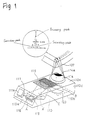
- the exemplary embodiment is a substrate type optical pick-up device which has a multi-sided substrate 110 of transparent glass.
- the substrate 110 includes an optical system including optical components.
- the substrate 110 has an inclined face 110a at one end on which a semiconductor laser 111 is disposed as a light source to which a submount 111a made of a silicon substrate having an intergrated semiconductor laser driving circuit (not shown) is connected.
- the semiconductor laser 111 and submount 111a are integrated with the inclined face 110a .
- a light beam A from the semiconductor laser 111 enters the substrate 110 , and is injected into a diffracting grating 119.
- the light beam A is split into three beams A' having different angles of reflection ⁇ .
- the three beams A' are injected into a diffracting grating 115 formed on the top surface 110c of the substrate 110 , the diffraction grating 115 including two kinds of hologram beam splitters having different grating period.
- the diffraction grating 115 splits the light beams A' into a light beam reflected thereon and diffracted light beams which are not used in Example 1.
- the light beams reflected on the diffraction grating 115 are diffracted vertically upwards by a diffraction grating 123 formed on the bottom 110b and converted into parallel light beams B .
- the parallel beams B are focused by a super-resolution lens 114 integral with a portion of the substrate 110 corresponding to the diffraction grating 123 whereby they are focused on an optical disk 107 .
- the super-resolution lens 114 is formed by depositing an aluminum film 114a around the center of an aspheric lens.
- it is preferable that the aluminum depositing portion 114a is roughened by a chemical etching so as to prevent the reflecting light beam from returning to the semiconductor laser 111 .
- Circled in Figure 1 is an enlarged view which shows the distribution of optical intensity possessed by each spot on the optical disk 107, and according to the super-resolution lens 114, the diameter 2W 0 of the beam can be reduced by 70% than when an ordinary lens is used.
- each optical spot includes two secondary peaks which appear on each side of a primary peak.
- the light beam reflecting upon the optical disk 107 passed through the super-resolution lens 114 and is converted into parallel light beams. Then, they are split into a diffracted light beam C and a reflecting light beam by the diffracting grating 115 . In the illustrated example, this reflecting light is not used.
- the diffracted light beam C is injected into a sextant detector 116 formed on the inclined face 110a of the substrate 110 which is formed adjacent to the semiconductor laser 111 so as to detect signals, a focal point, and the positions of pits.
- a sextant detector 116 formed on the inclined face 110a of the substrate 110 which is formed adjacent to the semiconductor laser 111 so as to detect signals, a focal point, and the positions of pits.
- Part of the secondary-peaked reflecting light beams results in noise but the noise is not so strong as a signal which would be caused by the primary peak, thereby providing no problem in detection.
- the super-resolution lens 114 is not limited to the structure described above, but other structures can be selected; for example, a central portion of the aspheric lens is flattened to negate the focusability of this central portion. Alternatively, it is possible to deposit a highly reflective film such as an aluminum film on the flat portion so as to produce a flat mirror.
- Light beams which are not focused on the optical disk 107 return to the semiconductor laser 111 , and part of it enters the sextant detector 116 .
- the reflecting light beams are constant irrespective of the movement of the optical disk 107 , and it results in the overlapping of d.c. bias components in the sextant detector 116 so that no unfavorable influence is inflicted on the detection of signals.
- These reflecting light beams constitute an external resonator whereby the optical intensity of the semiconductor laser is made constant regardless of any variation in the reflecting light.
- a super-resolution effect can be achieved by methods other than by using the super-resolution lens 114 ; for example, by not forming the diffraction grating 123 around the central portion of the substrate 110 , a different optical property is imparted to this portion from that of the other portion. In this case, an incident light to this portion cannot be used as a signal. Because of the absence of the diffraction grating 123 , the incident light to this portion passes from the bottom 110b through the substrate 110. Alternatively, it reflects and passes through the substrate 110 from the opposite side 110d . No unfavorable influence is inflicted on the characteristics of this optical pick-up device.
- the substrate type pick-up device is usable not only for compact disk systems but also for magneto-optical disk systems. In the latter application, it is required that a polarizer such as a Glan-Thompson prism, a polarizing beam splitter, a deep-groove diffracting grating, and a birefringence crystal is disposed individually or integrated in the substrate 110 .
- a polarizer such as a Glan-Thompson prism, a polarizing beam splitter, a deep-groove diffracting grating, and a birefringence crystal is disposed individually or integrated in the substrate 110 .
- the pattern 114a deposited on the hyper-resolution lens 114 is not necessarily required to be circular but may be rectangular as shown in Figure 2 as reference numerals 314 and 314a . This is because restraint is loose upon resolution in a direction normal to the pit pattern on the optical disk.
- the longitudinal direction of the rectangular pattern depends upon relative directions of the pits and substrate 110 , and therefore the relationship therebetween is not limited to the illustrated example.
- the application of the present invention is not limited to an optical pick-up device (Example 1 but it can be applied to other optical devices such as optical range finders and optical sensors.
- it is not necessary to provide a light source in the substrate by using a detecting system in which the light is taken from outside.
Landscapes
- Physics & Mathematics (AREA)
- Optics & Photonics (AREA)
- General Physics & Mathematics (AREA)
- Optical Head (AREA)
Claims (7)
- Dispositif de détection optique pour lire un disque optique, le dispositif comprenant :un système optique formé de composants optiques, le système optique comprenant une source de lumière (111), un élément réfléchissant (119), un objectif (114), un diviseur de faisceau (115) et un détecteur optique (116); dans lequel la lentille (114), le diviseur de faisceau (115) et le détecteur optique (116) sont disposés, en fonctionnement, dans un trajet de lumière partant de la source de lumière (110); et dans lequel le système optique est configuré de telle sorte qu'un faisceau de lumière ne peut pas être focalisé par une partie centrale de la lentille (114), grâce à quoi la lentille focalise la lumière à une valeur inférieure à la limite de diffraction;caractérisé en ce que la source de lumière (111), le diviseur de faisceau (115) et le détecteur optique (116) sont disposés sur un substrat (110) transmettant la lumière; eten ce que l'objectif (114) possède une face sphérique et est réalisé d'un seul tenant avec le substrat (110) transmettant la lumière, pour la réception de la lumière provenant de la source de lumière et qui traverse le substrat transmettant la lumière.
- Dispositif optique selon la revendication 1, dans lequel l'objectif (114) comprend une partie centrale, qui différencie les caractéristiques optiques d'un faisceau de lumière rencontrant la partie centrale, des caractéristiques d'un faisceau de lumière rencontrant une partie périphérique de l'objectif.
- Dispositif optique selon la revendication 1, dans lequel le système optique est configuré de telle sorte qu'un faisceau de lumière ne peut pas traverser la partie centrale de l'objectif (114).
- Dispositif optique selon la revendication 2, dans lequel une partie centrale dudit objectif (114) est aplanie pour annihiler sa capacité de focalisation.
- Dispositif optique selon la revendication 2, dans lequel une partie centrale dudit objectif (114) empêche la transmission d'un faisceau de lumière à travers elle.
- Dispositif optique selon l'une quelconque des revendications 1-5, dans lequel un faisceau de lumière délivré par la source de lumière (111) traverse l'objectif (114) de manière à irradier, au moyen du faisceau de lumière, un disque optique (107) à l'extérieur du système optique.
- Dispositif optique selon la revendication 6, dans lequel le faisceau de lumière provenant de l'extérieur du système optique traverse l'objectif (114) pour amener le faisceau de lumière à rencontrer un autre des composants optiques dans le système optique.
Applications Claiming Priority (2)
| Application Number | Priority Date | Filing Date | Title |
|---|---|---|---|
| JP3231976A JPH0572497A (ja) | 1991-09-11 | 1991-09-11 | 一体型光素子および基板型光素子 |
| JP231976/91 | 1991-09-11 |
Publications (2)
| Publication Number | Publication Date |
|---|---|
| EP0532175A1 EP0532175A1 (fr) | 1993-03-17 |
| EP0532175B1 true EP0532175B1 (fr) | 1996-10-23 |
Family
ID=16931998
Family Applications (1)
| Application Number | Title | Priority Date | Filing Date |
|---|---|---|---|
| EP92307274A Expired - Lifetime EP0532175B1 (fr) | 1991-09-11 | 1992-08-10 | Dispositif optique utilisant l'effet de superresolution |
Country Status (4)
| Country | Link |
|---|---|
| US (1) | US5450237A (fr) |
| EP (1) | EP0532175B1 (fr) |
| JP (1) | JPH0572497A (fr) |
| DE (1) | DE69214763T2 (fr) |
Families Citing this family (31)
| Publication number | Priority date | Publication date | Assignee | Title |
|---|---|---|---|---|
| JPH0695038A (ja) * | 1992-03-19 | 1994-04-08 | Matsushita Electric Ind Co Ltd | 超解像走査光学装置、光学装置の超解像用光源装置及び光学装置の超解像用フィルター |
| JP2664327B2 (ja) * | 1993-06-21 | 1997-10-15 | 富士通株式会社 | 光学的ヘッド及び光学的記録再生方法 |
| JPH07176070A (ja) * | 1993-12-20 | 1995-07-14 | Matsushita Electric Ind Co Ltd | 浮上式光ヘッド及び光記録再生装置 |
| JP2655077B2 (ja) * | 1994-05-17 | 1997-09-17 | 日本電気株式会社 | 光ヘッド装置 |
| US5835458A (en) * | 1994-09-09 | 1998-11-10 | Gemfire Corporation | Solid state optical data reader using an electric field for routing control |
| JPH08115532A (ja) * | 1994-10-18 | 1996-05-07 | Matsushita Electric Ind Co Ltd | 光集積素子及びそれを用いた集積型光ピックアップ装置及び光ディスク装置 |
| KR100230242B1 (ko) * | 1994-12-26 | 1999-11-15 | 윤종용 | 고밀도 광기록방법 및 그 장치 |
| JP2716000B2 (ja) * | 1995-06-23 | 1998-02-18 | 日本電気株式会社 | 光ヘッド |
| JP2658995B2 (ja) * | 1995-08-24 | 1997-09-30 | 日本電気株式会社 | 光ヘッド |
| US5907530A (en) * | 1995-08-30 | 1999-05-25 | Samsung Electronics Co., Ltd. | Optical pickup device |
| JPH0991761A (ja) * | 1995-09-28 | 1997-04-04 | Sony Corp | 光記録媒体 |
| KR0166233B1 (ko) * | 1995-11-27 | 1999-03-20 | 배순훈 | 초소형 듀얼 포커스 광 픽-업장치 |
| KR0166232B1 (ko) * | 1995-11-27 | 1999-03-20 | 배순훈 | 초소형 광 픽-업장치 |
| US6020988A (en) * | 1997-08-05 | 2000-02-01 | Science Research Laboratory, Inc. | Ultra high resolution wave focusing method and apparatus and systems employing such method and apparatus |
| KR100354534B1 (ko) * | 1998-03-17 | 2002-12-11 | 삼성전자 주식회사 | 협트랙광디스크를위한광픽업 |
| US6046867A (en) * | 1999-04-26 | 2000-04-04 | Hewlett-Packard Company | Compact, light-weight optical imaging system and method of making same |
| TW563120B (en) * | 1999-10-26 | 2003-11-21 | Toshiba Corp | Optical head and optical disk apparatus having the same |
| US6563648B2 (en) | 2000-10-20 | 2003-05-13 | Three-Five Systems, Inc. | Compact wide field of view imaging system |
| US6542307B2 (en) | 2000-10-20 | 2003-04-01 | Three-Five Systems, Inc. | Compact near-eye illumination system |
| JP2005503636A (ja) * | 2001-09-20 | 2005-02-03 | コーニンクレッカ フィリップス エレクトロニクス エヌ ヴィ | 光走査装置のための光ユニット |
| JP2003248960A (ja) * | 2002-02-25 | 2003-09-05 | Sony Corp | 光学ピックアップ及びディスクドライブ装置 |
| KR100480623B1 (ko) * | 2002-10-18 | 2005-03-31 | 삼성전자주식회사 | 광 노이즈를 차단한 광픽업 장치 및 이를 채용한 광기록및/또는 재생장치 |
| EP1627244B1 (fr) * | 2003-02-12 | 2009-09-02 | California Institute Of Technology | Resonateur annulaire de bragg radial |
| JP2004326868A (ja) * | 2003-04-22 | 2004-11-18 | Konica Minolta Opto Inc | 対物光学素子及び光ピックアップ装置 |
| TW200617926A (en) * | 2004-06-16 | 2006-06-01 | Koninkl Philips Electronics Nv | Apparatus and method for generating a scanning beam in an optical pickup head, miniature optical pickup head and optical storage system incorporating a miniature pickup head |
| WO2006035345A1 (fr) * | 2004-09-28 | 2006-04-06 | Arima Devices Corporation | Unite de lecture optique avec base optique |
| KR20070086657A (ko) * | 2004-11-29 | 2007-08-27 | 코닌클리케 필립스 일렉트로닉스 엔.브이. | 방사빔 발생장치 |
| US20080231928A1 (en) * | 2004-12-22 | 2008-09-25 | Arima Devices Corporation Trustnet Chambers | Optical Scanning Device with Low Building Height |
| JP4849939B2 (ja) * | 2006-04-10 | 2012-01-11 | Hoya株式会社 | 光情報記録再生装置 |
| CN108921791A (zh) * | 2018-07-03 | 2018-11-30 | 苏州中科启慧软件技术有限公司 | 基于自适应重要性学习的轻量级图像超分辨率改进方法 |
| US11662526B1 (en) * | 2021-12-09 | 2023-05-30 | Visera Technologies Company Ltd. | Optical structure |
Family Cites Families (16)
| Publication number | Priority date | Publication date | Assignee | Title |
|---|---|---|---|---|
| JPS62117150A (ja) * | 1985-11-15 | 1987-05-28 | Alps Electric Co Ltd | 光学式ピツクアツプ |
| DE3583039D1 (de) * | 1985-12-17 | 1991-07-04 | Ibm Deutschland | Schreib/lesekopf fuer optische platten. |
| JP2539406B2 (ja) * | 1987-02-04 | 1996-10-02 | 株式会社日立製作所 | 固体光ピツクアツプ |
| JPH0622065B2 (ja) * | 1987-02-25 | 1994-03-23 | 株式会社日立製作所 | 集積型光ヘツド |
| DE68924303T2 (de) * | 1988-06-14 | 1996-02-29 | Nippon Electric Co | Optische Kopfanordnung. |
| JPH02177026A (ja) * | 1988-12-27 | 1990-07-10 | Sharp Corp | 光記録装置 |
| JPH0315003A (ja) * | 1989-03-16 | 1991-01-23 | Omron Corp | グレーティング・レンズおよび集光グレーティング・カプラ |
| JPH02246030A (ja) * | 1989-03-17 | 1990-10-01 | Ricoh Co Ltd | 光情報記録再生装置 |
| JP2723986B2 (ja) * | 1989-08-02 | 1998-03-09 | 株式会社日立製作所 | 光ディスク原盤の作製方法 |
| JPH03269835A (ja) * | 1990-03-19 | 1991-12-02 | Matsushita Electric Ind Co Ltd | 光ピックアップ装置 |
| JPH0478042A (ja) * | 1990-07-12 | 1992-03-12 | Mitsubishi Electric Corp | 光磁気記録再生装置 |
| US5191624A (en) * | 1990-09-19 | 1993-03-02 | Hitachi, Ltd. | Optical information storing apparatus and method for production of optical deflector |
| JPH0612697A (ja) * | 1991-04-26 | 1994-01-21 | Nippon Columbia Co Ltd | 光ピックアップ |
| US5206852A (en) * | 1991-06-29 | 1993-04-27 | Samsung Electronics Co., Ltd. | High-density recording optical head |
| US5231624A (en) * | 1991-08-01 | 1993-07-27 | Tandy Corporation | System and method using a reduce profile light beam for high density recording on optical media |
| US5349592A (en) * | 1992-02-27 | 1994-09-20 | Kabushiki Kaisha Toshiba | Super-resolution optical element for use in image forming apparatus |
-
1991
- 1991-09-11 JP JP3231976A patent/JPH0572497A/ja active Pending
-
1992
- 1992-08-10 EP EP92307274A patent/EP0532175B1/fr not_active Expired - Lifetime
- 1992-08-10 DE DE69214763T patent/DE69214763T2/de not_active Expired - Fee Related
-
1994
- 1994-09-02 US US08/300,070 patent/US5450237A/en not_active Expired - Fee Related
Also Published As
| Publication number | Publication date |
|---|---|
| JPH0572497A (ja) | 1993-03-26 |
| EP0532175A1 (fr) | 1993-03-17 |
| DE69214763D1 (de) | 1996-11-28 |
| DE69214763T2 (de) | 1997-03-27 |
| US5450237A (en) | 1995-09-12 |
Similar Documents
| Publication | Publication Date | Title |
|---|---|---|
| EP0532175B1 (fr) | Dispositif optique utilisant l'effet de superresolution | |
| KR100230529B1 (ko) | 광디스크 장치 및 광헤드 | |
| US7088664B2 (en) | Reflection type compound prism and optical pickup apparatus employing the same | |
| EP0099123B1 (fr) | Tête pour l'enregistrement et la reproduction optique | |
| US6728034B1 (en) | Diffractive optical element that polarizes light and an optical pickup using the same | |
| KR100234249B1 (ko) | 광픽업용 2위치 결상 대물렌즈 | |
| US6137637A (en) | Prism-type objective lens for the pickup head of an optical disc drive capable of driving two types of optical discs | |
| JPS62132247A (ja) | 光学ヘツド装置 | |
| USRE37717E1 (en) | Optical pickup device | |
| EP0805440B1 (fr) | Dispositif de lentille d'objectif et dispositif de lecture optique l'utilisant | |
| JP3083834B2 (ja) | 光学ピックアップ装置 | |
| EP0776002A2 (fr) | Système à capteur optique intégré capable de lire des disques optique d'épaisseurs différentes | |
| KR100200857B1 (ko) | 광픽업장치 | |
| EP0543505B1 (fr) | Tête optique à plusieurs faisceaux | |
| KR100234248B1 (ko) | 광픽업용 2위치 결상 대물렌즈 | |
| JPH0917010A (ja) | 二重焦点の形成方法及びその装置 | |
| US7483345B2 (en) | Optical pickup apparatus capable of compensating thickness deviation of optical recording media | |
| US20010002186A1 (en) | Optical system for optical head | |
| JP3439903B2 (ja) | 光ディスク装置用光学ヘッド | |
| JP3896171B2 (ja) | 光ピックアップおよび光ディスク装置 | |
| JPH09138967A (ja) | 光ピックアップ装置 | |
| JP3489816B2 (ja) | 光ピックアップ装置 | |
| US5710753A (en) | Multi-element grating beam splitter using double refraction to reduce optical feedback and associated light source noise | |
| EP0276896B1 (fr) | Système optique d'enregistrement et reproduction d'information | |
| JP2000021008A (ja) | 光ピックアップ装置 |
Legal Events
| Date | Code | Title | Description |
|---|---|---|---|
| PUAI | Public reference made under article 153(3) epc to a published international application that has entered the european phase |
Free format text: ORIGINAL CODE: 0009012 |
|
| AK | Designated contracting states |
Kind code of ref document: A1 Designated state(s): DE GB NL |
|
| 17P | Request for examination filed |
Effective date: 19930514 |
|
| 17Q | First examination report despatched |
Effective date: 19941111 |
|
| GRAH | Despatch of communication of intention to grant a patent |
Free format text: ORIGINAL CODE: EPIDOS IGRA |
|
| GRAH | Despatch of communication of intention to grant a patent |
Free format text: ORIGINAL CODE: EPIDOS IGRA |
|
| GRAA | (expected) grant |
Free format text: ORIGINAL CODE: 0009210 |
|
| AK | Designated contracting states |
Kind code of ref document: B1 Designated state(s): DE GB NL |
|
| REF | Corresponds to: |
Ref document number: 69214763 Country of ref document: DE Date of ref document: 19961128 |
|
| PLBE | No opposition filed within time limit |
Free format text: ORIGINAL CODE: 0009261 |
|
| STAA | Information on the status of an ep patent application or granted ep patent |
Free format text: STATUS: NO OPPOSITION FILED WITHIN TIME LIMIT |
|
| 26N | No opposition filed | ||
| PGFP | Annual fee paid to national office [announced via postgrant information from national office to epo] |
Ref country code: DE Payment date: 20010806 Year of fee payment: 10 |
|
| PGFP | Annual fee paid to national office [announced via postgrant information from national office to epo] |
Ref country code: GB Payment date: 20010808 Year of fee payment: 10 |
|
| PGFP | Annual fee paid to national office [announced via postgrant information from national office to epo] |
Ref country code: NL Payment date: 20010830 Year of fee payment: 10 |
|
| REG | Reference to a national code |
Ref country code: GB Ref legal event code: IF02 |
|
| PG25 | Lapsed in a contracting state [announced via postgrant information from national office to epo] |
Ref country code: GB Free format text: LAPSE BECAUSE OF NON-PAYMENT OF DUE FEES Effective date: 20020810 |
|
| PG25 | Lapsed in a contracting state [announced via postgrant information from national office to epo] |
Ref country code: NL Free format text: LAPSE BECAUSE OF NON-PAYMENT OF DUE FEES Effective date: 20030301 Ref country code: DE Free format text: LAPSE BECAUSE OF NON-PAYMENT OF DUE FEES Effective date: 20030301 |
|
| GBPC | Gb: european patent ceased through non-payment of renewal fee |
Effective date: 20020810 |
|
| NLV4 | Nl: lapsed or anulled due to non-payment of the annual fee |
Effective date: 20030301 |