EP0532191A2 - Circuit de commande pour un dispositif d'affichage - Google Patents
Circuit de commande pour un dispositif d'affichage Download PDFInfo
- Publication number
- EP0532191A2 EP0532191A2 EP92307686A EP92307686A EP0532191A2 EP 0532191 A2 EP0532191 A2 EP 0532191A2 EP 92307686 A EP92307686 A EP 92307686A EP 92307686 A EP92307686 A EP 92307686A EP 0532191 A2 EP0532191 A2 EP 0532191A2
- Authority
- EP
- European Patent Office
- Prior art keywords
- voltage
- common electrode
- gradation voltages
- drive circuit
- pixels
- Prior art date
- Legal status (The legal status is an assumption and is not a legal conclusion. Google has not performed a legal analysis and makes no representation as to the accuracy of the status listed.)
- Granted
Links
Images







Classifications
-
- G—PHYSICS
- G09—EDUCATION; CRYPTOGRAPHY; DISPLAY; ADVERTISING; SEALS
- G09G—ARRANGEMENTS OR CIRCUITS FOR CONTROL OF INDICATING DEVICES USING STATIC MEANS TO PRESENT VARIABLE INFORMATION
- G09G3/00—Control arrangements or circuits, of interest only in connection with visual indicators other than cathode-ray tubes
- G09G3/20—Control arrangements or circuits, of interest only in connection with visual indicators other than cathode-ray tubes for presentation of an assembly of a number of characters, e.g. a page, by composing the assembly by combination of individual elements arranged in a matrix no fixed position being assigned to or needed to be assigned to the individual characters or partial characters
- G09G3/34—Control arrangements or circuits, of interest only in connection with visual indicators other than cathode-ray tubes for presentation of an assembly of a number of characters, e.g. a page, by composing the assembly by combination of individual elements arranged in a matrix no fixed position being assigned to or needed to be assigned to the individual characters or partial characters by control of light from an independent source
- G09G3/36—Control arrangements or circuits, of interest only in connection with visual indicators other than cathode-ray tubes for presentation of an assembly of a number of characters, e.g. a page, by composing the assembly by combination of individual elements arranged in a matrix no fixed position being assigned to or needed to be assigned to the individual characters or partial characters by control of light from an independent source using liquid crystals
-
- H—ELECTRICITY
- H04—ELECTRIC COMMUNICATION TECHNIQUE
- H04N—PICTORIAL COMMUNICATION, e.g. TELEVISION
- H04N3/00—Scanning details of television systems; Combination thereof with generation of supply voltages
- H04N3/10—Scanning details of television systems; Combination thereof with generation of supply voltages by means not exclusively optical-mechanical
- H04N3/12—Scanning details of television systems; Combination thereof with generation of supply voltages by means not exclusively optical-mechanical by switched stationary formation of lamps, photocells or light relays
- H04N3/127—Scanning details of television systems; Combination thereof with generation of supply voltages by means not exclusively optical-mechanical by switched stationary formation of lamps, photocells or light relays using liquid crystals
-
- G—PHYSICS
- G09—EDUCATION; CRYPTOGRAPHY; DISPLAY; ADVERTISING; SEALS
- G09G—ARRANGEMENTS OR CIRCUITS FOR CONTROL OF INDICATING DEVICES USING STATIC MEANS TO PRESENT VARIABLE INFORMATION
- G09G3/00—Control arrangements or circuits, of interest only in connection with visual indicators other than cathode-ray tubes
- G09G3/20—Control arrangements or circuits, of interest only in connection with visual indicators other than cathode-ray tubes for presentation of an assembly of a number of characters, e.g. a page, by composing the assembly by combination of individual elements arranged in a matrix no fixed position being assigned to or needed to be assigned to the individual characters or partial characters
- G09G3/34—Control arrangements or circuits, of interest only in connection with visual indicators other than cathode-ray tubes for presentation of an assembly of a number of characters, e.g. a page, by composing the assembly by combination of individual elements arranged in a matrix no fixed position being assigned to or needed to be assigned to the individual characters or partial characters by control of light from an independent source
- G09G3/36—Control arrangements or circuits, of interest only in connection with visual indicators other than cathode-ray tubes for presentation of an assembly of a number of characters, e.g. a page, by composing the assembly by combination of individual elements arranged in a matrix no fixed position being assigned to or needed to be assigned to the individual characters or partial characters by control of light from an independent source using liquid crystals
- G09G3/3611—Control of matrices with row and column drivers
- G09G3/3648—Control of matrices with row and column drivers using an active matrix
-
- G—PHYSICS
- G09—EDUCATION; CRYPTOGRAPHY; DISPLAY; ADVERTISING; SEALS
- G09G—ARRANGEMENTS OR CIRCUITS FOR CONTROL OF INDICATING DEVICES USING STATIC MEANS TO PRESENT VARIABLE INFORMATION
- G09G3/00—Control arrangements or circuits, of interest only in connection with visual indicators other than cathode-ray tubes
- G09G3/20—Control arrangements or circuits, of interest only in connection with visual indicators other than cathode-ray tubes for presentation of an assembly of a number of characters, e.g. a page, by composing the assembly by combination of individual elements arranged in a matrix no fixed position being assigned to or needed to be assigned to the individual characters or partial characters
- G09G3/34—Control arrangements or circuits, of interest only in connection with visual indicators other than cathode-ray tubes for presentation of an assembly of a number of characters, e.g. a page, by composing the assembly by combination of individual elements arranged in a matrix no fixed position being assigned to or needed to be assigned to the individual characters or partial characters by control of light from an independent source
- G09G3/36—Control arrangements or circuits, of interest only in connection with visual indicators other than cathode-ray tubes for presentation of an assembly of a number of characters, e.g. a page, by composing the assembly by combination of individual elements arranged in a matrix no fixed position being assigned to or needed to be assigned to the individual characters or partial characters by control of light from an independent source using liquid crystals
- G09G3/3611—Control of matrices with row and column drivers
- G09G3/3648—Control of matrices with row and column drivers using an active matrix
- G09G3/3655—Details of drivers for counter electrodes, e.g. common electrodes for pixel capacitors or supplementary storage capacitors
-
- G—PHYSICS
- G09—EDUCATION; CRYPTOGRAPHY; DISPLAY; ADVERTISING; SEALS
- G09G—ARRANGEMENTS OR CIRCUITS FOR CONTROL OF INDICATING DEVICES USING STATIC MEANS TO PRESENT VARIABLE INFORMATION
- G09G3/00—Control arrangements or circuits, of interest only in connection with visual indicators other than cathode-ray tubes
- G09G3/20—Control arrangements or circuits, of interest only in connection with visual indicators other than cathode-ray tubes for presentation of an assembly of a number of characters, e.g. a page, by composing the assembly by combination of individual elements arranged in a matrix no fixed position being assigned to or needed to be assigned to the individual characters or partial characters
- G09G3/34—Control arrangements or circuits, of interest only in connection with visual indicators other than cathode-ray tubes for presentation of an assembly of a number of characters, e.g. a page, by composing the assembly by combination of individual elements arranged in a matrix no fixed position being assigned to or needed to be assigned to the individual characters or partial characters by control of light from an independent source
- G09G3/36—Control arrangements or circuits, of interest only in connection with visual indicators other than cathode-ray tubes for presentation of an assembly of a number of characters, e.g. a page, by composing the assembly by combination of individual elements arranged in a matrix no fixed position being assigned to or needed to be assigned to the individual characters or partial characters by control of light from an independent source using liquid crystals
- G09G3/3611—Control of matrices with row and column drivers
- G09G3/3685—Details of drivers for data electrodes
- G09G3/3688—Details of drivers for data electrodes suitable for active matrices only
-
- G—PHYSICS
- G09—EDUCATION; CRYPTOGRAPHY; DISPLAY; ADVERTISING; SEALS
- G09G—ARRANGEMENTS OR CIRCUITS FOR CONTROL OF INDICATING DEVICES USING STATIC MEANS TO PRESENT VARIABLE INFORMATION
- G09G3/00—Control arrangements or circuits, of interest only in connection with visual indicators other than cathode-ray tubes
- G09G3/20—Control arrangements or circuits, of interest only in connection with visual indicators other than cathode-ray tubes for presentation of an assembly of a number of characters, e.g. a page, by composing the assembly by combination of individual elements arranged in a matrix no fixed position being assigned to or needed to be assigned to the individual characters or partial characters
- G09G3/34—Control arrangements or circuits, of interest only in connection with visual indicators other than cathode-ray tubes for presentation of an assembly of a number of characters, e.g. a page, by composing the assembly by combination of individual elements arranged in a matrix no fixed position being assigned to or needed to be assigned to the individual characters or partial characters by control of light from an independent source
- G09G3/36—Control arrangements or circuits, of interest only in connection with visual indicators other than cathode-ray tubes for presentation of an assembly of a number of characters, e.g. a page, by composing the assembly by combination of individual elements arranged in a matrix no fixed position being assigned to or needed to be assigned to the individual characters or partial characters by control of light from an independent source using liquid crystals
- G09G3/3611—Control of matrices with row and column drivers
- G09G3/3696—Generation of voltages supplied to electrode drivers
-
- G—PHYSICS
- G09—EDUCATION; CRYPTOGRAPHY; DISPLAY; ADVERTISING; SEALS
- G09G—ARRANGEMENTS OR CIRCUITS FOR CONTROL OF INDICATING DEVICES USING STATIC MEANS TO PRESENT VARIABLE INFORMATION
- G09G2310/00—Command of the display device
- G09G2310/02—Addressing, scanning or driving the display screen or processing steps related thereto
- G09G2310/0264—Details of driving circuits
- G09G2310/027—Details of drivers for data electrodes, the drivers handling digital grey scale data, e.g. use of D/A converters
-
- G—PHYSICS
- G09—EDUCATION; CRYPTOGRAPHY; DISPLAY; ADVERTISING; SEALS
- G09G—ARRANGEMENTS OR CIRCUITS FOR CONTROL OF INDICATING DEVICES USING STATIC MEANS TO PRESENT VARIABLE INFORMATION
- G09G2320/00—Control of display operating conditions
- G09G2320/02—Improving the quality of display appearance
- G09G2320/0204—Compensation of DC component across the pixels in flat panels
-
- G—PHYSICS
- G09—EDUCATION; CRYPTOGRAPHY; DISPLAY; ADVERTISING; SEALS
- G09G—ARRANGEMENTS OR CIRCUITS FOR CONTROL OF INDICATING DEVICES USING STATIC MEANS TO PRESENT VARIABLE INFORMATION
- G09G2320/00—Control of display operating conditions
- G09G2320/02—Improving the quality of display appearance
- G09G2320/0219—Reducing feedthrough effects in active matrix panels, i.e. voltage changes on the scan electrode influencing the pixel voltage due to capacitive coupling
-
- G—PHYSICS
- G09—EDUCATION; CRYPTOGRAPHY; DISPLAY; ADVERTISING; SEALS
- G09G—ARRANGEMENTS OR CIRCUITS FOR CONTROL OF INDICATING DEVICES USING STATIC MEANS TO PRESENT VARIABLE INFORMATION
- G09G2320/00—Control of display operating conditions
- G09G2320/02—Improving the quality of display appearance
- G09G2320/0247—Flicker reduction other than flicker reduction circuits used for single beam cathode-ray tubes
-
- G—PHYSICS
- G09—EDUCATION; CRYPTOGRAPHY; DISPLAY; ADVERTISING; SEALS
- G09G—ARRANGEMENTS OR CIRCUITS FOR CONTROL OF INDICATING DEVICES USING STATIC MEANS TO PRESENT VARIABLE INFORMATION
- G09G3/00—Control arrangements or circuits, of interest only in connection with visual indicators other than cathode-ray tubes
- G09G3/20—Control arrangements or circuits, of interest only in connection with visual indicators other than cathode-ray tubes for presentation of an assembly of a number of characters, e.g. a page, by composing the assembly by combination of individual elements arranged in a matrix no fixed position being assigned to or needed to be assigned to the individual characters or partial characters
- G09G3/2007—Display of intermediate tones
- G09G3/2011—Display of intermediate tones by amplitude modulation
-
- G—PHYSICS
- G09—EDUCATION; CRYPTOGRAPHY; DISPLAY; ADVERTISING; SEALS
- G09G—ARRANGEMENTS OR CIRCUITS FOR CONTROL OF INDICATING DEVICES USING STATIC MEANS TO PRESENT VARIABLE INFORMATION
- G09G3/00—Control arrangements or circuits, of interest only in connection with visual indicators other than cathode-ray tubes
- G09G3/20—Control arrangements or circuits, of interest only in connection with visual indicators other than cathode-ray tubes for presentation of an assembly of a number of characters, e.g. a page, by composing the assembly by combination of individual elements arranged in a matrix no fixed position being assigned to or needed to be assigned to the individual characters or partial characters
- G09G3/34—Control arrangements or circuits, of interest only in connection with visual indicators other than cathode-ray tubes for presentation of an assembly of a number of characters, e.g. a page, by composing the assembly by combination of individual elements arranged in a matrix no fixed position being assigned to or needed to be assigned to the individual characters or partial characters by control of light from an independent source
- G09G3/36—Control arrangements or circuits, of interest only in connection with visual indicators other than cathode-ray tubes for presentation of an assembly of a number of characters, e.g. a page, by composing the assembly by combination of individual elements arranged in a matrix no fixed position being assigned to or needed to be assigned to the individual characters or partial characters by control of light from an independent source using liquid crystals
- G09G3/3611—Control of matrices with row and column drivers
- G09G3/3614—Control of polarity reversal in general
Definitions
- the present invention relates to a drive circuit for a display apparatus which operates in response to digital video signals, and more particularly to a drive circuit for a display apparatus whose pixels need to be driven by an a. c. voltage and are liable to deterioration or breakage if they are driven by a d.c. voltage, such as a liquid crystal display (LCD) apparatus.
- a d.c. voltage such as a liquid crystal display (LCD) apparatus.
- TFT thin film transistor liquid crystal display
- Figure 6 shows a source driver which is a part of a drive circuit for a TFT liquid crystal disploy apparatus.
- Digital video signal data are input to the source driver.
- the input digital video signal data consist of two bits (D1, D0) having four distinct values "0" to "3".
- the source driver selects one of the gradation voltages V0 to V3 which are supplied by voltage supply section 1 according to each value of the input digital video signal data, and outputs the selected voltage to source lines O n .
- Figure 7 shows a circuit corresponding to nth output portion of the source driver shown in Figure 6.
- the circuit includes a D-type flip-flop (sampling flip-flop) M SMP at a first stage and a flip-flop (holding flip-flop) M H at a second stage which are provided for receiving each bit of the digital video signal data, a decoder DEC, and analog switches ASW0 to ASW3 for electrically connecting lines from the voltage supply section 1 with source lines O n .
- various circuits are available as alternatives to the D-type flip-flop.
- the digital source driver shown in Figure 7 operates as follows:
- the sampling flip-flop M SMP latches the digital video signal data (D1, D0) at the rising edge of a sample pulse T SMPn corresponding to the nth pixel.
- an output pulse OE is fed to the holding flip-flop M H .
- the data (D1, D0) held in the sampling flip-flop are moved to the holding flip-flop M H and are simultaneously output to the decoder DEC.
- the decoder DEC decodes the 2-bit data (D1, D0) and recognizes a value of the data (D1, D0).
- the decoder DEC makes one of the analog switches ASW0 to ASW3 conductive. As a result, the corresponding one of four gradation voltages V0 to V3 is output to the source line O n .
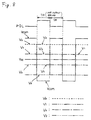
- Figure 8 shows waveforms of the gradation voltages V0 to V3, and a common electrode voltage V COM applied to a common electrode for a LCD panel.
- the gradation voltages V0 to V3 are higher in this order, and are applied to the pixels. This relationship is expressed as follows:
- the gradation voltages V0 to V3 and the common electrode voltage V COM alternately change between two voltage levels synchronously with a signal POL which is reversed for each output period.
- the common electrode voltage V COM may be d.c. voltage.
- Each level of the gradation voltages is determined to be symmetrical with respect to a given voltage (a central voltage) VM.
- Figure 9 shows each level of the gradation voltages V0 to V3 seen from a common electrode to which the common electrode voltage V COM is applied.
- a particular pixel is charged with one of the gradation voltages shown in Figure 9 when the pixel is selected by a gate driver (a scanning driver). If the pixel is selected at a beginning of a horizontal period when the gradation voltage is positive (i.e. the gradetion voltage is higher than the common electrode voltage V COM ) and the positive gradation voltage is applied to the selected pixel during the horizontal period, then it is controlled so that a negative gradation voltage (i.e. the gradation voltage is lower than the common electrode voltage V COM ) corresponding to the positive voltage is applied to the selected pixel during the next horizontal period.
- a gate driver a scanning driver
- each pixel is changed with the gradation voltage which alternately changes between a positive voltage level and a negative voltage level, that is, an a.c. voltage, resulting in preventing a d.c. voltage from being applied to the pixel as an average value.
- V S - V S ' C gd ⁇ (V GH - V GL )/(C LC + C S + C gd )
- V S - V s ' is observed as a variation of the pixel characteristics caused by the application of a positive and a negative gradation voltages to the pixels, when the positive and negative gradation voltages are actually applied to the driving terminal of a LCD panel.
- some of d.c. voltage components are applied to the pixels in a LCD panel according to the driving voltages shown in Figure 8, which is described below in more detail.
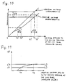
- Figure 10 shows an exemplary relationship between a gradation voltage (an absolute value) input to a LCD panel and transmissivity characteristics of the pixels in a LCD panel.
- the gradation voltage is applied to the driving terminal of a LCD panel.
- a scale of the horizontal axis is determined so that a relationship between on absolute value of a negative gradation voltage and the transmissivity characteristics is represented as a straight line.
- V N + and V N ⁇ represent positive gradation voltages and negative gradation voltages which are required to achieve the same transmissivity characteristics of pixels in a LCD panel respectively.
- V3+ and V3 ⁇ , as well as V0+ and V0 ⁇ , which are required to achieve the same transmissivity characteristics of the pixel in a LCD panel are shown in Figure 10.
- the positive and negative voltages are defined by the differences between the gradation voltages V N and the common electrode voltage V COM , as mentioned above.
- ⁇ V N represents a difference between the voltages V N + and V N ⁇ .
- Figure 11 shows a relationship between a negative gradation voltage (an absolute value) applied to the driving terminal of a LCD panel and the difference ⁇ V N .
- Figure 11 teaches that a positive gradation voltage V N + should be substantially equal to a voltage obtained by adding the difference ⁇ V N to an absolute value of a negative gradation voltage V N ⁇ , in order to achieve the same transmissivity characteristics of the pixel.
- the gradation voltage is V3 (N - 3)
- V3 (N - 3)
- an absolute value of the difference between the gradation voltage V3 and the common electrode voltage V COM in Figure 9 is substantially equal to a voltage represented by V3 in Figure 10.
- a difference ⁇ t3 in the transmissivity characteristics occurs depending on which voltage is applied to a pixel, a positive gradation voltage or a negative gradation voltage, as shown in Figure 10.
- the pixel characteristics for example, the transmissivity of liquid crystal in a case where a LCD panel is used
- the pixel characteristics causes a flicker effect of the image.
- the application of a d.c. voltage to the pixels causes not only a deterioration of the display apparatus but also a so-called "after static image" problem where a static image remains visible in the display even after the static image is deleted.
- a static image is the primary mode of display, such as a terminal display device for a computer, the problem is serious.
- the drive circuit of the present invention includes a section for receiving a digital video signal, a voltage supply section for generating a common electrode voltage and a plurality of gradation voltages, each of the plurality of gradation voltages alternately changing between two voltage levels, a driving section for selecting one of the plurality of gradation voltages according to the input digital video signal and applying the selected gradation voltage to one of the pixel electrodes, and for applying a common electrode voltage to the common electrode, the common electrode voltage being shifted based on a relationship between a driving voltage input to the display panel and the transmissivity characteristics of the pixels of a display panel so that a central value of the common electrode voltage is different from central values of the gradation voltages.
- the drive circuit of the present invention includes a section for receiving a digital video signal, a voltage supply section for generating a common electrode voltage and a plurality of gradation voltages, each of the plurality of gradation voltages alternately changing between two voltage levels, a driving section for selecting one of the plurality of gradation voltages according to the input digital video signal and applying the selected gradation voltage to one of the pixel electrodes, and for applying a common electrode voltage to the common electrode, at least one of the gradation voltages being shifted based on a relationship between a driving voltage input to a display panel and the transmissivity characteristics of the pixels of the display panel so that a central value of at least one of the gradation voltages is different from one of the central values of the remaining gradation voltages.
- the invention described herein makes possible the advantages of (1) providing a drive circuit which can reduce the ratio of d.c. voltage components to be applied to the pixels, (2) providing a drive circuit which can reduce a flicker effect of the image, and (3) providing a drive circuit which can improve an "after static image" problem.
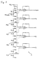
- Figure 1 is a circuit diagram showing the voltage supply section in Example 1.
- Figure 2 is a diagrammatic view showing waveforms of the gradation voltages and the common electrode voltage.
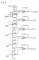
- Figure 3 is a circuit diagram showing the voltage supply section in Example 2.
- Figure 4 is a circuit diagram showing the voltage supply section in Example 3.
- Figure 5 is a circuit diagram showing an operational amplifier of the voltage supply section.
- Figure 6 is a circuit diagram showing a driving circuit for a liquid crystal display apparatus.
- Figure 7 is a circuit diagram showing a part of the driving circuit shown in Figure 6.
- Figure 8 is a diagrammatic view showing the waveforms of the gradation voltages and the common electrode voltage.
- Figure 9 is a diagrammatic view showing the waveforms of the gradation voltages and the common electrode voltage when viewed from the common electrode.
- Figure 10 is a graph showing the relationship between a voltage input to a LCD panel and a transmissivity of the pixels of a LCD panel.
- Figure 11 is a graph showing the relationship between a negative voltage input to a LCD panel and a difference between V N + and V N ⁇ .
- Figure 12 is an equivalent circuit of the pixel portion.
- FIG. 13 is an equivalent circuit wherein the switching element (TFT) is in on-state.
- FIG. 14 is an equivalent circuit wherein the switching element (TFT) is in off-state.
- Figure 15 is a circuit diagram showing the voltage supply section in Example 5.
- ⁇ V N in Figure 10 is compensated by adjusting the common electrode voltage V COM .
- Figure 2 shows waveforms of the gradation voltage V3 and the common electrode voltage V COM ' which has been adjusted based on the relationship shown in Figure 10.
- the common electrode voltage V COM is shifted so that a central value VM COM of the common electrode voltage V COM ' is different from the central voltage VM by ⁇ VM.
- a positive gradation voltage V3+ may be higher than a negative gradation voltage V3 ⁇ by ⁇ V3. This makes it possible to apply the gradation voltages V3+ and V3 ⁇ as shown in Figure 10 to the driving terminal of a LCD panel.
- Figure 1 shows an exemplary circuit for the voltage supply section 1.
- the drive circuit for a display apparatus shown in Figure 6 is exemplary of just one type of circuit which may be used in Example 1 through 5 where the voltage supply section 1 is varied.
- the present invention is not limited by this specific type of drive circuit.
- Other drive circuits may be used for the voltage supply section 1 to generate the common electrode voltage and the gradation voltages as defined by this invention.
- the circuit shown in Figure 1 includes an operational amplifier OP C for generating the common electrode voltage V COM , and operational amplifiers OP0 to OP3 for generating the gradation voltages V0 to V3.
- the operational amplifiers OP C , OP0, and OP1 receive a signal POL at their inverted inputs, and the operational amplifiers OP2 and OP3 receive the signal POL at their inverted inputs through on inverter INV.
- Each operational amplifier OP C , OP0 to OP3 receives a respective output of resistance type potential dividers PD C , PD0 to PD3 at their non-inverted inputs.
- Operational amplifiers OP C , OP0 to PO3 generate voltages V COM and V0 to V3 which alternately change between two voltage levels synchronously with the signal POL, and a central value of the two voltage levels is substantially equal to the voltage at the non-inverted inputs of each operational amplifier. Further, phases of the voltages V COM , V0 and V1 are opposite to those of the voltages V2 and V3 as shown in Figure 8. The amplitudes of these voltages depend upon the amplification factors of the operational amplifiers.
- Each resistance type potential divider PD C , and PD0 to PD3 has two fixed resistances, one being connected at one end to a power source V dd having a plus potential, and the other being connected at one end to a power source V ss having a ground potential.
- the voltage VR C at the junction of the fixed resistances R C1 and R C2 of the resistance type potential divider PD COM becomes ⁇ R C2 /(R C1 + R C2 ) ⁇ V dd .
- This voltage VR C is applied to the non-inverted input of the operational amplifier OP C as an output voltage of the resistance type potential divider PD COM .
- the voltages VR0 to VR3 at the respective junctions of the fixed resistances R01 and R02, R11 and R12, R21 and R22, and R31 and R32 become ⁇ R02/(R01 + R02) ⁇ V dd , ⁇ R12/(R11 + R12) ⁇ V dd , ⁇ R22/(R21 + R22) ⁇ V dd , and ⁇ R32/(R31 + R32) ⁇ V dd .
- the values of the output voltages VR C , VR0 to VR3 are determined by setting resistance ratios of fixed resistances.
- the central value VM COM of the output voltage V COM of the operational amplifier OP C is shifted away from the central voltage VM by ⁇ VM toward the low voltage aide.
- the central voltage VM is substantially equal to the central value of the output voltages V0 to V3 of the other operational amplifiers OP0 to OP3.
- Figure 2 shows only the voltages V COM and V3.
- the positive gradation voltage V3+ becomes substantially equal to a voltage obtained by adding the difference ⁇ VM to the voltage V3.
- the negative gradation voltage V3 ⁇ becomes substantially equal to a voltage obtained by subtracting the difference ⁇ VM from the voltage V3.
- the difference ⁇ VM con be determined by setting appropriately the output voltages VR C and VR3 (i.e. the values of the fixed resistances in the resistive potential dividers).
- the determination of the values of the fixed resistances makes it possible to obtain the voltages V3+ and V3 ⁇ which do not result in direct application of a d.c. voltage to the pixels, and keep the transmissivity constant irrespective of the positive and negative gradation voltages.
- the difference ⁇ VM may be adjusted to be an optimum value between the lines L0 and L3 in Figure 11 so that d.c. componets applied to the pixels are minimized.
- ⁇ V N in Figure 10 is compensated by adjusting the common electrode voltage V COM for each display apparatus.
- Figure 3 shows an exemplary circuit for a voltage supply section 1 used in another embodiment.
- the circuit shown in Figure 3 includes a potentiometer PM COM in place of the resistance type potential divider PD COM described in Example 1.
- a value of the output voltage VR C of the potentiometer PM COM which is applied to the non-inverted inputs of the operational amplifier OP C can be adequately adjusted. This means that the difference ⁇ VM can be adjusted so that optimum display characteristics of each display apparatus can be obtained.
- ⁇ V N in Figure 10 is compensated by adjusting the gradation voltages V0 to V3 independently.
- FIG. 4 shows an exemplary circuit for a voltage supply section 1 used in another embodiment.
- the circuit shown in Figure 4 includes potentiometers PM0 to PM3 in place of the resistance type potential dividers PD0 to PD3 set forth in Example 1. Values of the output voltages VR0 to VR3 of the potentiometer PM0 to PM3 which are applied to the non-inverted inputs of the operational amplifiers OP0 to OP3 can be independently adjusted.
- each of the gradation voltages V0 to V3 is shifted so that each central value of the gradation voltages V0 to V3 is different from the central voltage VM shown in Figure 2.
- the distance shifted away from the central voltage VM may be different among the gradation voltages V0 to V3.
- ⁇ V N in Figure 10 is compensated by adjusting the common electrode voltage V COM and the gradation voltages V0 to V3, independently.
- Figure 15 shows an exemplary circuit for the voltage supply section 1 used in another embodiment.
- the common electrode voltage V COM output from the operational amplifier OP C is a d.c. voltage. This configuration can be applied to any circuits for the voltage supply section 1 mentioned above.
- the operational amplifiers OP C , OP0 to OP3 mentioned above may have a configuration as shown in Figure 5.
- the output of the operational amplifier OP is amplified by means of a bidirectional current amplifier circuit including two transistors Q1 and Q2. This configuration can be applied to any circuits for the voltage supply section 1 mentioned above.
- the output of the current amplifier circuit are used as the common electrode voltage V COM and the gradation voltages V0 to V3, the same effect set forth can be obtained. Since a current capacity of the operational amplifier OP may be small enough to drive the transistors Q1 and Q2, it makes possible to use an operational amplifier having a small current capacity.
- the ratio of a d.c. component applied to the pixels of a LCD panel can be reduced.
- the display apparatus is not likely to be broken or deteriorated, and also the "after static image" problem can be much improved.
- the flicker effect of the image can be reduced.
- the voltages supplied by the voltage supply section 1 may be adjusted so that the flicker effect of the image be minimized.
Landscapes
- Engineering & Computer Science (AREA)
- Crystallography & Structural Chemistry (AREA)
- Chemical & Material Sciences (AREA)
- Theoretical Computer Science (AREA)
- Computer Hardware Design (AREA)
- General Physics & Mathematics (AREA)
- Physics & Mathematics (AREA)
- Power Engineering (AREA)
- Multimedia (AREA)
- Signal Processing (AREA)
- Liquid Crystal Display Device Control (AREA)
- Control Of Indicators Other Than Cathode Ray Tubes (AREA)
- Liquid Crystal (AREA)
- Picture Signal Circuits (AREA)
Applications Claiming Priority (2)
| Application Number | Priority Date | Filing Date | Title |
|---|---|---|---|
| JP211149/91 | 1991-08-22 | ||
| JP3211149A JP2912480B2 (ja) | 1991-08-22 | 1991-08-22 | 表示装置の駆動回路 |
Publications (3)
| Publication Number | Publication Date |
|---|---|
| EP0532191A2 true EP0532191A2 (fr) | 1993-03-17 |
| EP0532191A3 EP0532191A3 (en) | 1993-06-09 |
| EP0532191B1 EP0532191B1 (fr) | 1997-11-05 |
Family
ID=16601194
Family Applications (1)
| Application Number | Title | Priority Date | Filing Date |
|---|---|---|---|
| EP92307686A Expired - Lifetime EP0532191B1 (fr) | 1991-08-22 | 1992-08-21 | Circuit de commande pour un dispositif d'affichage |
Country Status (5)
| Country | Link |
|---|---|
| US (1) | US5402142A (fr) |
| EP (1) | EP0532191B1 (fr) |
| JP (1) | JP2912480B2 (fr) |
| KR (1) | KR960009443B1 (fr) |
| DE (1) | DE69223012T2 (fr) |
Cited By (5)
| Publication number | Priority date | Publication date | Assignee | Title |
|---|---|---|---|---|
| US5640174A (en) * | 1993-07-29 | 1997-06-17 | Hitachi, Ltd. | Method of driving an active matrix liquid crystal display panel with asymmetric signals |
| EP0611144A3 (fr) * | 1993-02-09 | 1997-07-30 | Sharp Kk | Circuit de génération de tension, circuit de commande d'électrode de commun, circuit de commande de ligne de signal et circuit de génération de tension de gris pour dispositifs d'affichage. |
| GB2311631A (en) * | 1993-07-21 | 1997-10-01 | Seiko Epson Corp | Controlling power supply for liquid crystal display |
| US5734379A (en) * | 1994-12-26 | 1998-03-31 | Sharp Kabushiki Kaisha | Liquid crystal display device |
| US6002384A (en) * | 1995-08-02 | 1999-12-14 | Sharp Kabushiki Kaisha | Apparatus for driving display apparatus |
Families Citing this family (27)
| Publication number | Priority date | Publication date | Assignee | Title |
|---|---|---|---|---|
| KR960008104B1 (ko) * | 1991-05-21 | 1996-06-19 | 샤프 가부시끼가이샤 | 표시장치의 구동방법과 표시장치의 구동회로 및 이를 이용한 표시장치 |
| JPH06274133A (ja) * | 1993-03-24 | 1994-09-30 | Sharp Corp | 表示装置の駆動回路及び表示装置 |
| JP3329077B2 (ja) * | 1993-07-21 | 2002-09-30 | セイコーエプソン株式会社 | 電源供給装置、液晶表示装置及び電源供給方法 |
| TW277111B (fr) * | 1994-04-20 | 1996-06-01 | Hitachi Seisakusyo Kk | |
| EP0721137B1 (fr) * | 1994-07-14 | 2004-01-21 | Seiko Epson Corporation | Circuit a sources de courant electrique, dispositif d'affichage a cristaux liquides et dispositif electronique |
| JP3275991B2 (ja) * | 1994-07-27 | 2002-04-22 | シャープ株式会社 | アクティブマトリクス型表示装置及びその駆動方法 |
| JP3106078B2 (ja) * | 1994-12-28 | 2000-11-06 | シャープ株式会社 | 液晶駆動用電源 |
| JP3322327B2 (ja) | 1995-03-14 | 2002-09-09 | シャープ株式会社 | 駆動回路 |
| JPH09152847A (ja) * | 1995-09-29 | 1997-06-10 | Sharp Corp | 液晶表示パネルの駆動方法及びその駆動回路 |
| US5867136A (en) * | 1995-10-02 | 1999-02-02 | Micron Display Technology, Inc. | Column charge coupling method and device |
| JP3471152B2 (ja) * | 1995-11-30 | 2003-11-25 | アルプス電気株式会社 | 液晶表示素子および液晶表示素子の駆動方法 |
| KR100188109B1 (ko) * | 1995-12-13 | 1999-06-01 | 김광호 | 오프전압의 레벨이 조절되는 오프전압 발생회로 |
| JP3349638B2 (ja) | 1996-11-15 | 2002-11-25 | シャープ株式会社 | 表示装置を駆動する方法および回路 |
| JP3569922B2 (ja) | 1997-03-28 | 2004-09-29 | セイコーエプソン株式会社 | 電源回路、表示装置及び電子機器 |
| KR100495801B1 (ko) * | 1997-07-23 | 2005-09-15 | 삼성전자주식회사 | 킥백전압을보상하는액정표시장치및그구동방법 |
| JP3795209B2 (ja) | 1997-12-01 | 2006-07-12 | シャープ株式会社 | 液晶表示装置及びこれに用いられる基準電位発生回路 |
| JP3813463B2 (ja) * | 2000-07-24 | 2006-08-23 | シャープ株式会社 | 液晶表示装置の駆動回路及びそれを用いた液晶表示装置並びにその液晶表示装置を用いた電子機器 |
| JP3906665B2 (ja) * | 2001-10-05 | 2007-04-18 | カシオ計算機株式会社 | 液晶駆動装置 |
| KR100438968B1 (ko) * | 2001-12-31 | 2004-07-03 | 엘지.필립스 엘시디 주식회사 | 액정 패널의 전원공급 장치 |
| KR100498542B1 (ko) * | 2002-09-06 | 2005-07-01 | 엘지.필립스 엘시디 주식회사 | 액정표시장치의 신호구동회로 및 구동방법 |
| US7940286B2 (en) * | 2004-11-24 | 2011-05-10 | Chimei Innolux Corporation | Display having controllable gray scale circuit |
| JP4813802B2 (ja) * | 2005-01-13 | 2011-11-09 | ルネサスエレクトロニクス株式会社 | 液晶駆動装置、液晶表示装置及び液晶駆動方法 |
| US20070229439A1 (en) * | 2006-03-29 | 2007-10-04 | Fansen Wang | Gamma reference voltage generating device and liquid crystal display using the same |
| US8284123B2 (en) | 2006-11-29 | 2012-10-09 | Sharp Kabushiki Kaisha | Liquid crystal display apparatus, liquid crystal display apparatus driving circuit, liquid crystal display apparatus source driver, and liquid crystal display apparatus controller |
| TWI342537B (en) * | 2006-12-11 | 2011-05-21 | Chimei Innolux Corp | Liquid crystal display device and driving method thereof |
| KR100785667B1 (ko) * | 2007-06-20 | 2007-12-14 | 주식회사 토비스 | 계조 전압별 투과율 조절 방법 및 계조 전압별 투과율을 조절할 수 있는 디스플레이 장치의 감마 전압 생성부 |
| KR101356294B1 (ko) * | 2009-11-05 | 2014-02-05 | 엘지디스플레이 주식회사 | 액정표시장치 |
Family Cites Families (15)
| Publication number | Priority date | Publication date | Assignee | Title |
|---|---|---|---|---|
| DE3019832C2 (de) * | 1979-05-28 | 1986-10-16 | Kabushiki Kaisha Suwa Seikosha, Shinjuku, Tokio/Tokyo | Treiberschaltung für eine Flüssigkristallanzeigematrix |
| JPS56117287A (en) * | 1980-02-21 | 1981-09-14 | Sharp Kk | Indicator driving system |
| KR900005489B1 (ko) * | 1984-04-26 | 1990-07-30 | 마쯔시다덴기산교 가부시기가이샤 | 액정표시장치의 구동회로 |
| JPS6211829A (ja) * | 1985-03-28 | 1987-01-20 | Toshiba Corp | アクテイブマトリツクス形液晶表示装置 |
| JPS6249399A (ja) * | 1985-08-29 | 1987-03-04 | キヤノン株式会社 | 表示装置 |
| JPS63161495A (ja) * | 1986-12-24 | 1988-07-05 | ホシデン株式会社 | 液晶駆動装置 |
| JPS63261299A (ja) * | 1987-04-17 | 1988-10-27 | 三菱電機株式会社 | アクテイブマトリクス液晶デイスプレイ用交流駆動方式 |
| US5184118A (en) * | 1987-08-13 | 1993-02-02 | Seiko Epson Corporation | Liquid crystal display apparatus and method of driving same |
| US5214417A (en) * | 1987-08-13 | 1993-05-25 | Seiko Epson Corporation | Liquid crystal display device |
| US5117298A (en) * | 1988-09-20 | 1992-05-26 | Nec Corporation | Active matrix liquid crystal display with reduced flickers |
| JPH0830798B2 (ja) * | 1988-10-19 | 1996-03-27 | シャープ株式会社 | 液晶表示装置 |
| JP2854621B2 (ja) * | 1989-09-01 | 1999-02-03 | シャープ株式会社 | 表示装置の駆動回路 |
| JP2685609B2 (ja) * | 1989-12-06 | 1997-12-03 | シャープ株式会社 | 表示装置の駆動回路 |
| JPH0383014A (ja) * | 1989-08-28 | 1991-04-09 | Toshiba Corp | 液晶表示装置の駆動方法 |
| JPH03198089A (ja) * | 1989-12-27 | 1991-08-29 | Sharp Corp | 液晶表示装置の駆動回路 |
-
1991
- 1991-08-22 JP JP3211149A patent/JP2912480B2/ja not_active Expired - Lifetime
-
1992
- 1992-08-21 DE DE69223012T patent/DE69223012T2/de not_active Expired - Lifetime
- 1992-08-21 US US07/934,389 patent/US5402142A/en not_active Expired - Lifetime
- 1992-08-21 EP EP92307686A patent/EP0532191B1/fr not_active Expired - Lifetime
- 1992-08-29 KR KR1019920015205A patent/KR960009443B1/ko not_active Expired - Lifetime
Cited By (12)
| Publication number | Priority date | Publication date | Assignee | Title |
|---|---|---|---|---|
| EP0611144A3 (fr) * | 1993-02-09 | 1997-07-30 | Sharp Kk | Circuit de génération de tension, circuit de commande d'électrode de commun, circuit de commande de ligne de signal et circuit de génération de tension de gris pour dispositifs d'affichage. |
| US5929847A (en) * | 1993-02-09 | 1999-07-27 | Sharp Kabushiki Kaisha | Voltage generating circuit, and common electrode drive circuit, signal line drive circuit and gray-scale voltage generating circuit for display devices |
| US6310616B1 (en) | 1993-02-09 | 2001-10-30 | Sharp Kabushiki Kaisha | Voltage generating circuit, and common electrode drive circuit signal line drive circuit and gray-scale voltage generating circuit for display device |
| US6509895B2 (en) | 1993-02-09 | 2003-01-21 | Sharp Kabushiki Kaisha | Voltage generating circuit, and common electrode drive circuit, signal line drive circuit and gray-scale voltage generating circuit for display devices |
| GB2311631A (en) * | 1993-07-21 | 1997-10-01 | Seiko Epson Corp | Controlling power supply for liquid crystal display |
| GB2311630A (en) * | 1993-07-21 | 1997-10-01 | Seiko Epson Corp | Controlling power supply for liquid crystal display |
| GB2311631B (en) * | 1993-07-21 | 1997-11-12 | Seiko Epson Corp | Power supply device |
| GB2311630B (en) * | 1993-07-21 | 1997-11-12 | Seiko Epson Corp | Power supply device |
| US5640174A (en) * | 1993-07-29 | 1997-06-17 | Hitachi, Ltd. | Method of driving an active matrix liquid crystal display panel with asymmetric signals |
| US5734379A (en) * | 1994-12-26 | 1998-03-31 | Sharp Kabushiki Kaisha | Liquid crystal display device |
| CN1129887C (zh) * | 1994-12-26 | 2003-12-03 | 夏普公司 | 液晶显示装置 |
| US6002384A (en) * | 1995-08-02 | 1999-12-14 | Sharp Kabushiki Kaisha | Apparatus for driving display apparatus |
Also Published As
| Publication number | Publication date |
|---|---|
| KR960009443B1 (ko) | 1996-07-19 |
| EP0532191A3 (en) | 1993-06-09 |
| JPH0553534A (ja) | 1993-03-05 |
| US5402142A (en) | 1995-03-28 |
| JP2912480B2 (ja) | 1999-06-28 |
| KR930004918A (ko) | 1993-03-23 |
| DE69223012D1 (de) | 1997-12-11 |
| DE69223012T2 (de) | 1998-04-23 |
| EP0532191B1 (fr) | 1997-11-05 |
Similar Documents
| Publication | Publication Date | Title |
|---|---|---|
| EP0532191B1 (fr) | Circuit de commande pour un dispositif d'affichage | |
| US6359608B1 (en) | Method and apparatus for driving flat screen displays using pixel precharging | |
| US6392626B1 (en) | Liquid crystal display having different common voltages | |
| US4591848A (en) | Matrix panel with an active driving system | |
| KR100188112B1 (ko) | 박막 트랜지스터 액정 표시 장치 | |
| US5537129A (en) | Common electrode driving circuit for use in a display apparatus | |
| US6600472B1 (en) | Liquid crystal display device | |
| KR100777705B1 (ko) | 액정 표시 장치 및 그 구동 방법 | |
| US6600465B1 (en) | Driver circuit for active matrix display | |
| JP4001948B2 (ja) | ビデオ表示装置 | |
| EP0196889A2 (fr) | Dispositif d'affichage à cristaux liquides adressé en matrice | |
| EP0199361B1 (fr) | Circuit de commande pour un dispositif d'affichage à cristaux liquides | |
| JP3863214B2 (ja) | ビデオ信号供給装置 | |
| EP0588398B1 (fr) | Dispositifs d'affichage à matrice active et leur procédé de commande | |
| EP0436384B1 (fr) | Circuit de commande pour un dispositif d'affichage à cristaux liquides | |
| JPH11509937A (ja) | アクティブマトリックス液晶ディスプレイ用集積化アナログソースドライバ | |
| KR100205259B1 (ko) | 액티브매트릭스 액정디스플레이의 구동회로 | |
| JPH06138841A (ja) | アクティブマトリックスフラットディスプレイ | |
| CA1261490A (fr) | Circuit d'excitation pour affichage a cristal liquide | |
| JPH067232B2 (ja) | 液晶表示装置 | |
| EP0600609A1 (fr) | Circuit de commande pour un dispositif d'affichage | |
| KR100864491B1 (ko) | 액정 표시 장치의 구동 장치 | |
| EP0434465B1 (fr) | Circuit de commande pour un dispositif d'affichage à cristaux liquides | |
| EP0544427B1 (fr) | Circuit de contrÔle pour un système d'affichage avec un circuit d'attaque de source numérique, capable de générer des tensions d'attaque à plusieurs niveaux en partant d'une seule source d'énergie externe | |
| JP2965822B2 (ja) | 電源回路 |
Legal Events
| Date | Code | Title | Description |
|---|---|---|---|
| PUAI | Public reference made under article 153(3) epc to a published international application that has entered the european phase |
Free format text: ORIGINAL CODE: 0009012 |
|
| AK | Designated contracting states |
Kind code of ref document: A2 Designated state(s): DE FR GB NL |
|
| PUAL | Search report despatched |
Free format text: ORIGINAL CODE: 0009013 |
|
| AK | Designated contracting states |
Kind code of ref document: A3 Designated state(s): DE FR GB NL |
|
| 17P | Request for examination filed |
Effective date: 19930826 |
|
| 17Q | First examination report despatched |
Effective date: 19950704 |
|
| GRAG | Despatch of communication of intention to grant |
Free format text: ORIGINAL CODE: EPIDOS AGRA |
|
| GRAH | Despatch of communication of intention to grant a patent |
Free format text: ORIGINAL CODE: EPIDOS IGRA |
|
| GRAH | Despatch of communication of intention to grant a patent |
Free format text: ORIGINAL CODE: EPIDOS IGRA |
|
| GRAA | (expected) grant |
Free format text: ORIGINAL CODE: 0009210 |
|
| AK | Designated contracting states |
Kind code of ref document: B1 Designated state(s): DE FR GB NL |
|
| REF | Corresponds to: |
Ref document number: 69223012 Country of ref document: DE Date of ref document: 19971211 |
|
| ET | Fr: translation filed | ||
| PLBE | No opposition filed within time limit |
Free format text: ORIGINAL CODE: 0009261 |
|
| STAA | Information on the status of an ep patent application or granted ep patent |
Free format text: STATUS: NO OPPOSITION FILED WITHIN TIME LIMIT |
|
| 26N | No opposition filed | ||
| REG | Reference to a national code |
Ref country code: GB Ref legal event code: IF02 |
|
| PGFP | Annual fee paid to national office [announced via postgrant information from national office to epo] |
Ref country code: FR Payment date: 20110818 Year of fee payment: 20 Ref country code: DE Payment date: 20110817 Year of fee payment: 20 Ref country code: GB Payment date: 20110817 Year of fee payment: 20 |
|
| PGFP | Annual fee paid to national office [announced via postgrant information from national office to epo] |
Ref country code: NL Payment date: 20110823 Year of fee payment: 20 |
|
| REG | Reference to a national code |
Ref country code: DE Ref legal event code: R071 Ref document number: 69223012 Country of ref document: DE |
|
| REG | Reference to a national code |
Ref country code: DE Ref legal event code: R071 Ref document number: 69223012 Country of ref document: DE |
|
| REG | Reference to a national code |
Ref country code: NL Ref legal event code: V4 Effective date: 20120821 |
|
| REG | Reference to a national code |
Ref country code: GB Ref legal event code: PE20 Expiry date: 20120820 |
|
| PG25 | Lapsed in a contracting state [announced via postgrant information from national office to epo] |
Ref country code: GB Free format text: LAPSE BECAUSE OF EXPIRATION OF PROTECTION Effective date: 20120820 Ref country code: DE Free format text: LAPSE BECAUSE OF EXPIRATION OF PROTECTION Effective date: 20120822 |