EP0532295A2 - Circuit de correction de l'échelle des gris - Google Patents
Circuit de correction de l'échelle des gris Download PDFInfo
- Publication number
- EP0532295A2 EP0532295A2 EP92308182A EP92308182A EP0532295A2 EP 0532295 A2 EP0532295 A2 EP 0532295A2 EP 92308182 A EP92308182 A EP 92308182A EP 92308182 A EP92308182 A EP 92308182A EP 0532295 A2 EP0532295 A2 EP 0532295A2
- Authority
- EP
- European Patent Office
- Prior art keywords
- circuit
- output
- video signal
- cumulative histogram
- normalizing
- Prior art date
- Legal status (The legal status is an assumption and is not a legal conclusion. Google has not performed a legal analysis and makes no representation as to the accuracy of the status listed.)
- Withdrawn
Links
Images


Classifications
-
- G—PHYSICS
- G06—COMPUTING OR CALCULATING; COUNTING
- G06T—IMAGE DATA PROCESSING OR GENERATION, IN GENERAL
- G06T5/00—Image enhancement or restoration
- G06T5/90—Dynamic range modification of images or parts thereof
- G06T5/92—Dynamic range modification of images or parts thereof based on global image properties
-
- G—PHYSICS
- G06—COMPUTING OR CALCULATING; COUNTING
- G06T—IMAGE DATA PROCESSING OR GENERATION, IN GENERAL
- G06T5/00—Image enhancement or restoration
- G06T5/40—Image enhancement or restoration using histogram techniques
-
- H—ELECTRICITY
- H04—ELECTRIC COMMUNICATION TECHNIQUE
- H04N—PICTORIAL COMMUNICATION, e.g. TELEVISION
- H04N5/00—Details of television systems
- H04N5/14—Picture signal circuitry for video frequency region
- H04N5/20—Circuitry for controlling amplitude response
Definitions
- This invention relates to a gray level correction circuit for effective use of the cathode ray tube with a small dynamic range.
- Fig. 3 shows the arrangement of a conventional gray level correction circuit.
- reference numeral 1 denotes a cumulative histogram circuit for forming a cumulative histogram of each field of the input video signal, and outputting a result "a".
- the numeral 3 denotes a normalizing circuit for normalizing output of the cumulative histogram circuit 1 by dividing it by the number of samples hitherto included.
- the numeral 4 denotes an interpolation circuit for outputting a correction value for each pixel.
- the numeral 5 denotes a multiplier circuit for multiplying the output of the interpolation circuit 4 by a constant.
- the numeral 6 denotes an adder circuit for adding the output of the multiplier circuit 5 to the input video signal.
- the cumulative histogram circuit 1 forms a cumulative histogram of each field of the input video signal, and outputs a result "a".
- Fig. 4 shows samples distributed from level 0 to level 128 in the case where an input signal is an 8-bit signal which can represents any of 256 levels of tone.
- the sample number M at level 255 is a total number of samples because the graph is a cumulative histogram.
- the normalizing circuit 3 divides the result "a" of the histogram by the total number of samples, and outputs "c".
- data used here is output by 8-bit signals.
- the normalized signal "c" is input to the interpolation circuit 4, which subtracts an input signal from the cumulative histogram normalized for each pixel of the input video signal, and outputs a correction value "d” for each pixel.
- the multiplier 5 multiplies the correction value "d” by a constant to decide a correction amount, and outputs a correction signal "e”.
- the constant used in Fig. 4 is 1/2.
- the adder circuit 6 adds the input signal and the correction signal "e” together, and supplies output "f".
- the present invention provides a gray level correction circuit capable of performing a specified correction on the video signal which has passed the contrast circuit without the picture becoming whitish at any value of contrast.
- the gray level correction circuit comprises a cumulative histogram circuit for forming a cumulative histogram for each field, a first multiplier for multiplying an output signal of the cumulative histogram circuit by a constant corresponding to a value of contrast, a normalizing circuit for normalizing output of the first multiplier by dividing it by the total number of samples, an interpolation circuit for outputting a correction value for each pixel according to output of the normalizing circuit and the input video signal, a second multiplier for multiplying the correction value by a constant, and an adder circuit for adding a correction value supplied from the second multiplier to the video signal.
- the gray level correction circuit according to the present invention can perform an intended correction because it can prevent the picture from becoming whitish by multiplying the output signal of the cumulative histogram circuit by a constant corresponding to the value of contrast and then supplying the multiplication result to the normalizing circuit.
- the present invention makes it possible to perform a gray level correction on the video signal, even when the video signal has passed the contrast circuit, in the manner as originally intended without making the picture whitish at any value of contrast.
- the present invention provides a great effect in practical application.
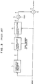
- Fig. 1 is a block diagram showing the arrangement of the gray level correction circuit according to the present invention.
- the numeral 1 denotes a cumulative histogram circuit for forming a cumulative histogram for each field of the input video signal, and outputting a result "a".
- the numeral 2 denotes a first multiplier circuit for multiplying output "a" of the cumulative histogram circuit 1 by a first constant.
- the numeral 3 denotes a normalizing circuit for normalizing the output "b" of of the first multiplier circuit by the total number of samples, and outputting "c”.
- the numeral 4 denotes an interpolation circuit for outputting a correction value for each pixel according to output "c" of the normalizing circuit 3 and the input video signal.
- the reference numeral 5 denotes a second multiplier circuit for multiplying output "d” of the interpolation circuit 4 by a second constant.
- the numeral 6 denotes an adder circuit for adding output of the adder circuit 5 to the input video signal.
- the cumulative histogram circuit 1 forms a cumulative histogram for each field of the input video signal, and outputs a result "a".
- Fig. 2 shows a case where an input signal having eight bits is used so as to represent 256 levels of tone, and the samples are distributed from level 0 to level 128. Since these are histograms, the sample number M at level 255 is the total number of samples.
- the first multiplier circuit 2 multiplies the output signal of the cumulative histogram circuit 1 by a constant corresponding to the value of contrast, and outputs "b". In Fig. 2, the constant used here is 1/2.
- the normalizing circuit 3 normalizes the result "a" of histogram by dividing it by the total number of samples, and outputs "c".
- the output "c" here is an 8-bit signal.
- the normalized signal "c” is input to the interpolation circuit 4, which subtracts the input signal from the cumulative histogram normalized for each pixel of the input video signal, and outputs a correction value "d" for each pixel.
- the second multiplier 5 decides a correction amount by multiplying "d” by a constant, and outputs a correction signal "e”.
- the constant used at this step is 1/2.
- the adder circuit 6 adds the input signal and the correction signal "e” together, and outputs a signal "f".
Landscapes
- Engineering & Computer Science (AREA)
- Physics & Mathematics (AREA)
- General Physics & Mathematics (AREA)
- Theoretical Computer Science (AREA)
- Multimedia (AREA)
- Signal Processing (AREA)
- Picture Signal Circuits (AREA)
- Transforming Electric Information Into Light Information (AREA)
- Controls And Circuits For Display Device (AREA)
Applications Claiming Priority (2)
| Application Number | Priority Date | Filing Date | Title |
|---|---|---|---|
| JP3229972A JPH0566751A (ja) | 1991-09-10 | 1991-09-10 | 階調補正回路 |
| JP229972/91 | 1991-09-10 |
Publications (2)
| Publication Number | Publication Date |
|---|---|
| EP0532295A2 true EP0532295A2 (fr) | 1993-03-17 |
| EP0532295A3 EP0532295A3 (en) | 1993-08-11 |
Family
ID=16900595
Family Applications (1)
| Application Number | Title | Priority Date | Filing Date |
|---|---|---|---|
| EP19920308182 Withdrawn EP0532295A3 (en) | 1991-09-10 | 1992-09-09 | Gray scale correction circuit |
Country Status (3)
| Country | Link |
|---|---|
| EP (1) | EP0532295A3 (fr) |
| JP (1) | JPH0566751A (fr) |
| KR (1) | KR960008393B1 (fr) |
Cited By (3)
| Publication number | Priority date | Publication date | Assignee | Title |
|---|---|---|---|---|
| GB2281674A (en) * | 1993-09-03 | 1995-03-08 | Matsushita Electric Industrial Co Ltd | Digital image contrast conversion |
| EP0648043A1 (fr) * | 1993-10-08 | 1995-04-12 | Koninklijke Philips Electronics N.V. | Circuit d'amélioration du signal d'image |
| WO1997049064A1 (fr) * | 1996-06-20 | 1997-12-24 | Samsung Electronics Co., Ltd. | Dispositif d'egalisation d'histogrammes renforçant le contraste d'une image animee et procede associe |
Families Citing this family (7)
| Publication number | Priority date | Publication date | Assignee | Title |
|---|---|---|---|---|
| US6373533B1 (en) | 1997-03-06 | 2002-04-16 | Matsushita Electric Industrial Co., Ltd. | Image quality correction circuit for video signals |
| US6038341A (en) * | 1997-03-06 | 2000-03-14 | Matsushita Electric Industrial Co., Ltd. | Histogram operating unit for video signals |
| JP2951909B2 (ja) * | 1997-03-17 | 1999-09-20 | 松下電器産業株式会社 | 撮像装置の階調補正装置及び階調補正方法 |
| JP2951910B2 (ja) * | 1997-03-18 | 1999-09-20 | 松下電器産業株式会社 | 撮像装置の階調補正装置及び階調補正方法 |
| JP4278317B2 (ja) | 2001-07-05 | 2009-06-10 | 富士通マイクロエレクトロニクス株式会社 | 演算装置および受信装置 |
| KR100437807B1 (ko) * | 2002-01-21 | 2004-06-30 | 엘지전자 주식회사 | 히스토그램 평탄화 방법 및 장치 |
| CN113411511B (zh) * | 2021-06-29 | 2022-05-17 | 中国科学院长春光学精密机械与物理研究所 | 基于直方图分析的高帧频成像系统图像预处理方法 |
Family Cites Families (2)
| Publication number | Priority date | Publication date | Assignee | Title |
|---|---|---|---|---|
| US4642683A (en) * | 1985-05-06 | 1987-02-10 | Eastman Kodak Company | Digital image processing method for images with bimodal tone value distribution |
| JPH0787587B2 (ja) * | 1990-02-16 | 1995-09-20 | 松下電器産業株式会社 | 階調補正装置 |
-
1991
- 1991-09-10 JP JP3229972A patent/JPH0566751A/ja active Pending
-
1992
- 1992-09-08 KR KR1019920016363A patent/KR960008393B1/ko not_active Expired - Fee Related
- 1992-09-09 EP EP19920308182 patent/EP0532295A3/en not_active Withdrawn
Cited By (8)
| Publication number | Priority date | Publication date | Assignee | Title |
|---|---|---|---|---|
| GB2281674A (en) * | 1993-09-03 | 1995-03-08 | Matsushita Electric Industrial Co Ltd | Digital image contrast conversion |
| GB2281674B (en) * | 1993-09-03 | 1997-11-05 | Matsushita Electric Industrial Co Ltd | Digital image processing apparatus |
| US6442294B1 (en) | 1993-09-03 | 2002-08-27 | Matsushita Electric Industrial Co., Ltd. | Digital image processing apparatus with interpolation and adder circuits |
| EP0648043A1 (fr) * | 1993-10-08 | 1995-04-12 | Koninklijke Philips Electronics N.V. | Circuit d'amélioration du signal d'image |
| BE1007608A3 (nl) * | 1993-10-08 | 1995-08-22 | Philips Electronics Nv | Beeldsignaalverbeteringsschakeling. |
| US5734746A (en) * | 1993-10-08 | 1998-03-31 | U.S. Philips Corporation | Picture signal enhancement circuit includes a non-linear circuit for enhancing the picture signal in dependence of histograms measured at transitions in the picture signal |
| WO1997049064A1 (fr) * | 1996-06-20 | 1997-12-24 | Samsung Electronics Co., Ltd. | Dispositif d'egalisation d'histogrammes renforçant le contraste d'une image animee et procede associe |
| GB2321817A (en) * | 1996-06-20 | 1998-08-05 | Samsung Electronics Co Ltd | A histogram equalization apparatus for contrast enhancement of moving image and method therefor |
Also Published As
| Publication number | Publication date |
|---|---|
| KR930007261A (ko) | 1993-04-22 |
| KR960008393B1 (ko) | 1996-06-26 |
| EP0532295A3 (en) | 1993-08-11 |
| JPH0566751A (ja) | 1993-03-19 |
Similar Documents
| Publication | Publication Date | Title |
|---|---|---|
| US20050226526A1 (en) | Image processing device and method | |
| EP0630160A2 (fr) | Contrôle dynamique du contraste par la correction | |
| EP0442369B1 (fr) | Circuit de correction de gradation | |
| EP0966165A1 (fr) | Circuit de traitement de signal video délivrant un niveau de signal optimal pour la correction inverse de gamma | |
| EP0784399A1 (fr) | Dispositif de prise de vues | |
| EP0133586A1 (fr) | Appareil et procédé pour produire un signal vidéo d'image stationnaire utilisant un dispositif d'image à corps solide | |
| EP1237360B1 (fr) | Dispositif de correction de contour | |
| EP0532295A2 (fr) | Circuit de correction de l'échelle des gris | |
| US5296941A (en) | Gradation compensation apparatus of video image | |
| US6822625B2 (en) | Image processing device | |
| US6661917B1 (en) | Gradation correcting apparatus | |
| US5162925A (en) | Color image processor capable of performing masking using a reduced number of bits | |
| JP4289225B2 (ja) | 画像処理装置および画像処理方法 | |
| JP3255258B2 (ja) | 画像表示装置 | |
| US7391480B2 (en) | Image processing apparatus and image processing method for performing gamma correction | |
| JP3080019B2 (ja) | 映像信号処理装置 | |
| JP2929983B2 (ja) | カラー画像処理装置 | |
| JP2590931B2 (ja) | 信号補正回路 | |
| EP0604759A1 (fr) | Procédé et appareil pour traiter des données digitales d'image | |
| JPH0690382A (ja) | 階調補正装置 | |
| JPH0818826A (ja) | ディジタルガンマ補正回路 | |
| JP2843912B2 (ja) | 画像処理方法 | |
| JP4285117B2 (ja) | 映像信号処理装置,映像信号処理方法及び映像表示装置 | |
| JPH08163579A (ja) | 輝度補正回路 | |
| KR970073039A (ko) | 밝기보상기능을 가진 평균 분리 히스토그램 등화를 이용한 화질 개선방법과 그 회로 |
Legal Events
| Date | Code | Title | Description |
|---|---|---|---|
| PUAI | Public reference made under article 153(3) epc to a published international application that has entered the european phase |
Free format text: ORIGINAL CODE: 0009012 |
|
| AK | Designated contracting states |
Kind code of ref document: A2 Designated state(s): DE FR GB IT |
|
| PUAL | Search report despatched |
Free format text: ORIGINAL CODE: 0009013 |
|
| AK | Designated contracting states |
Kind code of ref document: A3 Designated state(s): DE FR GB IT |
|
| 17P | Request for examination filed |
Effective date: 19940113 |
|
| 17Q | First examination report despatched |
Effective date: 19940601 |
|
| 18D | Application deemed to be withdrawn |
Effective date: 19980210 |