EP0533497A2 - Procédé de gravure sèche - Google Patents
Procédé de gravure sèche Download PDFInfo
- Publication number
- EP0533497A2 EP0533497A2 EP92308553A EP92308553A EP0533497A2 EP 0533497 A2 EP0533497 A2 EP 0533497A2 EP 92308553 A EP92308553 A EP 92308553A EP 92308553 A EP92308553 A EP 92308553A EP 0533497 A2 EP0533497 A2 EP 0533497A2
- Authority
- EP
- European Patent Office
- Prior art keywords
- etching
- gaas
- layer
- photo
- light
- Prior art date
- Legal status (The legal status is an assumption and is not a legal conclusion. Google has not performed a legal analysis and makes no representation as to the accuracy of the status listed.)
- Withdrawn
Links
Images


Classifications
-
- H—ELECTRICITY
- H10—SEMICONDUCTOR DEVICES; ELECTRIC SOLID-STATE DEVICES NOT OTHERWISE PROVIDED FOR
- H10P—GENERIC PROCESSES OR APPARATUS FOR THE MANUFACTURE OR TREATMENT OF DEVICES COVERED BY CLASS H10
- H10P50/00—Etching of wafers, substrates or parts of devices
- H10P50/20—Dry etching; Plasma etching; Reactive-ion etching
- H10P50/24—Dry etching; Plasma etching; Reactive-ion etching of semiconductor materials
- H10P50/246—Dry etching; Plasma etching; Reactive-ion etching of semiconductor materials of Group III-V materials
-
- H—ELECTRICITY
- H10—SEMICONDUCTOR DEVICES; ELECTRIC SOLID-STATE DEVICES NOT OTHERWISE PROVIDED FOR
- H10D—INORGANIC ELECTRIC SEMICONDUCTOR DEVICES
- H10D10/00—Bipolar junction transistors [BJT]
- H10D10/01—Manufacture or treatment
- H10D10/021—Manufacture or treatment of heterojunction BJTs [HBT]
-
- H—ELECTRICITY
- H10—SEMICONDUCTOR DEVICES; ELECTRIC SOLID-STATE DEVICES NOT OTHERWISE PROVIDED FOR
- H10D—INORGANIC ELECTRIC SEMICONDUCTOR DEVICES
- H10D30/00—Field-effect transistors [FET]
- H10D30/01—Manufacture or treatment
- H10D30/015—Manufacture or treatment of FETs having heterojunction interface channels or heterojunction gate electrodes, e.g. HEMT
-
- H—ELECTRICITY
- H10—SEMICONDUCTOR DEVICES; ELECTRIC SOLID-STATE DEVICES NOT OTHERWISE PROVIDED FOR
- H10D—INORGANIC ELECTRIC SEMICONDUCTOR DEVICES
- H10D64/00—Electrodes of devices having potential barriers
- H10D64/01—Manufacture or treatment
- H10D64/012—Manufacture or treatment of electrodes comprising a Schottky barrier to a semiconductor
- H10D64/0124—Manufacture or treatment of electrodes comprising a Schottky barrier to a semiconductor to Group III-V semiconductors
- H10D64/0125—Manufacture or treatment of electrodes comprising a Schottky barrier to a semiconductor to Group III-V semiconductors characterised by the sectional shape, e.g. T or inverted T
-
- H—ELECTRICITY
- H10—SEMICONDUCTOR DEVICES; ELECTRIC SOLID-STATE DEVICES NOT OTHERWISE PROVIDED FOR
- H10P—GENERIC PROCESSES OR APPARATUS FOR THE MANUFACTURE OR TREATMENT OF DEVICES COVERED BY CLASS H10
- H10P14/00—Formation of materials, e.g. in the shape of layers or pillars
- H10P14/60—Formation of materials, e.g. in the shape of layers or pillars of insulating materials
- H10P14/63—Formation of materials, e.g. in the shape of layers or pillars of insulating materials characterised by the formation processes
- H10P14/6302—Non-deposition formation processes
- H10P14/6304—Formation by oxidation, e.g. oxidation of the substrate
- H10P14/6306—Formation by oxidation, e.g. oxidation of the substrate of the semiconductor materials
-
- H—ELECTRICITY
- H10—SEMICONDUCTOR DEVICES; ELECTRIC SOLID-STATE DEVICES NOT OTHERWISE PROVIDED FOR
- H10P—GENERIC PROCESSES OR APPARATUS FOR THE MANUFACTURE OR TREATMENT OF DEVICES COVERED BY CLASS H10
- H10P50/00—Etching of wafers, substrates or parts of devices
- H10P50/69—Etching of wafers, substrates or parts of devices using masks for semiconductor materials
- H10P50/691—Etching of wafers, substrates or parts of devices using masks for semiconductor materials for Group V materials or Group III-V materials
- H10P50/692—Etching of wafers, substrates or parts of devices using masks for semiconductor materials for Group V materials or Group III-V materials characterised by their composition, e.g. multilayer masks or materials
-
- H—ELECTRICITY
- H10—SEMICONDUCTOR DEVICES; ELECTRIC SOLID-STATE DEVICES NOT OTHERWISE PROVIDED FOR
- H10D—INORGANIC ELECTRIC SEMICONDUCTOR DEVICES
- H10D62/00—Semiconductor bodies, or regions thereof, of devices having potential barriers
- H10D62/80—Semiconductor bodies, or regions thereof, of devices having potential barriers characterised by the materials
- H10D62/85—Semiconductor bodies, or regions thereof, of devices having potential barriers characterised by the materials being Group III-V materials, e.g. GaAs
Definitions
- the present invention relates to a dry etching method, and particularly, to a dry etching method capable of selectively etching the desired material from a plurality of materials having different types of band gap energies or from a plurality of materials having different band gap energies.
- the technique of selectively etching the desired material from a plurality of semiconductors having different compositions is very important in fabrication of a compound semiconductor device. For example, in fabrication of a semiconductor device having a heterostructure of GaAs and Al x Ga l - x As, Al x Ga l - x As is selectively etched by wet etching and GaAs is selectively etched by dry etching.
- the selective wet etching of Al x Ga l - x As is conducted using an etchant of HCl/H2O2 or NH3/H2O2/H2O. This is utilized in fabrication of a laser diode, HBT(Hetero- Bipolar Transistor) and the like.
- HBT Hetero- Bipolar Transistor
- the wet etching has such a problem as causing an under-cut and is thus unsuitable for fine patterning.
- the present invention has been made, and the object is to provide a method for selectively etching Al x Ga l - x As to GaAs.
- a wider object is to provide a method of selectively etching among different materials generally.
- a method for selectively etching Al x Ga l - x As to GaAs by irradiating a light on a sample to be etched for changing an etching rate ratio between Al x Ga l - x As and GaAs.
- the present invention has realized the selective etching of Al x Ga l - x As to GaAs, for example, by utilizing the difference in a photo-absorbing characteristic between Al x Ga l - x As and GaAs.
- Al x Ga l - x As is variable in the transition type and the band gap energy Eg (Al x Ga l - x As) depending on the composition (x).
- Fig. 15 shows a relationship between the composition and the band gap energy.
- the relationship between the Eg (Al x Ga l - x As) and Eg (GaAs) is represented as follows: Eg (GaAs) ⁇ Eg (Al x Ga l-x As)
- the light having such a wavelength as satisfying the equation (5) can induce the strong photo-reaction on the surface of GaAs.
- GaAs film on GaAs substrate it is possible to promote the film forming reaction through the photo-absorption by a substrate.
- the reason for this is that electrons and positive holes photo-excited on the surface of GaAs react with a source gas molecules absorbed on the surface of GaAs.
- Al x Ga l-x As has a small photo-absorption coefficient as compared with GaAs, the film formation by the photoabsorption of the substrate is retarded as compared with GaAs.
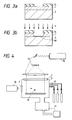
- a source gas for forming GaAs is introduced into an etching chamber, and a light 4 having such a wavelength as satisfying the above equation (2), that is, capable of being absorbed by only GaAs is irradiated on the sample. Consequently, the etching rate is retarded on the surface of the GaAs 2 because the etching reaction and the film formation due to the photo-CVD reaction of GaAs are competed with each other. Meanwhile, only the etching reaction is progressed on the surface of the Al x Ga l-x As 1.
- the Al x Ga l-x As 1 is selectively etched as shown in Fig. 1b, and the etching rate of GaAs is significantly small.
- the portion 5 of GaAs formed by the photo-CVD reaction is emphasized.
- various conditions are adjusted such that the photo-CVD reaction and the etching reaction of GaAs are cancelled to each other so as to generate the least possible film formation and the etching.
- a light as satisfying the above equation (3) that is, capable of being absorbed by Al x Ga l-x As may be used as an irradiated light.
- the reason for this is that, even in the light having such a wavelength, the photo-absorption coefficient of GaAs is larger than Al x Ga l-x As.
- the etching reaction tends to be obstructed and retarded by an oxide film formed on the surface of a sample.
- the sticking coefficient of O2 is made larger several times. This is seemed to be related to the carriers generated on the GaAs surface.
- the oxide film equivalent to one molecular layer is formed on the GaAs surface.
- oxygen other than the etching gas is introduced in the etching chamber, and the etching is conducted by irradiating the light having the wavelength satisfying the equation (2), that is, capable of being absorbed by only GaAs, so that the surface of the GaAs 1 is covered with a thin guide film for obstructing the etching reaction, resulting in the retarded etching rate.
- the selective etching of the Al x Ga l-x As 1 is possible to the GaAs 2.
- the oxide of A1 is low in its vapor pressure as compared with the oxide of Ga which may significantly obstruct the etching reaction of the Al x Ga l-x As. Accordingly, in using the light having the wavelength satisfying the equation (3), it is desired to select the light of the longer wavelength.
- the photo-stimulated desorption is induced by a thermal mechanism by heating of the substrate, and an electronic mechanism by the electronic kinetics through excitation of electronic state of the absorbing material or the substrate.
- the electronic kinetics through excitation of electronic state of the substrate is related.
- the electrons excited to the empty level above the Fermi energy are elastically tunneled to the empty level of the absorbed gas molecules, which promotes the stimulated desorption of the absorbed molecules. Accordingly, when the etching gas is absorbed and is reacted with the surface, by promotion of the stimulated desorption being reversed to the absorption, the absorbed gas can be desorbed before being reacted with the substrate, resulting in the retarded etching reaction.
- the sample including an Al x Ga l-x As 1 and a GaAs 2 as shown in Fig. 1a when the light capable of being absorbed by only GaAs is irradiated, the stimulated desorption of the absorbed etching gas is promoted on the GaAs surface thereby reducing the etching rate, which enables the selective etching of Al x Ga l-x As to GaAs.
- the chemical reaction mainly dominates the dry etching, the utilization of the photo-stimulated desorption is particularly effective.
- a light satisfying the equation (3) that is, capable of being absorbed by Al x Ga l-x As may be used as the irradiated light. This is because, even in the light having such a wavelength, the photo-absorption coefficient of GaAs is larger than Al x Ga l-x As.
- the present invention has been explained regarding the selective etching of Al x Ga l-x As to GaAs, it is applicable for the whole selective etching of the material having the smaller photo-absorption among the materials having different photo-absorption characteristics.
- the types of band gap energies for the main semiconductors are shown in Table 1. By suitable combination of the materials as shown in Table 1, the selective etching is possible by easily applying the present invention.
- the etching in a sample having an composition continuously variable in the thickness direction, that is, a graded composition, the etching can be stopped at the depth having the specified composition.
- the band gap energy of the direct transition is represented in the following equation (6) as a function Eg(x)[eV] of the composition (x) of Al.
- Eg (x) 1.439 + 1.042 x + 0.468 x2
- the value of Eg on the surface of the sample becomes smaller gradually.
- the etching may be conducted while irradiating the light having a wavelength ⁇ o represented in the equation (7) on the sample.
- ⁇ 0 h c Eg(Al x0 Ga l-x 0 As)
- the photo-CVD reaction is utilized.
- RIE Reactive Ion Etching
- TMGa Ga (CH3)3 trimethylgallium
- AsH3(arsine) are used as a source gas for forming GaAs
- a low pressure mercury lamp is used as a light source of photo-CVD.
- FIG. 2 An equipment used in this Example is shown in Fig. 2.
- the ground electrode of the conventional RIE equipment is replaced into a meshly ground electrode 8, and a light from a low pressure mercury lamp 6 can be irradiated to a sample 11 through a fused quartz window 7.
- the low pressure mercury lamp 6 emits an ultra-violet light having a wavelength of 185nm and 245nm. It is sufficiently shorter than the wavelength of the photon corresponding to the energy of the band gap energy of GaAs or Al x Ga l-x As. However, the absorption coefficient of GaAs is seemed to be remarkably larger than Al x Ga l-x As.
- the sample 11 is placed in an etching chamber 9, and the etching chamber 9 is then exhausted at 0.001m Torr or less by a pumping system 13.
- an etching gas of CCl4 (at 40 ⁇ m Torr)+He (at 50 ⁇ m Torr), and a source gas of TMGa (at 80 ⁇ m Torr) + AsH3 (at 40 ⁇ m Torr) for forming GaAs are introduced from a gas supply system 10.
- the low pressure mercury lamp 9 is lightened, and the gas in the etching chamber is discharged by a RF power supply 14. Consequently, as shown in Fig. 1b, only the Al x Ga l-x As 1 is etched to a thickness of approximately 100nm, and the etching of the GaAs 2 is not recognized.
- the source gas molecules for forming GaAs even in vapor phase by the RF discharge, and thus a thin GaAs film is formed on the whole surface of the substrate.
- the GaAs forming reaction through the light absorbed by the substrate is added thereto on the GaAs 2, so that the thickness of the GaAs film formed on the GaAs 2 is made thicker than the Al x Ga l-x As 1. Therefore, the etching reaction is not progressed on the GaAs 2 because the GaAs forming reaction is balanced to the etching reaction. Meanwhile, the etching reaction is predominant on the Al x Ga l-x As 1, and accordingly, the Al x Ga l-x As 1 is selectively etched.
- the etching of the Al x Ga l-x As is conducted using the RIE.
- the RIE is an etching technique excellent in anisotropy and suitable for fine patterning.
- the selective etching utilizing the photo-CVD reaction is recognized to be effective to the RIE.
- the photo-oxidation reaction is utilized.
- oxygen is used as an oxidation gas.
- the Cl2 molecule has an absorption peak near the wavelength of 340nm, the XeF excimer laser having the wavelength of 351 or 353nm is suitable for excitation of Cl2.
- An Ar ion laser having the oscillating wavelength of 514.5nm is used for excitation of the photo-reaction on the GaAs surface.
- a laser beam from a XeF excimer 18 is made to horizontally pass over a sample 11 through a fused quartz window 7 for exciting the Cl2 molecules in a gas phase. Meanwhile, a light from an Ar ion laser 16 is enlarged by an optical system 17, and is vertically irradiated on the sample 11.
- the sample 11 is obtained by growing an Al x Ga l-x As film 1 to a thickness of 150nm on a GaAs substrate 3, and further forming the pattern of a resist film 15 thereon.
- the wavelength corresponding to the band gap energy 2.48 eV of the direct transition of Al x Ga l-x As is 500nm, and accordingly, the light of the Ar ion laser is not absorbed by Al x Ga l-x As as compared with GaAs.
- the etching is conducted in the following manner: The sample 11 is placed in an etching chamber 9, and the etching chamber 9 is then exhausted at 0.001m Torr or less by a pumping system 13. Subsequently, Cl2 (at 10 ⁇ m Torr) and oxygen (at 100 ⁇ m Torr) are introduced in the etching chamber 9 by a gas supply system 10. Lights from the Ar ion laser 16 and the XeF excimer laser 18 are irradiated for 30 min. Consequently, as shown in Fig. 3b, an Al x Ga l-x As film 1 is etched up to the surface of the GaAs substrate 2 according to the pattern of the resist 15. Also, even if the (laser) irradiation is further progressed, the GaAs substrate 2 is little etched.
- the photo-etching reaction of Al x Ga l-x As is progressed by the Cl2 photo-excited in the vapor phase, and at the time when the etching reaches the surface of the GaAs substrate 3, the photo-oxidation reaction is generated through the photo-absorption by GaAs, thus forming an oxide film 66 on the surface of the GaAs substrate 3, which obstructs the progress of the etching.
- the etching of the Al x Ga l-x As is conducted using the photo-etching. This is expected as an effective etching technique because of eliminating the possibility of the damage generated by charged particles and high energy particles in the plasma etching. As shown in this Example, the selective etching technique utilizing the photo-oxidation reaction is recognized to be effective to the photo-etching.
- a hot molecular beam generating nozzle 20 is positioned over a sample 11 placed on a substrate holder 19.
- a Cl2 hot molecular beam 22 is vertically irradiated on the sample 11.
- the light from a low pressure mercury lamp 6 is irradiated obliquely on the sample 11 through a fused quartz window 7.
- the sample 11 is placed in an etching chamber 9, and the etching chamber 9 is exhausted at 0.001 ⁇ m Torr or less.
- the nozzle portion of the hot molecular beam generator 20 is heated at 800°C, and a Cl2 gas 21 is supplied at an amount of 10 sccm and the Cl2 hot molecular beam 22 is irradiated on the sample 11.
- a low pressure mercury lamp 6 is lightened. This state is kept for 30 min. and the etching is conducted, and thus only the Al x Ga l-x As 1 is etched to a thickness of approximately 100nm as shown in Fig. 1b.
- the etching of the Al x Ga l-x As is conducted using a hot molecular beam. This is expected as an effective etching technique because of eliminating the possibility of the damage generated by charged particles and/or high energy particles in the plasma. As shown in this Example, the selective etching technique utilizing the photo-stimulated desorption is recognized to be effective to the molecular beam etching.
- the present invention is applied for the selective etching of Si layer to a Si n Ge n (n: number of atomic layers) supper lattice layer.
- Si or Ge is essentially an indirect semiconductor.
- type of transistor is changed into a direct semiconductor.
- the photo-absorption coefficient of the super lattice structure is made larger as compared with that of the original indirect semiconductor. Therefore, it is possible to selectively etch only a Si layer or Ge layer to the super lattice layer according to the present invention.
- a sample 11 is obtained by 20 layers of Si4/Ge4 super lattice layers 25 and a Si layer 24 on a Si substrate 26 by MBE (Molecular Beam Epitaxy) as shown in Fig. 6.
- the sample 11 is formed with a mask pattern 23 on its surface by photolithography, and is then placed in an etching chamber 9.
- Cl2 and O2 are used as an etching gas and an oxidation gas, respectively.
- exhaustion in the etching chamber 9, introduction of the etching gas and oxidation gas, and irradiation of the Ar ion laser beam and XeF excimer laser beam are conducted.
- the etching is stopped at the Si layer of the outermost portion of the super lattice layer 25.
- the surface is examined by an Auger electron spectroscopy method, which shows oxidation of about two atomic layers of Si.
- the present invention is effective for fabrication of the semiconductor device having the Si n Ge n super lattice structure.
- the present invention is applied for the selective etching of the Al x Ga l-x As emitter layer in a process of exposing a base layer in fabrication of HBT.
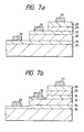
- Fig. 7a shows a sectional structure of an ideal HBT.
- n+-GaAs (sub-collector) layer 34 there are sequentially formed n+-GaAs (sub-collector) layer 34, n-GaAs (collector) layer 32, p+-GaAs (base) layer 31, n-Al x Ga l-x As (emitter) layer 29 and n+-GaAs (cap) layer 28 on a semi-insulated GaAs substrate 35.
- the lithography and etching process are repeated for forming an emitter area, base electrode contact portion and a collector electrode contact portion, and finally an emitter electrode 27, base electrode 30 and collector electrode 33 are formed by a lift-off method.
- etching is not stopped accurately on the surfaces of the p+-GaAs (base) layer 31 and n+-GaAs (sub-collector) layer 34, the over-etching is conducted as shown in Fig. 7b.
- the p+-GaAs (base) layer 31 is made thinner which increases a base resistance.
- the maximum oscillating frequency f max of the HBT is proportional to the inverse number of the square root of the base resistance R b as shown in the equation (8).
- f max f t 8 ⁇ R b C bc wherein f t is a gain cut-off frequency and C bc is a base collector capacity.
- the present invention is applied for the etching of the n-Al x Ga l-x As (emitter) layer 29.
- a wafer is obtained by forming each layer of HBT using a MBE equipment with an ultra-high vacuum, and then forming a resist mask on an emitter area by lithography.
- the wafer is placed in an etching chamber as shown in Fig. 2.
- the usual RIE is conducted using an etching gas of CCl2F2. In this etching, only the n+-GaAs (cap) layer 28 is etched, and thus the surface of n-Al x Ga l-x As (emitter) layer 29 is exposed.
- the RIE is conducted using an etching gas of CCl4 and a source gas of (TMGa + AsH3), and a low pressure mercury lamp as a light source of the photo-CVD.
- a source gas of (TMGa + AsH3) a source gas of (TMGa + AsH3)
- a low pressure mercury lamp as a light source of the photo-CVD.
- the wafer is taken-out and formed with a resist mask so as to expose a sub-collector area, after which the p+-GaAs (base) layer 31 and the n-GaAs (collector) layer 32 are etched by the RIE using the etching gas of CCl4. Finally, an emitter electrode 27, base electrode 30 and collector electrode 33 are formed by a lift-off method.
- the maximum oscillating frequency f max of the HBT in this Example is made higher (approximately 60 GHz) as compared with the conventional manner (30-50 GHz). Further, the scattering thereof is almost eliminated resulting in the improved characteristics.
- the etching is stopped at the depth of the desired composition.
- the sample used in this Example is shown in Fig. 8a.
- the sample is obtained by forming an Al x Ga l-x As layer 36 having a graded composition to a thickness of 100nm on a semi-insulated substrate 35 by a MBE method.
- the composition (x) is set to be 0.3 at the surface and 0.0 at the interface to coincide with the substrate, that is, GaAs.
- the etching is conducted while irradiating a laser beam with a wavelength of 773 nm. This wavelength corresponds to the band gap energy of the composition (x) of the Al x Ga l-x As in the equation (7) and at the temperature of 300K.
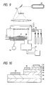
- etching equipment used in this Example is shown in Fig. 9.
- the characteristics of this etching equipment are as follows:
- the light source for inducing the photo-CVD reaction there is used a solid-state tunable laser 37 having a laser crystal of Alexandrite (BeAl2O4) and a pumping of a mercury arc lamp. Further, there is used a RF electrode 38 having a heater and a watercooling mechanism. To stop the etching at the specified composition, it is required to irradiate the light having a wavelength accurately corresponding to the band gap energy at the composition. Also, since the band gap energy is changed depending to the temperature, it also becomes important to keep the substrate temperature at constant.
- a solid-state tunable laser 37 having a laser crystal of Alexandrite (BeAl2O4) and a pumping of a mercury arc lamp.
- a RF electrode 38 having a heater and a watercooling mechanism.
- the sample 11 is placed in the etching chamber 9, and the etching is conducted in the same manner as in Example 1. Namely, an etching gas (CCl4) and a source gas of GaAs (TMGa+AsH3) are introduced in this order into the etching chamber 9, after which the irradiation of the laser beam from the solid-state tunable laser 37 is started. Finally, the gases in the etching chamber are discharged. The sample is kept at a temperature of 300 ⁇ K.
- the GaAs film on the etched surface is very thin, which can be simply removed by dry etching or wet etching.
- the source gas for CVD may be added with a TMAI(Al(CH3)3:trimethyle-aluminum) as a source gas of aluminum.
- the partial pressures of the TMGa and TMAI are respectively adjusted such that the composition (x) of the Al x Ga l-x As layer formed by the photo-CVD reaction becomes 0.15.
- the photo-CVD reaction has been used in this Example; however, as shown in the next Example 7, by using the etching equipment improving that as shown in Fig. 4 wherein the Ar ion laser 16 is replaced into the solid-state tunable laser 37, and the substrate holder 16 includes a heater and cooling mechanism, the present invention utilizing the photo-oxidation reaction can be applicable.
- Example 6 is further developed and the present invention is applicable for fabrication of a HBT having a graded composition base layer.
- Fig. 10 shows a structure of the HBT having the graded composition base layer.
- an electric field is generated in a base region, which accelerates an electron, that is, shortens the base traveling time of the electron thus improving the RF characteristic.
- Example 6 As mentioned in the last of Example 6, there is used the etching equipment improving that as shown in Fig. 4.
- a resist mask is formed on an emitter area by lithography.
- a n+-GaAs (cap) layer 28 is selectively etched by an usual RIE equipment using an etching gas of CCl2F2 so as to expose the surface of a n-Al x Ga l-x As (emitter) layer 29.
- the wafer is set in an etching chamber 9 of the etching equipment improving that as shown in Fig. 4, and the selective etching of the present invention utilizing the photo-oxidation reaction is conducted.
- the wafer is taken out of the etching chamber 9 and is then formed with a resist mask such that a sub-collector region is exposed.
- the p+-Al x Ga l-x As (graded composition base) layer 39 and a u-GaAs (collector) layer 40 are respectively etched by the RIE using the etching gas of CCl4.
- an emitter electrode 27, base electrode 30 and collector electrode 33 are formed by a known lithography method.
- the HBT having the graded composition formed in this Example has the maximum oscillating frequency of approximately 80 GHz, with little scattering of thereof.
- the present invention is applicable as it is.
- the present invention is applied for checking the thickness of Al x Ga l-x As crystal growth film.
- the most simple method for measuring the thickness of the crystal growth film is to partially etch the crystal growth film and measure the height of the step by a stylus thickness meter. A plurality of points on the wafer can be measured for a short time by this method. Consequently, this method is suitable for checking the thickness distribution. Since the etching of only the GaAs layer is possible by the conventional dry etching, the thickness of the GaAs film formed on the Al x Ga l-x As is measured by the above method. In this Example, the Al x Ga l-x As film can be selectively etched, which makes it possible to measure the thickness distribution of the Al x Ga l-x As film formed on the GaAs wafer, in contrast with the conventional one.
- Figs. 11a to 11c show a method for measuring the thickness distribution according to this Example.
- a resist mask 41 is formed on a sample obtained by growing an Al x Ga l-x As film 42 on a GaAs wafer 43.
- Fig. 1b only the exposed portion of the Al x Ga l-x As film 42 is etched.
- the resist mask 41 is removed for revealing the step as shown in Fig. 11.
- the step height is measured by the stylus thickness meter, resulting in the obtained thickness distribution.
- the present invention utilizing the photo-CVD reaction is applied for the fabrication process of HIGFET (Heterostructure Insulated Gate Field Effect Transistor).
- HIGFET Heterostructure Insulated Gate Field Effect Transistor
- Fig. 12 shows a sectional structure of the HIGFET having such a feature that a Schottky junction formed between a W/WSi gate 44 and a u-Al 0.3 Ga 0.7 As 46 artificially serves as an insulating film.
- the fabricating procedure of the HIGFET is as follows: a GaAs (buffer) layer 54, p-GaAs layer 53, n-GaAs (channel) layer 47 and u-Al 0.3 Ga 0.7 As 46 are formed on a semi-insulated GaAs substrate 35 by epitaxial growth.
- the film of each layer and the impurity concentration are shown in Table 2. Table 2 No.
- the mesa-etching is conducted on the way of the p-GaAs layer 53. Thereat, there is formed the W/WSi gate 44. Subsequently, there are formed a SiO2 pattern 52 and a gate electrode side wall SiO2 film 51. This is shown in Fig. 12b. After masking of the SiO2 pattern 52 and the gate electrode side wall SiO2 film 51, the exposed portion of the u-Al 0.3 Ga 0.7 As layer 46 is etched. In this Example, the present invention is applied for the etching of the u-Al 0.3 Ga 0.7 As layer 46. After that, using MOCVD, a n+-GaAs layer 50 is selectively grown, and the source electrode/drain electrode 49 are respectively formed by a known lift-off method, to thus obtain the HIGFET.
- the etching is not stopped at the surface of the GaAs (channel) layer under the u-Al 0.3 Ga 0.7 As layer 46, thus causing the over-etching.
- the over-etching is essential to perfectly remove the u-Al 0.3 Ga 0.7 As layer 46.
- the n-GaAs layer (channel) layer 47 is made thinner, and thus the source resistance and drain resistance are increased, which deteriorates the characteristic of the HIGFET.
- the present invention only the u-Al 0.3 Ga 0.7 As layer 46 is etched, and therefore, there little occurs the over-etching thereby eliminating a fear of causing such a trouble.
- the wafer after completing the processes as shown in Fig. 12b is placed in an etching chamber 9 of the etching equipment as shown in Fig. 9.
- the oscillating wavelength of the solid-state tunable laser 37 is adjusted to be 800 nm.
- the light having such a wavelength is not absorbed by the u-Al 0.3 Ga 0.7 As layer 46 but by only the n-GaAs layer (channel) layer 47.
- the etching is conducted in the same procedure as in Example 1, except that in completing the selective etching, the laser beam irradiation from the solid-state tunable laser 37 and the supply of TMGa and AsH3 are previously stopped and the usual RIE is conducted for 5 min.
- the thin GaAs film formed on the whole surface, for example, on the SiO2 pattern 52 is removed by discharge in a vapor phase. Consequently, as shown in Fig. 12c, only the u-Al 0.3 Ga 0.7 As layer 46 is selectively etched.
- a n+-GaAs layer 50 is re-grown by the MOCVD using a source gas of (TMGa+AsH3) and a doping gas of Si2H6, and finally the source electrode/drain electrode 49 are respectively formed by the lift-off method, to thus obtain the HIFET.
- the source resistance is 0.5 ⁇ mm, which is significantly improved as compared with the conventional value of 0.7 ⁇ mm.
- the present invention is applied for a recessed gate HEMT (High Electron Mobility Transistor).
- Fig. 13 shows a sectional structure of the HEMT.
- the thickness of each layer and the impurity concentration are shown in Table 3.
- the structure of the usual HEMT is shown in Fig.13a.
- the characteristic of the HEMT device is significantly affected by the resistance of the gap between the gate electrode 45 and the n+-GaAs (cap) layer 28.
- the gap is required to secure the break-down resistance between the gate electrode 45 and the n+-GaAs (cap) layer 28. While the dimension is contracted in the lateral direction in Fig. 13a, the distance of the above gap is usually 100-300nm, and the depth from the gate electrode 45 to the channel layer is several ten nm.
- the source resistance is dependent on the concentration of the carriers remaining on the channel layer under the above gap portion 63.
- the n-Al 0.15 Ga 0.85 As (carrier supply) layer 59 is thinner, which exert a large effect on the device having a low threshold voltage.
- the recessed gate HEMT as shown in Fig. 13b provides the u-GaAs (cover) layer 57 for increasing the carrier concentration. Since the u-GaAs (cover) layer 57 lowers the conduction band energy of the whole heterostructure under the u-GaAs (cover) layer 57, the concentration of the carriers remaining in the u-In x Ga l-x As (channel) layer 61 is increased, the resistance of the above gap portion is reduced, and the source resistance is reduced. As a result, a mutual conductance gm is enhanced, which makes it possible to improve the characteristics of the device such as a cut-off frequency f t , maximum oscillating frequency f max and noise factor NF.
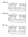
- the gate portion of the recessed gate HEMT is usually fabricated in the procedure as shown in Figs. 14a to 14c.
- a SiO2 film 65 is wet etched using a resist pattern 64 for forming the gate as a mask, and the n+-GaAs film 28 being a cap layer is selectively etched by the RIE.
- the u-Al 0.3 Ga 0.7 As layer 56 serves to stop the etching.
- the over-etching is conducted, and consequently the etching is progressed in the lateral direction.
- Fig. 14a there is formed the above gap portion between the n+-GaAs layer 28 and the gate electrode.
- the u-Al 0.3 Ga 0.7 As layer 56 is selectively etched.
- the above state is shown in Fig. 14b.
- the selective etching is seemed to be very important. The reason for this is that the u-GaAs (cover) layer 57 is over-etched to be thinned, and the concentration of the carriers remaining in the channel is reduced, which increases the resistance of the above gap portion.
- the resist pattern 64 for forming the gate the u-GaAs (cover) layer 57 is selectively etched by the RIE, to thus obtain the recessed gate portion.
- the present invention has been applied for etching the u-Al 0.3 Ga 0.7 As (etching stop) layer 56.
- the etching is conducted using the etching equipment as shown in Fig. 9.
- the wavelength of the solid-state tunable laser is adjusted to be 800 nm.
- the wafer completing the wet etching of the SiO2 film 65 is set in the etching chamber 9, and the n+-GaAs (cap) layer 28 is selectively etched by the RIE using the etching gas of CCl2F2.
- the etchings are conducted in the different manners: the n+-GaAs (cap) layer 28, RIE; u-Al 0.3 Ga 0.7 As (cover) layer 56, wet etching; and u-GaAs (cover) layer 57, RIE.
- the recessed gate structure can be fabricated in one etching equipment by changing the gases.
- the present invention it is possible to selectively etch the indirect transition material to the direct transition material among the materials having the different types of band gap energies. Also, among the direct semiconductors, the semiconductor having a wide band gap energy can be selectively etched.
Landscapes
- Drying Of Semiconductors (AREA)
- Bipolar Transistors (AREA)
- Junction Field-Effect Transistors (AREA)
Applications Claiming Priority (2)
| Application Number | Priority Date | Filing Date | Title |
|---|---|---|---|
| JP3239242A JPH0582490A (ja) | 1991-09-19 | 1991-09-19 | 選択エツチングの方法、装置 |
| JP239242/91 | 1991-09-19 |
Publications (2)
| Publication Number | Publication Date |
|---|---|
| EP0533497A2 true EP0533497A2 (fr) | 1993-03-24 |
| EP0533497A3 EP0533497A3 (en) | 1993-06-30 |
Family
ID=17041856
Family Applications (1)
| Application Number | Title | Priority Date | Filing Date |
|---|---|---|---|
| EP19920308553 Withdrawn EP0533497A3 (en) | 1991-09-19 | 1992-09-18 | Dry etching method |
Country Status (3)
| Country | Link |
|---|---|
| US (1) | US5401357A (fr) |
| EP (1) | EP0533497A3 (fr) |
| JP (1) | JPH0582490A (fr) |
Cited By (1)
| Publication number | Priority date | Publication date | Assignee | Title |
|---|---|---|---|---|
| EP0892441A3 (fr) * | 1997-06-11 | 1999-08-11 | Nec Corporation | Transistor à effet de champ avec grille enfoncée et méthode de fabrication |
Families Citing this family (9)
| Publication number | Priority date | Publication date | Assignee | Title |
|---|---|---|---|---|
| US5859447A (en) * | 1997-05-09 | 1999-01-12 | Yang; Edward S. | Heterojunction bipolar transistor having heterostructure ballasting emitter |
| US6569775B1 (en) | 1999-03-30 | 2003-05-27 | Applied Materials, Inc. | Method for enhancing plasma processing performance |
| JP3644863B2 (ja) * | 2000-01-24 | 2005-05-11 | 沖電気工業株式会社 | 膜厚分布測定方法 |
| CN101472669A (zh) * | 2006-06-14 | 2009-07-01 | 艾尔科泰克技术公司 | 用于处理和/或提高物质干燥度的方法和设备 |
| JP2008010461A (ja) * | 2006-06-27 | 2008-01-17 | Sharp Corp | ヘテロ接合電界効果型トランジスタおよびヘテロ接合電界効果型トランジスタの製造方法 |
| EP2426702A4 (fr) * | 2009-05-01 | 2014-03-26 | Univ Tokyo | Procede de depôt de semi-conducteur a compose chimique et dispositif associe |
| KR101867999B1 (ko) * | 2011-10-31 | 2018-06-18 | 삼성전자주식회사 | Iii-v족 물질층을 형성하는 방법, iii-v족 물질층을 포함하는 반도체 소자 및 그 제조방법 |
| KR101805634B1 (ko) * | 2011-11-15 | 2017-12-08 | 삼성전자 주식회사 | Ⅲ-ⅴ족 배리어를 포함하는 반도체 소자 및 그 제조방법 |
| JP5920255B2 (ja) * | 2013-03-18 | 2016-05-18 | 株式会社デンソー | 半導体装置の製造方法およびそれに用いられるドライエッチング装置 |
Family Cites Families (6)
| Publication number | Priority date | Publication date | Assignee | Title |
|---|---|---|---|---|
| JPH0642456B2 (ja) * | 1984-11-21 | 1994-06-01 | 株式会社日立製作所 | 表面光処理方法 |
| JPS61278146A (ja) * | 1985-06-03 | 1986-12-09 | Toshiba Corp | 光処理方法 |
| US4648938A (en) * | 1985-10-11 | 1987-03-10 | The United States Of America As Represented By The United States Department Of Energy | Composition/bandgap selective dry photochemical etching of semiconductor materials |
| US4880493A (en) * | 1988-06-16 | 1989-11-14 | The United States Of America As Represented By The United States Department Of Energy | Electronic-carrier-controlled photochemical etching process in semiconductor device fabrication |
| EP0374036B1 (fr) * | 1988-12-13 | 1994-10-12 | Fujitsu Limited | Procédé pour la fabrication de dispositifs à semi-conducteur utilisant la gravure sélective assistée par de l'U.V. de multicouches |
| US5092957A (en) * | 1989-11-24 | 1992-03-03 | The United States Of America As Represented By The United States Department Of Energy | Carrier-lifetime-controlled selective etching process for semiconductors using photochemical etching |
-
1991
- 1991-09-19 JP JP3239242A patent/JPH0582490A/ja active Pending
-
1992
- 1992-09-01 US US07/937,781 patent/US5401357A/en not_active Expired - Fee Related
- 1992-09-18 EP EP19920308553 patent/EP0533497A3/en not_active Withdrawn
Cited By (3)
| Publication number | Priority date | Publication date | Assignee | Title |
|---|---|---|---|---|
| EP0892441A3 (fr) * | 1997-06-11 | 1999-08-11 | Nec Corporation | Transistor à effet de champ avec grille enfoncée et méthode de fabrication |
| US6172384B1 (en) | 1997-06-11 | 2001-01-09 | Nec Corporation | Field effect transistor and a method for manufacturing a same |
| US6417035B2 (en) | 1997-06-11 | 2002-07-09 | Nec Corporation | Method for manufacturing a field effect transistor |
Also Published As
| Publication number | Publication date |
|---|---|
| EP0533497A3 (en) | 1993-06-30 |
| JPH0582490A (ja) | 1993-04-02 |
| US5401357A (en) | 1995-03-28 |
Similar Documents
| Publication | Publication Date | Title |
|---|---|---|
| US4477311A (en) | Process and apparatus for fabricating a semiconductor device | |
| US5701019A (en) | Semiconductor device having first and second stacked semiconductor layers, with electrical contact to the first semiconductor layer | |
| EP0964453A2 (fr) | Dispositif comprenant une couche d'oxyde sur un corps semi-conducteur à base de GaAs et sa methode de fabrication | |
| US9059081B2 (en) | Selectively doped semi-conductors and methods of making the same | |
| US5401357A (en) | Dry etching method | |
| JPH11126758A (ja) | 半導体素子製造方法 | |
| US6764883B1 (en) | Amorphous and polycrystalline silicon nanolaminate | |
| EP0374036B1 (fr) | Procédé pour la fabrication de dispositifs à semi-conducteur utilisant la gravure sélective assistée par de l'U.V. de multicouches | |
| EP0208851A1 (fr) | Fabrication d'un dispositif semi-conducteur au moyen d'épitaxie par faisceau moléculaire | |
| JP3792003B2 (ja) | 半導体発光素子 | |
| Nishizava et al. | Latest molecular layer epitaxy technology | |
| JP3236228B2 (ja) | 半導体デバイス及びその製造方法 | |
| JP3211227B2 (ja) | GaAs層の表面安定化方法、GaAs半導体装置の製造方法および半導体層の形成方法 | |
| JPH07263383A (ja) | エッチング方法および半導体装置の製造方法 | |
| JPH1032176A (ja) | エッチング方法および半導体装置の製造方法 | |
| JP3541324B2 (ja) | 半導体装置の製造方法 | |
| JPH08340105A (ja) | 半導体装置およびその製造方法 | |
| JP2803555B2 (ja) | 極微細トンネル障壁の作製方法 | |
| JP3272531B2 (ja) | 化合物半導体装置の製造方法 | |
| Baba et al. | MBE regrowth with hydrogen cleaning and its application for the fabrication of surface tunnel transistors | |
| JPH09199452A (ja) | エッチング方法および半導体装置の製造方法 | |
| Stockman et al. | Hydrogen in III-V device structures | |
| CN117638648A (zh) | 一种掺铁磷化铟半绝缘外延层及掩埋异质结构的制作方法 | |
| Habibi et al. | Dry sequential process of photochemical etching and surface passivation of In0. 52Al0. 48As using HBr and H2S | |
| JPH0757619A (ja) | 電子放出素子 |
Legal Events
| Date | Code | Title | Description |
|---|---|---|---|
| PUAI | Public reference made under article 153(3) epc to a published international application that has entered the european phase |
Free format text: ORIGINAL CODE: 0009012 |
|
| 17P | Request for examination filed |
Effective date: 19921007 |
|
| AK | Designated contracting states |
Kind code of ref document: A2 Designated state(s): DE GB |
|
| PUAL | Search report despatched |
Free format text: ORIGINAL CODE: 0009013 |
|
| AK | Designated contracting states |
Kind code of ref document: A3 Designated state(s): DE GB |
|
| 17Q | First examination report despatched |
Effective date: 19931202 |
|
| 18D | Application deemed to be withdrawn |
Effective date: 19970703 |