EP0534433A2 - Optisches Regenerator-Relaissystem - Google Patents
Optisches Regenerator-Relaissystem Download PDFInfo
- Publication number
- EP0534433A2 EP0534433A2 EP92116368A EP92116368A EP0534433A2 EP 0534433 A2 EP0534433 A2 EP 0534433A2 EP 92116368 A EP92116368 A EP 92116368A EP 92116368 A EP92116368 A EP 92116368A EP 0534433 A2 EP0534433 A2 EP 0534433A2
- Authority
- EP
- European Patent Office
- Prior art keywords
- optical
- amplifier
- signal
- output signal
- circuit
- Prior art date
- Legal status (The legal status is an assumption and is not a legal conclusion. Google has not performed a legal analysis and makes no representation as to the accuracy of the status listed.)
- Granted
Links
Images


Classifications
-
- H—ELECTRICITY
- H04—ELECTRIC COMMUNICATION TECHNIQUE
- H04B—TRANSMISSION
- H04B10/00—Transmission systems employing electromagnetic waves other than radio-waves, e.g. infrared, visible or ultraviolet light, or employing corpuscular radiation, e.g. quantum communication
- H04B10/29—Repeaters
- H04B10/291—Repeaters in which processing or amplification is carried out without conversion of the main signal from optical form
- H04B10/299—Signal waveform processing, e.g. reshaping or retiming
-
- H—ELECTRICITY
- H04—ELECTRIC COMMUNICATION TECHNIQUE
- H04L—TRANSMISSION OF DIGITAL INFORMATION, e.g. TELEGRAPHIC COMMUNICATION
- H04L7/00—Arrangements for synchronising receiver with transmitter
- H04L7/02—Speed or phase control by the received code signals, the signals containing no special synchronisation information
- H04L7/027—Speed or phase control by the received code signals, the signals containing no special synchronisation information extracting the synchronising or clock signal from the received signal spectrum, e.g. by using a resonant or bandpass circuit
Definitions
- This invention relates to an optical regenerative-repeater, and more particularly to, an optical regenerative-repeater for high speed optical communication.
- a superhigh speed optical transmission system using high-speed optical devices and single mode optical fibers has been proposed to realize a large capacity transmission and a long distance transmission.
- an optical transmission system is required to operate with high speed and to be stable in order to realize a wide-band communication in which various information of image, data and voice are transferred. That is, in such a wide-band communication network, a trank transmission system of time-division multiplexing-transmission type has a capacity of multigigabit-per-second, so that an optical transmitter and an optical receiver used for the system is required to operate with high speed and to operate in wide-band.
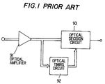
- a conventional optical regenerative-repeater includes an optical amplifier for reshaping an optical input signal by amplification, an optical timing circuit connected to the optical amplifier for extracting an optical timing signal, and an optical decision circuit connected to the optical amplifier and the optical timing circuit, respectively.
- the optical amplifier, the optical timing circuit and the optical decision circuit are connected by optical fibers each other, so that the optical regenerative-repeater system full operates only by processing optical signals.
- the optical signal when an input optical signal is supplied to the optical amplifier, the optical signal is amplified and supplied to the optical timing circuit and to the optical decision circuit, respectively.
- the optical signal is regenerated by the optical decision circuit in accordance with an optical timing signal supplied from the timing circuit.
- optical timing signal supplied from the optical timing circuit is unstable due to practical properties of optical devices and stability thereof, so that timing jitter occurs in the optical timing signal and the jitter is accumulated in an output optical signal from optical repeater.
- an optical regenerative-repeater system includes: an input optical amplifier for amplifying an input optical signal; an optical branch device for branching an output signal of the optical amplifier; means for converting an optical signal supplied from the optical branch device to an electric signal; means for generating a timing signal in accordance with the electric signal supplied from the converting means; an optical latch circuit for latching an optical main signal supplied from the optical branch device in accordance with the timing signal; and an output optical amplifier for amplifying an output signal of the optical latch circuit to provide an output signal of the system.
- Fig. 1 shows a conventional optical regenerative-repeater system which includes an optical amplifier 91 for reshaping an input signal by amplification, an optical timing circuit 92 connected at input to output of the optical amplifier 91 for generating an optical timing signal, and an optical decision circuit 93 connected at data input to output of the optical amplifier 91 and at timing signal input to output of the optical timing circuit 92, respectively.
- the optical amplifier 91, the optical timing circuit 92 and the optical decision circuit 93 are connected by optical fibers each other, so that the system wholly operates optically without conversion between optical and electrical signals.
- the signal when an input optical signal is supplied to the optical amplifier 91, the signal is amplified and supplied to the optical timing circuit 92 and to the optical decision circuit 93, respectively.
- the optical signal is regenerated by the decision circuit 93 in accordance with a timing signal supplied from the optical timing circuit 92.
- optical timing signal supplied from the optical timing circuit is unstable due to practical properties of optical devices and stability thereof, so that timing jitter occurs in the optical timing signal and the jitter is accumulated in an optical output signal from the repeater.
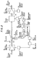
- Fig. 2 shows an optical regenerative-repeater system of a first preferred embodiment according to the invention.
- the optical regenerative-repeater system includes an optical amplifier 12 connected to an input optical fiber 11, a current supply circuit 13 connected to the optical amplifier 12 for supplying injection current to the optical amplifier 12, an isolator 14 connected to the optical amplifier 11, an optical branch device 15 connected to the isolator 14 for branching a signal, a photo detector 16 connected to the optical branch device 15, an optical latch circuit 17 connected to the optical branch device 15, a wide-band amplifier 18 connected to the photo detector 16, a differentiating circuit 19 connected to the wide-band amplifier 18, a full-wave rectification circuit 20 connected to the differentiating circuit 19, a timing tank 21 connected to the full-wave rectification circuit 20, a narrow-band amplifier 22 connected to the timing tank 21, a current supply circuit 23 connected at an input to the narrow-band amplifier 22 and at an output to the optical latch circuit 17, a peak detector 24 connected at an input to an output of the full-wave rectification circuit 20,
- the narrow-band amplifier 22 is tuned to amplify a timing frequency portion of the supplied signal which is selected in the timing tank 21 to be synchoronous with a data transmission rate of a transmission line, so that output signal levels are quite different between in a transmission mode and in no transmission mode.
- a surface acoustic wave filter may be used as the timing tank 21.
- a specific bandwidth Q is preferably large for a timing characteristic, however, the specific bandwidth Q is sufficient to be about 1000 if thermal fluetuation, practicability and the like is considered.
- optical latch circuit 17 The detailed theory of the optical latch circuit 17 is described in a technical report "Studying of Time-division Multiplex Optical Switching System using a bistable LD" by Suzuki et al., Electronics Information and Communication Society, SE 84-62, October, 1987.
- the input signal is amplified optically by the optical amplifier 12 in accordance with a gain determined by amount of injection current supplied from the current supply circuit 13.
- the optical amplifier 12 has a bandwidth of zero to over nine tera Hz which may not be realized by an optical receiver using APD (avalanche photo diode). That is, substantially, there is no limitation about bandwidth to the amplifier 12.
- APD avalanche photo diode
- an output signal of the optical amplifier 12 is supplied via the isolator 14, for removing the infulence of reflection to the amplifier 12 to the optical branch device 15, by which the signal is branched to two signals.
- An optical narrow-band filter (not shown) may be provided between the optical amplifier 12 and the isolator 14 in order to avoid reducing of S/N ratio by spontaneous emission optical noise supplied from the amplifier 12.
- the bandwidth of the filter is determined to be around 1 nm.
- the output signals of the optical branch device 15 are supplied to the optical latch circuit 17 and the photo detector 16, respectively.
- the signal supplied to the photo detector 16 is converted to an electric signal, and the electric signal is supplied to the wide-band amplifier 18.
- the signal is amplified to be a predetermined level by the wide-band amplifier 18.
- a transmission code is NRZ (non return to zero) code
- no timing bright line spectrum is included in the output signal of the amplifier 18. Therefore, a timing bright line spectrum is generated by the differentiating circuit 19 and the full-wave rectification circuit 20, and the timing bright line spectrum is supplied to the timing tank 21.
- the timing tank 21 supplies a timing signal having a frequency synchronized with a rate of the transmission data to the narrow-band amplifier 22.
- the signal is amplified to be a sufficient level by the amplifier 22, and the amplified signal is supplied to the current supply circuit 23 which is for driving the optical latch circuit 17.
- the optical latch circuit 17 discriminates an optical data supplied from the optical branch device 15 without any conversion to electric signal in accordance with timing of current supplied from the current supply circuit 23.
- An output signal of the optical latch circuit 17 is supplied to the optical amplifier 27, so that an optical output signal is supplied from the optical amplifier 27 to the output optical fiber 29 in accordance with injection current supplied from the current supply circuit 28.
- an output signal of the full-wave rectification circuit 20 is supplied to the peak detector 24, a peak value of the signal is detected by the detector 24.
- the signal is compared with a predetermined reference voltage, and a control signal having a voltage level determined in accordance with the result of the comparison is supplied to the current supply circuit 13.
- the current supply circuit 13 supplies a current signal of amount corresponding to the output level of the DC amplifier 25 to the optical amplifier 12, so that amplifying gain of the amplifier 12 is controlled by the current signal. Therefore, the output level is a sufficient level for a transmission signal.
- the output level of the optical amplifier 12 is stabilized at a predetermined level, that is, an AGC (automatic gain control ) is carried out by the operation.
- jitter in a timing signal to be supplied to the optical latch circuit 17 is reduced, because the timing signal is generated by the electric system (16 and 18 to 23), while optical transmission data is subject to no conversion to electric signal, so that jitter is not accumulated in the output signal. Therefore, characteristics of the optical regenerative-repeater system is improved.
- a level of the output signal is stable even if an input signal level changes, because transmission gain of the input signal is controlled at the optical amplifier 12 in accordance with a peak value of the input signal detected by the peak detector 24 using an output signal of the full-wave rectification circuit 20.
- Fig. 3 shows an optical regenerative-repeater system of a second preferred embodiment according to the invention.
- the same structure and the same operation as the first preferred embodiment shown in Fig. 2 will be omitted.
- the optical regenerative-repeater system includes a current supply circuit 231 instead of the current supply circuit 23 of the first preferred embodiment, and a peak detector 232 connected to the narrow-band amplifier 22, and a DC amplifier 233 connected at an input to the peak detector 232 and at an output to the current supply circuit 231.
- the system is prohibited from supplying useless noise, when no data signal is supplied to the system and noise signal is supplied to the system.
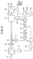
- Fig. 4 shows an optical regenerative-repeater system of a third preferred embodiment according to the invention.
- the optical regenerative-repeater system is controlled more precisely in prohibiting the supply of useless noise than the second preferred embodiment.
- the same structure and the same operation as the second preferred embodiment shown in Fig. 3 will be omitted.
- the optical regenerative-repeater system includes a current supply circuit 38 instead of the current supply circuit 28 of the first preferred embodiment shown in Fig. 3.
- the current supply circuit 38 is connected at an input to the DC amplifier 233.
- an alarm signal is supplied from the DC amplifier 233 to the current supply circuit 38 in addition to the current supply circuit 231, so that no driving current is supplied from the current supply circuit 38 to the optical amplifier 27 at no input signal state. Therefore, the optical amplifier 27 is prohibited from operating.
- Fig. 5 shows an optical regenerative-repeater system of a fourth preferred embodiment according to the invention.
- the same structure and the same operation as the third preferred embodiment shown in Fig. 4 will be omitted.
- the optical latch circuit 17 and the optical amplifier 27 are controlled to be prohibited from supplying a signal in accordance with not only the output signal of the DC amplifier 233 but also with monitoring result of an input signal.
- the optical regenerative-repeater system includes an optical branch device 41 connected at an input to the input optical fiber 11 and at one of outputs to the optical amplifier 12, a photo detector 42 connected to the optical branch device 41, a DC amplifier 43 connected at an input to the photo detector 42, and an AND circuit connected at inputs to the DC amplifiers 43 and 233 and at outputs to the current supply circuits 231 and 38.
- a voltage signal having a level corresponding to an average of the input current is supplied from the photo detector 42 to the DC amplifier 43.
- the supplied voltage is compared with a reference voltage Vref2 corresponding to an input signal voltage at no input signal state. And, when the input voltage is equal to the reference voltage Vref2, an alarm signal, for instance, a TTL level signal is supplied to the AND circuit 44.
- the reference voltage Vref2 is determined so that it can be classified from the minimum mark ratio of the optical input data.
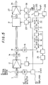
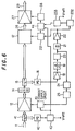
- Fig. 6 shows an optical regenerative-repeater system of a fifth preferred embodiment according to the invention.
- the same structure and the same operation as the fourth preferred embodiment shown in Fig. 5 will be omitted.
- the optical amplifier 12 is controlled to be prohibited from supplying a signal to the isolator 14. That is, the optical regenerative-repeater system includes a current supply circuit 53 instead of the current supply circuit 13 of the fourth preferred embodiment shown in Fig. 5.
- the current supply circuit 53 is connected at inputs to the DC amplifiers 43 and 25 and at an output to the optical amplifier 12.
- the current supply circuit 53 In operation, when an alarm signal is supplied from the DC amplifier 43 to the current supply circuit 53, the current supply circuit 53 is prohibited from supplying a driving current to the optical amplifier 12.
- Fig. 7 shows an optical regenerative-repeater system of a sixth preferred embodiment according to the invention.
- the same structure and the same operation as the fifth preferred embodiment shown in Fig. 6 will be omitted.
- the optical regenerative-repeater system has a function to monitor a trouble location. That is, the optical regenerative-repeater system includes a DC amplifier 64 connected at an input to the peak detector 24, an alarm monitor circuit 65 connected at an input to the output of the DC amplifier 43, an alarm monitor circuit 66 connected at inputs to outputs of the DC amplifier 64 and the alarm monitor circuit 65, an alarm monitor circuit 67 connected at inputs to outputs of the alarm monitor circuit 66 and the DC amplifier 233.
- the alarm monitor circuits 65 to 67 have output terminals 68, 69 and 600 each connected to an external monitor system (not shown).
- a high level signal is supplied from the DC amplifier 43 to the alarm monitor circuit 65, a high level signal is supplied from the alarm monitor circuit 65 to the external monitor system and to the alarm monitor circuit 66.
- Each of the alarm monitor circuits 66 and 67 supplies a high level output signal, when at least one of input signals is a high level signal. That is, when high level signals are supplied from all of the alarm monitor circuits 65 to 67, it is judged that no input signal is supplied to the system (the optical amplifier 12) through the input optical fiber 11.
- high level signals are supplied from only the alarm monitor circuits 66 and 67, it is judged that, though an input signal is supplied to the system, anything unusual occurs at a location of the amplifier or subsequent thereto. And, when high level signal is supplied from only the alarm monitor circuit 67, it is judged that there is anything unusual in the timing generating portion (18 to 22).
- Fig. 8 shows an optical regenerative-repeater system of a seventh preferred embodiment according to the invention.
- the same structure and the same operation as the sixth preferred embodiment shown in Fig. 7 will be omitted.
- the optical regenerative-repeater system includes an optical branch device 71 connected to the optical amplifier 27, a photo detector 72 connected to the optical branch device 71, and a DC amplifier 73 connected at an input to the photo detector 72 and at an output to the current supply circuit 38.
- the signal is converted to an electric signal by the photo detector 72, and the electric signal (voltage signal) is supplied to the DC amplifier 73.
- the DC amplifier 73 supplies a control signal having a level determined in accordance with a level of the voltage signal from the photo detector 72 to the current supply circuit 38.
- the current supply circuit 38 supplies a current signal to the optical amplifier 27 in accordance with the control signal supplied from the DC amplifier 73, so that gain of the optical amplifier 27 is controlled by feed back. Therefore, an output level of the optical regenerative-repeater system can be controlled to be stabilized.
- Fig. 9 shows an optical regenerative-repeater system of an eighth preferred embodiment according to the invention.
- the same structure and the same operation as the seventh preferred embodiment shown in Fig. 8 will be omitted.
- the optical regenerative-repeater system includes a DC amplifier 81 connected at an input to the output of the photo detector 72 and at one of outputs to the current supply circuit 38, and an alarm monitor circuit 83 connected at inputs to the alarm monitor circuit 67 and to the other output of the DC amplifier 81 and at an output to an output terminal 67 which is connected to the external monitor system.
- the signal is compared with a reference voltage Vref4 which corresponds to a predetermined output level of the optical amplifier 27.
- Vref4 a reference voltage which corresponds to a predetermined output level of the optical amplifier 27.
- the DC amplifier 81 supplies a control signal 82 to the current supply circuit 38 to be prohibited from supplying current signal to the optical amplifier 27.
- an alarm signal 85 is supplied from the DC amplifier 81 to the alarm monitor circuit 83.
Landscapes
- Physics & Mathematics (AREA)
- Electromagnetism (AREA)
- Engineering & Computer Science (AREA)
- Computer Networks & Wireless Communication (AREA)
- Signal Processing (AREA)
- Optical Communication System (AREA)
Applications Claiming Priority (2)
| Application Number | Priority Date | Filing Date | Title |
|---|---|---|---|
| JP3273212A JP2661438B2 (ja) | 1991-09-24 | 1991-09-24 | 光再生中継器 |
| JP273212/91 | 1991-09-24 |
Publications (3)
| Publication Number | Publication Date |
|---|---|
| EP0534433A2 true EP0534433A2 (de) | 1993-03-31 |
| EP0534433A3 EP0534433A3 (en) | 1993-10-06 |
| EP0534433B1 EP0534433B1 (de) | 1997-12-17 |
Family
ID=17524665
Family Applications (1)
| Application Number | Title | Priority Date | Filing Date |
|---|---|---|---|
| EP92116368A Expired - Lifetime EP0534433B1 (de) | 1991-09-24 | 1992-09-24 | Optisches Regenerator-Relaissystem |
Country Status (4)
| Country | Link |
|---|---|
| US (1) | US5379143A (de) |
| EP (1) | EP0534433B1 (de) |
| JP (1) | JP2661438B2 (de) |
| DE (1) | DE69223577T2 (de) |
Cited By (8)
| Publication number | Priority date | Publication date | Assignee | Title |
|---|---|---|---|---|
| EP0555063A3 (en) * | 1992-02-03 | 1993-12-08 | Kokusai Denshin Denwa Co Ltd | Optical waveform shaping device |
| US5401957A (en) * | 1992-02-03 | 1995-03-28 | Kokusai Denshin Denwa Kabushiki Kaisha | Optical waveform shaping device for peforming waveform equalization and timing synchronization |
| GB2299474A (en) * | 1995-03-31 | 1996-10-02 | Nec Corp | Optical regenerator |
| US5576876A (en) * | 1994-02-07 | 1996-11-19 | Hitachi, Ltd. | Optical regenerator and an optical transmission system |
| GB2302225A (en) * | 1995-06-13 | 1997-01-08 | France Telecom | Optical regenerator |
| EP0765045A1 (de) * | 1995-09-21 | 1997-03-26 | ALCATEL BELL Naamloze Vennootschap | Optische Verstärkungs-Kombinierungsanordnung und Verfahren zur Aufwärtsrichtungsübertragung unter Verwendung einer solchen Anordnung |
| FR2750552A1 (fr) * | 1996-06-26 | 1998-01-02 | Alcatel Submarcom | Recepteur pour systeme de transmission de signaux numeriques par voie optique |
| EP1172950A3 (de) * | 2000-07-15 | 2003-10-29 | Alcatel | Optischer Empfänger |
Families Citing this family (5)
| Publication number | Priority date | Publication date | Assignee | Title |
|---|---|---|---|---|
| RU2105389C1 (ru) * | 1992-07-06 | 1998-02-20 | Самсунг Электроникс Ко., Лтд. | Полностью оптический регенератор |
| US5392146A (en) * | 1993-01-25 | 1995-02-21 | Motorola, Inc. | Optical rotary control device |
| CA2172873C (en) * | 1996-03-28 | 2002-03-12 | Kim Byron Roberts | Method of determining optical amplifier failures |
| GB2320634A (en) | 1996-12-19 | 1998-06-24 | Northern Telecom Ltd | Optical sampling by using an interferometer to modulate a pulse train |
| GB2320635A (en) | 1996-12-19 | 1998-06-24 | Northern Telecom Ltd | Optical timing detection using an interferometer |
Family Cites Families (4)
| Publication number | Priority date | Publication date | Assignee | Title |
|---|---|---|---|---|
| JPS5555591A (en) * | 1978-10-19 | 1980-04-23 | Kokusai Denshin Denwa Co Ltd <Kdd> | Semiconductor light amplifier |
| JPH03247033A (ja) * | 1990-02-23 | 1991-11-05 | Fujitsu Ltd | 光中継器 |
| JPH0834454B2 (ja) * | 1990-03-01 | 1996-03-29 | 国際電信電話株式会社 | 光中継器の監視方式 |
| JP2658607B2 (ja) * | 1991-01-30 | 1997-09-30 | 日本電気株式会社 | 光再生中継器 |
-
1991
- 1991-09-24 JP JP3273212A patent/JP2661438B2/ja not_active Expired - Fee Related
-
1992
- 1992-09-24 DE DE69223577T patent/DE69223577T2/de not_active Expired - Fee Related
- 1992-09-24 EP EP92116368A patent/EP0534433B1/de not_active Expired - Lifetime
- 1992-09-24 US US07/950,004 patent/US5379143A/en not_active Expired - Fee Related
Cited By (16)
| Publication number | Priority date | Publication date | Assignee | Title |
|---|---|---|---|---|
| US5401957A (en) * | 1992-02-03 | 1995-03-28 | Kokusai Denshin Denwa Kabushiki Kaisha | Optical waveform shaping device for peforming waveform equalization and timing synchronization |
| EP0555063A3 (en) * | 1992-02-03 | 1993-12-08 | Kokusai Denshin Denwa Co Ltd | Optical waveform shaping device |
| US5838475A (en) * | 1994-02-07 | 1998-11-17 | Hitachi, Ltd. | Optical regenerator and an optical transmission system |
| US5576876A (en) * | 1994-02-07 | 1996-11-19 | Hitachi, Ltd. | Optical regenerator and an optical transmission system |
| GB2299474B (en) * | 1995-03-31 | 1999-04-07 | Nec Corp | Optical regenerating circuit |
| US5754325A (en) * | 1995-03-31 | 1998-05-19 | Nec Corporation | Optical regenerating circuit |
| GB2299474A (en) * | 1995-03-31 | 1996-10-02 | Nec Corp | Optical regenerator |
| GB2302225A (en) * | 1995-06-13 | 1997-01-08 | France Telecom | Optical regenerator |
| GB2302225B (en) * | 1995-06-13 | 1999-04-07 | France Telecom | An all-optical device for regenerating an optical signal modulated in an RZ format |
| EP0765045A1 (de) * | 1995-09-21 | 1997-03-26 | ALCATEL BELL Naamloze Vennootschap | Optische Verstärkungs-Kombinierungsanordnung und Verfahren zur Aufwärtsrichtungsübertragung unter Verwendung einer solchen Anordnung |
| US5754319A (en) * | 1995-09-21 | 1998-05-19 | Alcatel N.V. | Optical amplifier combiner arrangement and method for upstream transmission realized thereby |
| AU714781B2 (en) * | 1995-09-21 | 2000-01-13 | Alcatel N.V. | Optical amplifier splitter |
| FR2750552A1 (fr) * | 1996-06-26 | 1998-01-02 | Alcatel Submarcom | Recepteur pour systeme de transmission de signaux numeriques par voie optique |
| EP0817408A1 (de) * | 1996-06-26 | 1998-01-07 | Alcatel Submarine Networks | Empfänger für Übertragungssystem eines optischen Digitalsignals |
| US5854704A (en) * | 1996-06-26 | 1998-12-29 | Alcatel Submarine Networks | Receiver for optical digital transmission system |
| EP1172950A3 (de) * | 2000-07-15 | 2003-10-29 | Alcatel | Optischer Empfänger |
Also Published As
| Publication number | Publication date |
|---|---|
| EP0534433A3 (en) | 1993-10-06 |
| DE69223577T2 (de) | 1998-07-23 |
| EP0534433B1 (de) | 1997-12-17 |
| DE69223577D1 (de) | 1998-01-29 |
| US5379143A (en) | 1995-01-03 |
| JP2661438B2 (ja) | 1997-10-08 |
| JPH0583200A (ja) | 1993-04-02 |
Similar Documents
| Publication | Publication Date | Title |
|---|---|---|
| US4415803A (en) | Optical receiver with improved dynamic range | |
| US6594070B2 (en) | Optical communication system, optical receiver and wavelength converter | |
| US6369926B1 (en) | Multichannel light source wavelength and strength stabilizing apparatus and method thereof | |
| US4369525A (en) | Device for automatic regulation of the output power of a transmitter module in an optical-fiber transmission system | |
| US5703711A (en) | In-line optical amplifier | |
| EP0873605B1 (de) | Überwachungsnachrichtenübertragung von einem faserverstärker | |
| US5379143A (en) | Optical regenerative-repeater system | |
| JP4935422B2 (ja) | 前置増幅器およびそれを用いた光受信装置 | |
| JPH1084323A (ja) | 光通信路によるデジタル信号伝送システム用の受信器 | |
| US5563731A (en) | Monitor control signal receiving apparatus for optical fiber amplifier | |
| CN108768533B (zh) | 一种用于高速远距离传输的光收发一体组件 | |
| US5809049A (en) | Method and apparatus for monitoring the RF drive circuit of a linear laser transmitter | |
| US5023942A (en) | Fault tolerant data transmission network | |
| CN208424372U (zh) | 一种用于高速远距离传输的光收发一体组件 | |
| US6912085B2 (en) | Optical amplifier | |
| EP0930729A2 (de) | Optische spannungenunterdrückende Einrichtung | |
| JPH0468830A (ja) | 光増幅装置の制御方法及び光増幅装置 | |
| JP3802232B2 (ja) | 光受信器 | |
| JP2560881B2 (ja) | 光再生中継器 | |
| JP2658607B2 (ja) | 光再生中継器 | |
| JPH10303820A (ja) | Apdを用いた光受信器 | |
| US20030094967A1 (en) | Signal-off detection circuit and optical receiving device using the same | |
| US7136597B2 (en) | Decision system for modulated electrical signals | |
| JPH02125552A (ja) | 光入力断検出回路 | |
| CA1217818A (en) | Optical modulation/demodulation system |
Legal Events
| Date | Code | Title | Description |
|---|---|---|---|
| PUAI | Public reference made under article 153(3) epc to a published international application that has entered the european phase |
Free format text: ORIGINAL CODE: 0009012 |
|
| AK | Designated contracting states |
Kind code of ref document: A2 Designated state(s): DE FR GB |
|
| PUAL | Search report despatched |
Free format text: ORIGINAL CODE: 0009013 |
|
| AK | Designated contracting states |
Kind code of ref document: A3 Designated state(s): DE FR GB |
|
| 17P | Request for examination filed |
Effective date: 19930817 |
|
| 17Q | First examination report despatched |
Effective date: 19960513 |
|
| GRAG | Despatch of communication of intention to grant |
Free format text: ORIGINAL CODE: EPIDOS AGRA |
|
| GRAG | Despatch of communication of intention to grant |
Free format text: ORIGINAL CODE: EPIDOS AGRA |
|
| GRAG | Despatch of communication of intention to grant |
Free format text: ORIGINAL CODE: EPIDOS AGRA |
|
| GRAH | Despatch of communication of intention to grant a patent |
Free format text: ORIGINAL CODE: EPIDOS IGRA |
|
| GRAH | Despatch of communication of intention to grant a patent |
Free format text: ORIGINAL CODE: EPIDOS IGRA |
|
| GRAA | (expected) grant |
Free format text: ORIGINAL CODE: 0009210 |
|
| AK | Designated contracting states |
Kind code of ref document: B1 Designated state(s): DE FR GB |
|
| REF | Corresponds to: |
Ref document number: 69223577 Country of ref document: DE Date of ref document: 19980129 |
|
| ET | Fr: translation filed | ||
| PLBE | No opposition filed within time limit |
Free format text: ORIGINAL CODE: 0009261 |
|
| 26N | No opposition filed | ||
| REG | Reference to a national code |
Ref country code: GB Ref legal event code: IF02 |
|
| PGFP | Annual fee paid to national office [announced via postgrant information from national office to epo] |
Ref country code: FR Payment date: 20060908 Year of fee payment: 15 |
|
| PGFP | Annual fee paid to national office [announced via postgrant information from national office to epo] |
Ref country code: GB Payment date: 20060920 Year of fee payment: 15 |
|
| PGFP | Annual fee paid to national office [announced via postgrant information from national office to epo] |
Ref country code: DE Payment date: 20060922 Year of fee payment: 15 |
|
| GBPC | Gb: european patent ceased through non-payment of renewal fee |
Effective date: 20070924 |
|
| PG25 | Lapsed in a contracting state [announced via postgrant information from national office to epo] |
Ref country code: DE Free format text: LAPSE BECAUSE OF NON-PAYMENT OF DUE FEES Effective date: 20080401 |
|
| REG | Reference to a national code |
Ref country code: FR Ref legal event code: ST Effective date: 20080531 |
|
| PG25 | Lapsed in a contracting state [announced via postgrant information from national office to epo] |
Ref country code: FR Free format text: LAPSE BECAUSE OF NON-PAYMENT OF DUE FEES Effective date: 20071001 |
|
| PG25 | Lapsed in a contracting state [announced via postgrant information from national office to epo] |
Ref country code: GB Free format text: LAPSE BECAUSE OF NON-PAYMENT OF DUE FEES Effective date: 20070924 |