EP0534885A2 - Détection automatique de vitesse pour modems à duplex intégrale - Google Patents
Détection automatique de vitesse pour modems à duplex intégrale Download PDFInfo
- Publication number
- EP0534885A2 EP0534885A2 EP92480118A EP92480118A EP0534885A2 EP 0534885 A2 EP0534885 A2 EP 0534885A2 EP 92480118 A EP92480118 A EP 92480118A EP 92480118 A EP92480118 A EP 92480118A EP 0534885 A2 EP0534885 A2 EP 0534885A2
- Authority
- EP
- European Patent Office
- Prior art keywords
- sequence
- samples
- sum
- complex
- sampling
- Prior art date
- Legal status (The legal status is an assumption and is not a legal conclusion. Google has not performed a legal analysis and makes no representation as to the accuracy of the status listed.)
- Granted
Links
Images


Classifications
-
- H—ELECTRICITY
- H04—ELECTRIC COMMUNICATION TECHNIQUE
- H04L—TRANSMISSION OF DIGITAL INFORMATION, e.g. TELEGRAPHIC COMMUNICATION
- H04L27/00—Modulated-carrier systems
- H04L27/0012—Modulated-carrier systems arrangements for identifying the type of modulation
Definitions
- This invention relates generally to modems, data sets, line adapters and the like where analog modulated waveforms are to be transmitted from a sender to a receiver. More particularly, it relates specifically to automode sensing of modem speeds in accordance with the recommended CCITT modem identification signal sequence called "S1".
- Automode sensing is employed in modems built according to the CCITT V.22 and V.22bis standards to enable the modems to sense and properly distinguish between the V.22, 1200bps modems and the V.22bis which may be 1200 or 2400 bps modems.
- the distinction is based upon sending and receiving during the start-up phase of a short, modulated signal sequence having a standard pattern called the "S1" sequence.
- the S1 sequence when received and recognized by an answering V.22bis modem, indicates that the calling mode has V.22bis capabilities i.e., it is capable of sending and receiving at 2400 bit per second.
- the answering modem receiving the S1 sequence acknowledges the reception of an S1 sequence by also sending such a sequence; when such a sequence is properly received and detected by the calling modem, both modems can declare a V.22bis connection to exist and further start-up sequences may be exchanged to achieve full duplex transmission at the common data rate of 2400 bits per second. Failure of either modem in its mutual exchange of S1 sequences leads to an assumption by both that at least one of the modems is a V.22 capable modem, in which case, the start-up sequences proceed to achieve full duplex transmission at the common data rate of 1200 bps.
- an S1 sequence can quickly be recognized by classical symbol detection methods in the receiving modems. Observance of the S1 sequence based upon the detection of alternating signs in the imaginary part of the complex signals x k is the distinctive feature acknowledged in the prior art as recognition of the reception of an S1 sequence. This technique, however, requires careful adjustment of the sampling phase ⁇ and the carrier phase ⁇ , respectively. Such values are normally not conveniently available at startup because the calling modem begins transmission of its S1 sequence abruptly and without a preamble. The receiving or answering modem must then acquire proper sample phase timing ⁇ and carrier phase synchronization ⁇ very quickly if the S1 sequence is to be recognized by the classical symbol detection method.
- the S1 sequence in the CCITT V.22bis modem standard consists of a four phase shift keyed signal having alternating phase shifts of plus or minus 90 degrees transmitted at the modulation rate of 1 divided by T.
- the S1 complex sequence signal is amplitude sampled at twice per modulation interval T to obtain four complex values x k equal to x 2n ⁇ 0, x 2n- 1, x 2n ⁇ 2 and x 2n ⁇ 3, respectively.
- the samples are interleaved with the two even numbered samples being considered together and the two odd numbered samples being considered together, by performing a complex multiplication of the paired samples followed by scalar multiplication between the imaginary part from the complex multiplied samples and the time delayed result of the previous similar complex multiplication where, the time delay is equal to 1 modulation interval T.
- the same operations are conducted for the two odd numbered samples and the result of its scalar multiplication is added with the result of the first scalar multiplication in a summing operation. It has been discovered that when the sign of the resultant sum is negative i.e. where the sum is less than zero continuously for successive sets of samples, that an S1 sequence exists.
- Figure 1 illustrates the four phase shift keyed symbol transmissions base in a polar coordinate diagram illustrating symbols ABC and D.
- Figure 2 illustrates a modulated complex base band S1 sequence as it would be seen over a continuous time on an oscilloscope at a receiver receiving an S1 baseband sequence with an arbitrary phase angle phi.
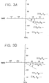
- Figure 3a illustrates the results of sampling an S1 sequence at a receiver to measure instantaneous amplitudes at four sampling times at T/2 intervals relative to an arbitrary clock, ⁇ , and carrier phases ⁇ in the complex number domain to obtain x 2n ⁇ 0, x 2n ⁇ 1, X 2n ⁇ 2, x 2n ⁇ 3 sample sequences.
- Figure 3b illustrates the result of similar sampling in the complex domain by complex baseband sampling known in the art and at a different arbitrary clock phase ⁇ when both Figures 3a and 3b have the same arbitrary carrier phase ⁇ .
- Figure 4 illustrates a preferred embodiment of the circuitry for combining complex samples and calculating the results which lead to detection of an S1 sequence in accordance with the invention.
- Figure 5 illustrates schematically the timing and placement of the complex samples in the real and imaginary domains as utilized in the preferred embodiment of the invention.
- Figure 6 illustrates schematically the complex sampler used to provide the sample stream for use in the preferred embodiment of Figure 4.
- This invention eliminates the prior requirement for synchronization of the carrier phase and sampling phase between sending and receiving modems prior to accurate detection of an S1 identification signal sequence. It has been found that certain mathematical combinations of the complex signal samples lead to a correlation that uniquely identifies an S1 sequence if the signal samples are spaced at the modulation interval, T. It has been found that two sets of T-spaced, "interlaced" (that is time alternated samples as shall appear herein) samples may be used to form sample sets which are processed at each modulation interval to yield imaginary components. The imaginary components are then combined to form a sum or metric which is invariant to either sampling or carrier phase differences. Further filtering of this metric, via appropriate low pass filters combined with counting of sequential occurrences of a sum correlation in comparison with a threshold count for detection, completes the process of S1 signal detection.
- ⁇ and ⁇ may be arbitrary sampling timing phases and carrier phases, respectively.
- u n (1- ⁇ ) u n-1 + ⁇ ( ⁇ cos,n ⁇ cos,n-1 + ⁇ sin,n ⁇ sin,n-1 ), 0 ⁇ 1.
- Either an actual analog hardware filter may be built with the filtering coefficient ⁇ lying in the range of 0 to 1 as shown by equation 6, or a digitally implemented algorithm for filtering may be employed.
- circuitry for performing the algorithm in equations 2 through 5 is shown in Figure 4.
- an incoming analog waveform signal at the receiving point is complex sampled by the sampler 12 which may be simply an analog to digital converters strobed at equal to or more than the Nyquist sampling rate.
- the S1 processing rate selected is, as discussed earlier, twice the modulation rate, or, an interval of T/2.
- consecutive baseband samples are repetitively made and fed into the inputs of the complex multipliers 1 and 2, respectively.
- an incoming signal will be sampled to result in a sample x 2n , a succeeding sample x 2n ⁇ 1, another sample x 2n ⁇ 2 and a fourth sample x 2n ⁇ 3.
- each group of four consecutive samples is handled in the complex multipliers 1 and 2 with the even numbered and the odd numbered samples being taken together.
- the input into the complex multiplier 1 for example comprises a signal x 2n and the next even numbered sample x 2n ⁇ 2 (conjugated) which is displaced in time by T.
- the inputs to the complex multiplier 2 are, likewise, the complex sample x 2n ⁇ 1and x 2n ⁇ 3 (conjugated).
- the even numbered samples and the odd numbered samples at the sampling rate T/2 thus comprise the separate inputs to the different complex multipliers 1 and 2 as shown in Figure 4.
- the complex sample signals have the form as shown above in equation 1.
- the two sets of complex samples represent an arbitrary clock time and its displacement by T/2.
- the output from the complex multipliers 1 and 2 in Figure 4 are the starting point for the calculations for the equations 2 and 3 for calculating the imaginary component of v cos,n and v sin,n , respectively. This fact is indicated in Figure 4 by the numeral 2(Im) (for "imaginary") after the output of the complex multiplier 1 and the numeral 3(Im) after the output of the complex multiplier 2.
- Each of these results is inputted to a time delay circuit 3 or 4, respectively, where a 1 modulation period time delay T is introduced prior to feeding the time delayed calculated imaginary value and the current imaginary value directly to the scalar multiplier 5 as shown in Figure 4, or for the other two complex and conjugate complex samples x 2n ⁇ 1and x 2n ⁇ 3, to the scalar multiplier 6 as shown.
- the results are summed together in the adder 7 whose output is the metric u n as shown by equation 4.
- a decision/comparator circuit 8 receives the input which is the sum.
- the decision circuit compares the value u n to 0 to determine if a negative value is present. If a negative value is present, the "yes" output increments the S1 counter 9 by one and if a non negative result occurs in comparator 8, the "no" output resets counter 9 to zero.
- comparator 10 having an arbitrary threshold value for detection of a valid S1 sequence. It has been found that a threshold of 32 is an appropriate level for comparison. When 32 consecutive occurrences of the metric u n being less than 0 have been counted in counter 9, the comparator 10 will indicate and latch the detection of an S1 sequence, but will otherwise indicate "not S1" as shown.
- AND gate 11 receives the S1 detected input and the u n non negative input to logically indicate the end of the S1 sequence, AND gate 11 is conditioned because negative value u n have been found in sufficient number to indicate the presence of an S1 signal, and then comparator 8 will later indicate the occurrence of a non-negative value for u n .
- Figure 6 shows a typical modem front end for producing a complex baseband signal sample sequence as specified for input to the S1 detector.
- Analog Low Pass Filter receives a real analog line signal at its input and provides a controlled spectrum version of this analog signal to A/D convertor 15 Spectrum control reduces sampling foldover interference at the convertor output.
- the A/D convertor samples the anti-alias filter output periodically at a uniform rate, typically greater than the minimum rate specified by sampling theory, (i.e. Nyquist rate).
- Digitally quantized signal values from the A/D convertor 15 are fed identically to a "Hilbert" filter-pair 16 which have further identical band-control responses but differing phase responses to yield a complex sampled signal pair at the input to a demodulator 17.
- Demodulator 17 receives a second complex carrier input sequence from 19 and performs a vector rotation of the signal by the given carrier angle-demodulation.
- Original "passband” samples are thus converted to complex baseband samples. Sequences of these baseband samples are buffered in 18 under control of-a rate selector input to yield T/2 spaced complex baseband signal samples as required by the S1 detector, Figure 4.
- the conjugate multiplications indicated are performed in the multiplier blocks 1 and 2 in Figure 4 to rotate the more recently received complex samples through the polar angles of the previous T-spaced samples.
- an imaginary result for such differential rotation during the S1 sequence will have alternating mathematical signs.
- These imaginary components as shown by equations 2 and 3, respectively, will satisfy a particular condition when the S1 alternating ABAB symbol set is received.
- Each imaginary component will be multiplied by the previous imaginary component delayed by one modulation period T from the same source i.e. the delay will occur in the blocks 3 and 4 in Figure 4 and the multiplication in blocks 5 and 6 to obtain the scalar of the multiplication of the imaginary component by the previous delayed imaginary component.
- the expected value for the product of the multiplication during the alternating S1 sequence ABAB is either minus 1 or 0, depending upon the specific arbitrary clock position at which the samples are chosen.
- Block 7 combines the results of the two scalar multiplications to form the sum u n of equation 4.
- a valid S1 sequence may be detected.
- the output of block 7 is tested for a negative value in block 8.
- the running count in counter 9 is incremented by 1, while otherwise the count is reset to 0.
- Block 11 in Figure 4 logically combines the latched valid decision from block 10 that an S1 sequence is detected with the running decision of the value sequence from block 7 and searches for any violation of the - 1, -1 ... pattern i.e., if a value greater than 0 or 0 is found, this marks the S1 sequence end and it is so indicated.
Landscapes
- Engineering & Computer Science (AREA)
- Computer Networks & Wireless Communication (AREA)
- Signal Processing (AREA)
- Digital Transmission Methods That Use Modulated Carrier Waves (AREA)
Applications Claiming Priority (2)
| Application Number | Priority Date | Filing Date | Title |
|---|---|---|---|
| US07/766,881 US5309476A (en) | 1991-09-26 | 1991-09-26 | Automode signal detection in full duplex modems |
| US766881 | 1991-09-26 |
Publications (3)
| Publication Number | Publication Date |
|---|---|
| EP0534885A2 true EP0534885A2 (fr) | 1993-03-31 |
| EP0534885A3 EP0534885A3 (en) | 1993-09-29 |
| EP0534885B1 EP0534885B1 (fr) | 1997-06-04 |
Family
ID=25077812
Family Applications (1)
| Application Number | Title | Priority Date | Filing Date |
|---|---|---|---|
| EP92480118A Expired - Lifetime EP0534885B1 (fr) | 1991-09-26 | 1992-08-28 | Détection automatique de vitesse pour modems à duplex intégral |
Country Status (4)
| Country | Link |
|---|---|
| US (1) | US5309476A (fr) |
| EP (1) | EP0534885B1 (fr) |
| JP (1) | JP2522887B2 (fr) |
| DE (1) | DE69220169T2 (fr) |
Cited By (2)
| Publication number | Priority date | Publication date | Assignee | Title |
|---|---|---|---|---|
| FR2724512A1 (fr) * | 1994-09-14 | 1996-03-15 | Sgs Thomson Microelectronics | Dispositif d'identification d'une sequence predeterminee de signaux dans un modem |
| FR2724518A1 (fr) * | 1994-09-14 | 1996-03-15 | Sgs Thomson Microelectronics | Detecteur de presence d'une sequence de signaux en modulation fsk arrivant sur un modem |
Families Citing this family (2)
| Publication number | Priority date | Publication date | Assignee | Title |
|---|---|---|---|---|
| EP0333879B1 (fr) * | 1987-09-25 | 1996-04-10 | Mitsubishi Rayon Co., Ltd. | Procede de production en continu d'un polymere granulaire et procede de regulation de la granulometrie de polymere |
| US6765955B1 (en) * | 1999-10-29 | 2004-07-20 | International Business Machines Corporation | Methods, systems and computer program products establishing a communication configuration for a modem connection to compensate for echo noise |
Family Cites Families (7)
| Publication number | Priority date | Publication date | Assignee | Title |
|---|---|---|---|---|
| JPS55114042A (en) * | 1979-02-23 | 1980-09-03 | Nec Corp | Training sequence discrimination circuit |
| US4691342A (en) * | 1983-09-09 | 1987-09-01 | Cts Corporation | Multi-speed, full duplex modem |
| US4663766A (en) * | 1984-10-10 | 1987-05-05 | Paradyne Corporation | Method of determining automatically the rate of data signals in a modem |
| JPH0642643B2 (ja) * | 1985-09-18 | 1994-06-01 | 富士通株式会社 | トレ−ニング同期方式 |
| JPS62214735A (ja) * | 1986-03-15 | 1987-09-21 | Ricoh Co Ltd | モデムのトレ−ニング検出回路 |
| US4894847A (en) * | 1987-05-26 | 1990-01-16 | Hayes Microcomputer Products, Inc. | High speed half duplex modem with fast turnaround protocol |
| US4890316A (en) * | 1988-10-28 | 1989-12-26 | Walsh Dale M | Modem for communicating at high speed over voice-grade telephone circuits |
-
1991
- 1991-09-26 US US07/766,881 patent/US5309476A/en not_active Expired - Fee Related
-
1992
- 1992-08-13 JP JP4215905A patent/JP2522887B2/ja not_active Expired - Lifetime
- 1992-08-28 EP EP92480118A patent/EP0534885B1/fr not_active Expired - Lifetime
- 1992-08-28 DE DE69220169T patent/DE69220169T2/de not_active Expired - Fee Related
Cited By (4)
| Publication number | Priority date | Publication date | Assignee | Title |
|---|---|---|---|---|
| FR2724512A1 (fr) * | 1994-09-14 | 1996-03-15 | Sgs Thomson Microelectronics | Dispositif d'identification d'une sequence predeterminee de signaux dans un modem |
| FR2724518A1 (fr) * | 1994-09-14 | 1996-03-15 | Sgs Thomson Microelectronics | Detecteur de presence d'une sequence de signaux en modulation fsk arrivant sur un modem |
| EP0702468A1 (fr) * | 1994-09-14 | 1996-03-20 | STMicroelectronics S.A. | Dispositif d'identification d'une séquence de synchronisation |
| EP0702469A1 (fr) * | 1994-09-14 | 1996-03-20 | STMicroelectronics S.A. | Détecteur de séquences d'apprentisssage modulées en sauts de fréquence |
Also Published As
| Publication number | Publication date |
|---|---|
| EP0534885A3 (en) | 1993-09-29 |
| EP0534885B1 (fr) | 1997-06-04 |
| DE69220169T2 (de) | 1997-12-18 |
| JP2522887B2 (ja) | 1996-08-07 |
| JPH05268285A (ja) | 1993-10-15 |
| US5309476A (en) | 1994-05-03 |
| DE69220169D1 (de) | 1997-07-10 |
Similar Documents
| Publication | Publication Date | Title |
|---|---|---|
| EP0084461B1 (fr) | Méthode et appareil pour détecter la présence d'un signal modulé par déplacement de fréquence | |
| JP4948592B2 (ja) | ディジタルマルチキャリア伝送用受信装置及び方法 | |
| EP0026624B1 (fr) | Démodulateur de phase cohérent pour systèmes de communications utilisant les lignes de distribution d'énergie électrique | |
| US4290139A (en) | Synchronization of a data communication receiver with a received signal | |
| US4379284A (en) | Coherent phase shift keyed demodulator for power line communication systems | |
| US4262360A (en) | Method and device for detecting a pseudo-random sequence of carrier phase changes of 0° and 180° in a data receiver | |
| US4918709A (en) | Data demodulator baud clock phase locking | |
| US5598439A (en) | Method and apparatus for symbol clock phase recovery | |
| US3440548A (en) | Timing recovery circuit using time derivative of data signals | |
| WO1983001159A1 (fr) | Interpolateur a croisement zero permettant de reduire la distorsion isochrone dans un modem numerique a modulation par deplacement de frequence | |
| US4216543A (en) | Means for deriving baud timing from an available AC signal | |
| US4253186A (en) | Method and device for detecting a pseudo-random sequence of two symbols in a data receiver employing double sideband-quadrature carrier modulation | |
| CA1115777A (fr) | Methode et dispositif pour mesurer la phase initiale de l'horloge d'un recepteur de donnees synchrone | |
| EP0534885B1 (fr) | Détection automatique de vitesse pour modems à duplex intégral | |
| EP0487701A1 (fr) | Acquisition de signaux | |
| US4569061A (en) | Phase distortion adaptive detector of minimum shift keying data | |
| US7158588B2 (en) | System and method for obtaining accurate symbol rate and carrier phase, frequency, and timing acquisition for minimum shift keyed waveform | |
| US4218769A (en) | Means for subdividing a baud period into multiple integration intervals to enhance digital message detection | |
| US5764708A (en) | Device for identifying a predetermined sequence of signals in a modem | |
| US7627063B2 (en) | Device and method for determining a time of arrival of a receive sequence | |
| JPS648937B2 (fr) | ||
| US5859871A (en) | Transmitting digital signals | |
| KR100199188B1 (ko) | 트레닝 시퀀스 검출기 | |
| Feyh | Using cyclostationarity for timing synchronization and blind equalization | |
| US4006303A (en) | Filtered transition distortion channel quality monitor |
Legal Events
| Date | Code | Title | Description |
|---|---|---|---|
| PUAI | Public reference made under article 153(3) epc to a published international application that has entered the european phase |
Free format text: ORIGINAL CODE: 0009012 |
|
| AK | Designated contracting states |
Kind code of ref document: A2 Designated state(s): DE FR GB |
|
| PUAL | Search report despatched |
Free format text: ORIGINAL CODE: 0009013 |
|
| 17P | Request for examination filed |
Effective date: 19930716 |
|
| AK | Designated contracting states |
Kind code of ref document: A3 Designated state(s): DE FR GB |
|
| GRAG | Despatch of communication of intention to grant |
Free format text: ORIGINAL CODE: EPIDOS AGRA |
|
| 17Q | First examination report despatched |
Effective date: 19960902 |
|
| GRAH | Despatch of communication of intention to grant a patent |
Free format text: ORIGINAL CODE: EPIDOS IGRA |
|
| GRAH | Despatch of communication of intention to grant a patent |
Free format text: ORIGINAL CODE: EPIDOS IGRA |
|
| GRAA | (expected) grant |
Free format text: ORIGINAL CODE: 0009210 |
|
| AK | Designated contracting states |
Kind code of ref document: B1 Designated state(s): DE FR GB |
|
| REF | Corresponds to: |
Ref document number: 69220169 Country of ref document: DE Date of ref document: 19970710 |
|
| ET | Fr: translation filed | ||
| PLBE | No opposition filed within time limit |
Free format text: ORIGINAL CODE: 0009261 |
|
| 26N | No opposition filed | ||
| PGFP | Annual fee paid to national office [announced via postgrant information from national office to epo] |
Ref country code: FR Payment date: 19990817 Year of fee payment: 8 |
|
| PG25 | Lapsed in a contracting state [announced via postgrant information from national office to epo] |
Ref country code: FR Free format text: LAPSE BECAUSE OF NON-PAYMENT OF DUE FEES Effective date: 20010430 |
|
| REG | Reference to a national code |
Ref country code: FR Ref legal event code: ST |
|
| PGFP | Annual fee paid to national office [announced via postgrant information from national office to epo] |
Ref country code: GB Payment date: 20010801 Year of fee payment: 10 |
|
| PGFP | Annual fee paid to national office [announced via postgrant information from national office to epo] |
Ref country code: DE Payment date: 20010821 Year of fee payment: 10 |
|
| REG | Reference to a national code |
Ref country code: GB Ref legal event code: IF02 |
|
| PG25 | Lapsed in a contracting state [announced via postgrant information from national office to epo] |
Ref country code: GB Free format text: LAPSE BECAUSE OF NON-PAYMENT OF DUE FEES Effective date: 20020828 |
|
| PG25 | Lapsed in a contracting state [announced via postgrant information from national office to epo] |
Ref country code: DE Free format text: LAPSE BECAUSE OF NON-PAYMENT OF DUE FEES Effective date: 20030301 |
|
| GBPC | Gb: european patent ceased through non-payment of renewal fee |
Effective date: 20020828 |