EP0535293A1 - Procédé de fabrication d'un dispositif semiconducteur compositionnel - Google Patents
Procédé de fabrication d'un dispositif semiconducteur compositionnel Download PDFInfo
- Publication number
- EP0535293A1 EP0535293A1 EP92100943A EP92100943A EP0535293A1 EP 0535293 A1 EP0535293 A1 EP 0535293A1 EP 92100943 A EP92100943 A EP 92100943A EP 92100943 A EP92100943 A EP 92100943A EP 0535293 A1 EP0535293 A1 EP 0535293A1
- Authority
- EP
- European Patent Office
- Prior art keywords
- gaas
- accordance
- semiconductor device
- layer
- superlattice
- Prior art date
- Legal status (The legal status is an assumption and is not a legal conclusion. Google has not performed a legal analysis and makes no representation as to the accuracy of the status listed.)
- Ceased
Links
Images





Classifications
-
- H—ELECTRICITY
- H10—SEMICONDUCTOR DEVICES; ELECTRIC SOLID-STATE DEVICES NOT OTHERWISE PROVIDED FOR
- H10H—INORGANIC LIGHT-EMITTING SEMICONDUCTOR DEVICES HAVING POTENTIAL BARRIERS
- H10H20/00—Individual inorganic light-emitting semiconductor devices having potential barriers, e.g. light-emitting diodes [LED]
- H10H20/80—Constructional details
- H10H20/81—Bodies
- H10H20/811—Bodies having quantum effect structures or superlattices, e.g. tunnel junctions
- H10H20/812—Bodies having quantum effect structures or superlattices, e.g. tunnel junctions within the light-emitting regions, e.g. having quantum confinement structures
-
- B—PERFORMING OPERATIONS; TRANSPORTING
- B82—NANOTECHNOLOGY
- B82Y—SPECIFIC USES OR APPLICATIONS OF NANOSTRUCTURES; MEASUREMENT OR ANALYSIS OF NANOSTRUCTURES; MANUFACTURE OR TREATMENT OF NANOSTRUCTURES
- B82Y10/00—Nanotechnology for information processing, storage or transmission, e.g. quantum computing or single electron logic
-
- B—PERFORMING OPERATIONS; TRANSPORTING
- B82—NANOTECHNOLOGY
- B82Y—SPECIFIC USES OR APPLICATIONS OF NANOSTRUCTURES; MEASUREMENT OR ANALYSIS OF NANOSTRUCTURES; MANUFACTURE OR TREATMENT OF NANOSTRUCTURES
- B82Y20/00—Nanooptics, e.g. quantum optics or photonic crystals
-
- H—ELECTRICITY
- H01—ELECTRIC ELEMENTS
- H01S—DEVICES USING THE PROCESS OF LIGHT AMPLIFICATION BY STIMULATED EMISSION OF RADIATION [LASER] TO AMPLIFY OR GENERATE LIGHT; DEVICES USING STIMULATED EMISSION OF ELECTROMAGNETIC RADIATION IN WAVE RANGES OTHER THAN OPTICAL
- H01S5/00—Semiconductor lasers
- H01S5/30—Structure or shape of the active region; Materials used for the active region
- H01S5/34—Structure or shape of the active region; Materials used for the active region comprising quantum well or superlattice structures, e.g. single quantum well [SQW] lasers, multiple quantum well [MQW] lasers or graded index separate confinement heterostructure [GRINSCH] lasers
- H01S5/341—Structures having reduced dimensionality, e.g. quantum wires
-
- H—ELECTRICITY
- H10—SEMICONDUCTOR DEVICES; ELECTRIC SOLID-STATE DEVICES NOT OTHERWISE PROVIDED FOR
- H10D—INORGANIC ELECTRIC SEMICONDUCTOR DEVICES
- H10D30/00—Field-effect transistors [FET]
- H10D30/01—Manufacture or treatment
- H10D30/014—Manufacture or treatment of FETs having zero-dimensional [0D] or one-dimensional [1D] channels, e.g. quantum wire FETs, single-electron transistors [SET] or Coulomb blockade transistors
-
- H—ELECTRICITY
- H10—SEMICONDUCTOR DEVICES; ELECTRIC SOLID-STATE DEVICES NOT OTHERWISE PROVIDED FOR
- H10D—INORGANIC ELECTRIC SEMICONDUCTOR DEVICES
- H10D62/00—Semiconductor bodies, or regions thereof, of devices having potential barriers
- H10D62/40—Crystalline structures
- H10D62/405—Orientations of crystalline planes
-
- H—ELECTRICITY
- H10—SEMICONDUCTOR DEVICES; ELECTRIC SOLID-STATE DEVICES NOT OTHERWISE PROVIDED FOR
- H10D—INORGANIC ELECTRIC SEMICONDUCTOR DEVICES
- H10D62/00—Semiconductor bodies, or regions thereof, of devices having potential barriers
- H10D62/80—Semiconductor bodies, or regions thereof, of devices having potential barriers characterised by the materials
- H10D62/81—Semiconductor bodies, or regions thereof, of devices having potential barriers characterised by the materials of structures exhibiting quantum-confinement effects, e.g. single quantum wells; of structures having periodic or quasi-periodic potential variation
- H10D62/812—Single quantum well structures
- H10D62/813—Quantum wire structures
-
- H—ELECTRICITY
- H10—SEMICONDUCTOR DEVICES; ELECTRIC SOLID-STATE DEVICES NOT OTHERWISE PROVIDED FOR
- H10D—INORGANIC ELECTRIC SEMICONDUCTOR DEVICES
- H10D62/00—Semiconductor bodies, or regions thereof, of devices having potential barriers
- H10D62/80—Semiconductor bodies, or regions thereof, of devices having potential barriers characterised by the materials
- H10D62/81—Semiconductor bodies, or regions thereof, of devices having potential barriers characterised by the materials of structures exhibiting quantum-confinement effects, e.g. single quantum wells; of structures having periodic or quasi-periodic potential variation
- H10D62/812—Single quantum well structures
- H10D62/814—Quantum box structures
-
- H—ELECTRICITY
- H10—SEMICONDUCTOR DEVICES; ELECTRIC SOLID-STATE DEVICES NOT OTHERWISE PROVIDED FOR
- H10F—INORGANIC SEMICONDUCTOR DEVICES SENSITIVE TO INFRARED RADIATION, LIGHT, ELECTROMAGNETIC RADIATION OF SHORTER WAVELENGTH OR CORPUSCULAR RADIATION
- H10F77/00—Constructional details of devices covered by this subclass
- H10F77/10—Semiconductor bodies
- H10F77/14—Shape of semiconductor bodies; Shapes, relative sizes or dispositions of semiconductor regions within semiconductor bodies
- H10F77/146—Superlattices; Multiple quantum well structures
-
- H—ELECTRICITY
- H10—SEMICONDUCTOR DEVICES; ELECTRIC SOLID-STATE DEVICES NOT OTHERWISE PROVIDED FOR
- H10F—INORGANIC SEMICONDUCTOR DEVICES SENSITIVE TO INFRARED RADIATION, LIGHT, ELECTROMAGNETIC RADIATION OF SHORTER WAVELENGTH OR CORPUSCULAR RADIATION
- H10F77/00—Constructional details of devices covered by this subclass
- H10F77/10—Semiconductor bodies
- H10F77/16—Material structures, e.g. crystalline structures, film structures or crystal plane orientations
-
- H—ELECTRICITY
- H10—SEMICONDUCTOR DEVICES; ELECTRIC SOLID-STATE DEVICES NOT OTHERWISE PROVIDED FOR
- H10P—GENERIC PROCESSES OR APPARATUS FOR THE MANUFACTURE OR TREATMENT OF DEVICES COVERED BY CLASS H10
- H10P14/00—Formation of materials, e.g. in the shape of layers or pillars
- H10P14/20—Formation of materials, e.g. in the shape of layers or pillars of semiconductor materials
- H10P14/22—Formation of materials, e.g. in the shape of layers or pillars of semiconductor materials using physical deposition, e.g. vacuum deposition or sputtering
-
- H—ELECTRICITY
- H10—SEMICONDUCTOR DEVICES; ELECTRIC SOLID-STATE DEVICES NOT OTHERWISE PROVIDED FOR
- H10P—GENERIC PROCESSES OR APPARATUS FOR THE MANUFACTURE OR TREATMENT OF DEVICES COVERED BY CLASS H10
- H10P14/00—Formation of materials, e.g. in the shape of layers or pillars
- H10P14/20—Formation of materials, e.g. in the shape of layers or pillars of semiconductor materials
- H10P14/29—Formation of materials, e.g. in the shape of layers or pillars of semiconductor materials characterised by the substrates
- H10P14/2901—Materials
- H10P14/2907—Materials being Group IIIA-VA materials
- H10P14/2911—Arsenides
-
- H—ELECTRICITY
- H10—SEMICONDUCTOR DEVICES; ELECTRIC SOLID-STATE DEVICES NOT OTHERWISE PROVIDED FOR
- H10P—GENERIC PROCESSES OR APPARATUS FOR THE MANUFACTURE OR TREATMENT OF DEVICES COVERED BY CLASS H10
- H10P14/00—Formation of materials, e.g. in the shape of layers or pillars
- H10P14/20—Formation of materials, e.g. in the shape of layers or pillars of semiconductor materials
- H10P14/29—Formation of materials, e.g. in the shape of layers or pillars of semiconductor materials characterised by the substrates
- H10P14/2926—Crystal orientations
-
- H—ELECTRICITY
- H10—SEMICONDUCTOR DEVICES; ELECTRIC SOLID-STATE DEVICES NOT OTHERWISE PROVIDED FOR
- H10P—GENERIC PROCESSES OR APPARATUS FOR THE MANUFACTURE OR TREATMENT OF DEVICES COVERED BY CLASS H10
- H10P14/00—Formation of materials, e.g. in the shape of layers or pillars
- H10P14/20—Formation of materials, e.g. in the shape of layers or pillars of semiconductor materials
- H10P14/32—Formation of materials, e.g. in the shape of layers or pillars of semiconductor materials characterised by intermediate layers between substrates and deposited layers
- H10P14/3202—Materials thereof
- H10P14/3204—Materials thereof being Group IVA semiconducting materials
- H10P14/3211—Silicon, silicon germanium or germanium
-
- H—ELECTRICITY
- H10—SEMICONDUCTOR DEVICES; ELECTRIC SOLID-STATE DEVICES NOT OTHERWISE PROVIDED FOR
- H10P—GENERIC PROCESSES OR APPARATUS FOR THE MANUFACTURE OR TREATMENT OF DEVICES COVERED BY CLASS H10
- H10P14/00—Formation of materials, e.g. in the shape of layers or pillars
- H10P14/20—Formation of materials, e.g. in the shape of layers or pillars of semiconductor materials
- H10P14/32—Formation of materials, e.g. in the shape of layers or pillars of semiconductor materials characterised by intermediate layers between substrates and deposited layers
- H10P14/3202—Materials thereof
- H10P14/3214—Materials thereof being Group IIIA-VA semiconductors
- H10P14/3221—Arsenides
-
- H—ELECTRICITY
- H10—SEMICONDUCTOR DEVICES; ELECTRIC SOLID-STATE DEVICES NOT OTHERWISE PROVIDED FOR
- H10P—GENERIC PROCESSES OR APPARATUS FOR THE MANUFACTURE OR TREATMENT OF DEVICES COVERED BY CLASS H10
- H10P14/00—Formation of materials, e.g. in the shape of layers or pillars
- H10P14/20—Formation of materials, e.g. in the shape of layers or pillars of semiconductor materials
- H10P14/32—Formation of materials, e.g. in the shape of layers or pillars of semiconductor materials characterised by intermediate layers between substrates and deposited layers
- H10P14/3242—Structure
- H10P14/3244—Layer structure
- H10P14/3246—Monolayers
-
- H—ELECTRICITY
- H10—SEMICONDUCTOR DEVICES; ELECTRIC SOLID-STATE DEVICES NOT OTHERWISE PROVIDED FOR
- H10P—GENERIC PROCESSES OR APPARATUS FOR THE MANUFACTURE OR TREATMENT OF DEVICES COVERED BY CLASS H10
- H10P14/00—Formation of materials, e.g. in the shape of layers or pillars
- H10P14/20—Formation of materials, e.g. in the shape of layers or pillars of semiconductor materials
- H10P14/32—Formation of materials, e.g. in the shape of layers or pillars of semiconductor materials characterised by intermediate layers between substrates and deposited layers
- H10P14/3242—Structure
- H10P14/3244—Layer structure
- H10P14/3251—Layer structure consisting of three or more layers
- H10P14/3252—Alternating layers, e.g. superlattice
-
- H—ELECTRICITY
- H10—SEMICONDUCTOR DEVICES; ELECTRIC SOLID-STATE DEVICES NOT OTHERWISE PROVIDED FOR
- H10P—GENERIC PROCESSES OR APPARATUS FOR THE MANUFACTURE OR TREATMENT OF DEVICES COVERED BY CLASS H10
- H10P14/00—Formation of materials, e.g. in the shape of layers or pillars
- H10P14/20—Formation of materials, e.g. in the shape of layers or pillars of semiconductor materials
- H10P14/34—Deposited materials, e.g. layers
- H10P14/3402—Deposited materials, e.g. layers characterised by the chemical composition
- H10P14/3414—Deposited materials, e.g. layers characterised by the chemical composition being group IIIA-VIA materials
- H10P14/3421—Arsenides
-
- H—ELECTRICITY
- H10—SEMICONDUCTOR DEVICES; ELECTRIC SOLID-STATE DEVICES NOT OTHERWISE PROVIDED FOR
- H10P—GENERIC PROCESSES OR APPARATUS FOR THE MANUFACTURE OR TREATMENT OF DEVICES COVERED BY CLASS H10
- H10P14/00—Formation of materials, e.g. in the shape of layers or pillars
- H10P14/20—Formation of materials, e.g. in the shape of layers or pillars of semiconductor materials
- H10P14/34—Deposited materials, e.g. layers
- H10P14/3466—Crystal orientation
-
- H—ELECTRICITY
- H01—ELECTRIC ELEMENTS
- H01S—DEVICES USING THE PROCESS OF LIGHT AMPLIFICATION BY STIMULATED EMISSION OF RADIATION [LASER] TO AMPLIFY OR GENERATE LIGHT; DEVICES USING STIMULATED EMISSION OF ELECTROMAGNETIC RADIATION IN WAVE RANGES OTHER THAN OPTICAL
- H01S5/00—Semiconductor lasers
- H01S5/30—Structure or shape of the active region; Materials used for the active region
- H01S5/32—Structure or shape of the active region; Materials used for the active region comprising PN junctions, e.g. hetero- or double- heterostructures
-
- H—ELECTRICITY
- H01—ELECTRIC ELEMENTS
- H01S—DEVICES USING THE PROCESS OF LIGHT AMPLIFICATION BY STIMULATED EMISSION OF RADIATION [LASER] TO AMPLIFY OR GENERATE LIGHT; DEVICES USING STIMULATED EMISSION OF ELECTROMAGNETIC RADIATION IN WAVE RANGES OTHER THAN OPTICAL
- H01S5/00—Semiconductor lasers
- H01S5/30—Structure or shape of the active region; Materials used for the active region
- H01S5/34—Structure or shape of the active region; Materials used for the active region comprising quantum well or superlattice structures, e.g. single quantum well [SQW] lasers, multiple quantum well [MQW] lasers or graded index separate confinement heterostructure [GRINSCH] lasers
- H01S5/341—Structures having reduced dimensionality, e.g. quantum wires
- H01S5/3412—Structures having reduced dimensionality, e.g. quantum wires quantum box or quantum dash
Definitions
- the present invention relates to a method of fabricating a compositional semiconductor device comprising quantum well wire (QWW) or quantum dot (QD) superlattice structures and to compositional semiconductor devices fabricated in accordance with this method.
- the method is applicable to a wide range of different devices and can for example be used to fabricate QWW lasers, QWW photodiodes, QWW resonant tunnelling transistors, QWW far infrared detectors, QWW far infrared emitters, QWWW high electron mobility transistors, QWW solar cells, QWW optical modulators, QWW optical bistability devices, and QWW bipolar transistors.
- QD lasers QD photodiodes, QD resonant tunnelling transistors, QD far infrared detectors, QD infrared transmitters, QD solar cells, QD optical modulators, QD optical bistability devices, and QD resonant tunnelling diodes.
- the principal object underlying the present invention is to provide a new method for the direct synthesis of QWW or QD superlattice structures which overcomes the difficulties outlined above, which is relatively simple to implement using existing epitaxial growth systems, in particular molecular beam epitaxy, and which results in high quality structures relatively free of defects.
- the present invention is characterised methodwise in that the epitaxial growth is effected on a ⁇ 311 ⁇ , ⁇ 211 ⁇ , ⁇ 111 ⁇ or ⁇ 110 ⁇ substrate.
- This method is based on the recognition made for the first time by the present inventors in this application that growth on substrates with these orientations leads to the direct formation of quantum well wires or quantum well dots resulting from the in-situ formation of an array of macrosteps or facets with a periodicity defined by equilibrium rather than kinematic parameters.
- This kind of macrosteps can be realised on high-index planes having high surface energy. Equilibrium is achieved by breaking up the surface into facets corresponding to planes with lower surface energy. In this way macrosteps of the desired distance and height are obtained in a reproducible manner. This has been shown by reflection high energy electron diffraction and it is these steps which e.g.
- the red shift of the luminescence of GaAs/AlAs multilayer structures and the enhancement of the exciton binding energies are correlated with the height of the surface corrugation.
- the increased exciton binding energies directly indicate additional lateral confinement, which is further evidenced by a strong exciton-phonon interaction and a pronounced optical anisotropy for the (211) and (311) oriented structures.
- the observed surface and interface ordering offers a unified picture to explain previously not well understood results.
- this ordering provides a unique method to directly synthesise quantum-dot and quantum-wire structures.
- a particularly important aspect of the method of the present invention is that the length and/or width of the individual semiconductor devices are restricted to less than 500 ⁇ in particular to 300 ⁇ or less.
- This important concept of the present invention is based on the appreciation that the surface structure of the devices grown on the abovementioned substrates brings about a localisation of the charge carriers so that the charge carriers are trapped at room temperature and cannot readily diffuse to the boundary surfaces and edges and recombine there.
- the advantage is that the total current can be thereby reduced.
- the current density in terms of m ⁇ /cm2 will remain approximately the same, the total current will however be strongly reduced.
- the laser threshold or threshold current will likewise be very greatly reduced, whereas the light yield will be increased.
- GaAs quantum wire-structures on the (311) substrate is confirmed by the strong polarization anisotropy of the excitonic transitions in undoped QWW SL and by the strong anisotropy of the conductivity in modulation-doped heterostructures.
- Also connected with the additional lateral confinement is the appearance of intense phonon related lines in the photoluminescence (PLL) and photoluminescence excitation d(PLE) spectra. From the peak energies of the phonon lines in the PLE spectra the 1D confinement energy is estimated to reach a value as high as 90 meV for a 43 ⁇ GaAs QWW SL.
- the strong polarization dependence of the luminescence persists even at room temperature.
- the growth method proposed herein on (311) substrates results in channels oriented along [ 2 ⁇ 33] directions thus forming an as-grown quantum well wire superlattice.
- the method is applicable to semiconductor devices realised in any one of the III-V, or II-VI or IV material systems.
- the present invention foresees, that by growing the superlattice on a [311] substrate, or indeed on a substrate having one of the orientations described in claim 1, the very high quality of the boundary surfaces which are achieved, which now arise through equilibrium considerations rather than through kinetic parameters, will lead to the transitions of the charge carriers from the AlAs energy levels becoming radiative transitions so that a pronounced high light yield can be obtained.
- a device in accordance with the present invention preferably comprises a superlattice structure in its active region, with the superlattice structure comprising an alternating arrangement of Si and Ge layers with each layer having a thickness corresponding to a few monolayers, in particular a number of monolayers in the range from 1 to 18, the superlattice comprising more particularly an alternating structure of six monolayers of silicon and four monolayers of germanium.
- the inventors propose that by fabricating superlattice structures of just a few monolayers thickness, and in particular comprising alternating interleaved Si and Ge layers of six and four monolayers thickness respectively, it is possible by growth on a ⁇ 311 ⁇ substrate (or any other substrate defined in claim 1) to produce pronounced photoluminescence even at room temperature and this would be very favourable for the use of such photoluminescent devices in optical transmission systems.
- photoluminescent devices of this kind could then be operated with optical amplifiers, particularly the rare earth doped optical fibers described in Scientific American, March 1991, pages 80 to 82.
- optical amplifiers particularly the rare earth doped optical fibers described in Scientific American, March 1991, pages 80 to 82.
- the Erbium doped optical amplifiers described in the named scientific American article would be particularly suitable for use with photoluminescent devices as described herein.
- the present invention also includes compositional semiconductor devices fabricated in accordance with the above method and as described in claims 8 to 11.
- the basic layer sequences for the structures named at the beginning of this specification are known per se, typically for growth on ⁇ 100 ⁇ substrates.
- the present invention proposes the growth of these structures on ⁇ 311 ⁇ , ⁇ 211 ⁇ , ⁇ 111 ⁇ or ⁇ 110 ⁇ substrates, in particular with special dimensional constraints, to realize novel QWW and QD structures.
- the measurement system consisted of video camera, video recorder, and image processing system (VG AUTOLEED).
- the structural parameters of the samples were determined with a computer-controlled high-resolution double-crystal x-ray diffractometer in Bragg-geometry.
- a rotating-anode 12-kW generator with a copper target ⁇ CuK ⁇ 1 0.1540562 nm) was employed as x-ray source, and an asymmetrically cut (100) Ge crystal served as monochromator and collimator.
- Photoluminescence (PL) and photoluminescence excitation (PLE) measurements were performed at different excitation densities, polarizations, and sample temperatures.
- the RHEED patterns of the (311) surface recorded along different azimuthal directions revealed an ordered array of upward and downward steps oriented along the [ 2 ⁇ 33] direction as seen in Fig. 1 (a).
- the diffraction pattern shows a pronounced streaking indicating a high density of steps along the perpendicular [ 2 ⁇ 33] direction.
- the streaks are found to be alternatingly split into sharp satellites or unsplit in dependence on the scattering vector k ⁇ .
- This RHEED pattern gives a direct image of the reciprocal lattice of the stepped surface as shown in Fig. 1b.
- Intensity profiles measured as a function of k ⁇ for different k ⁇ values and as a function of k ⁇ as indicated in Fig. 1b are presented in Figs. 1c to e.
- the scale is taken from the separation of the zero and first order diffraction streaks of the (100) GaAs sample in the [01 1 ⁇ ] azimuth.
- the separation of the satellites in Fig. 1d gives the lateral periodicity of 32 ⁇ (8 x a110) for the stepped surface.
- the cancellation of the main streak intensity in this profile in comparison to the profile in Fig. 1c evidences the high degree of ordering.
- the complete structure consists of GaAs/AlAs superlattice (SL) regions containing well-ordered channels of GaAs and AlAs thicker and thinner than the wells and barriers of the SL, respectively. These channels are oriented along [ 2 ⁇ 33] and they indeed form an as-grown quantum well wire (QWW) SL.
- QWW quantum well wire
- the periodic GaAs/AlAs multilayer structures of the present study exhibit excellent structural perfection on both the (100) and (311) substrate, as derived from the width and intensity of the x-ray diffraction peaks.
- the GaAs well width of L z 56 ⁇ measured by x-ray diffration is confirmed for the (100) orientation by the energy of the heavy-and light-hole exciton (1ehh at 1.665 eV and 1elh at 1.700 eV) observed in the PLE spectrum of Fig. 2(a).
- the intensities of the 1ehh and 1elh resonances of this (100) SL do not depend on the polarization of the incident light.
- the (311) sample although of comparable structural perfection and having the same average well width, exhibits a distinct low energy shift of the luminescence which is additionally split into two lines (Fig. 2b).
- the peak energies at 1.604 eV and 1.631 eV do not shift with excitation density.
- the 1.604 eV line having a sharp low-energy onset saturates with enhanced excitation density and is thus assumed to be due to localised states.
- These two luminescence lines most probably arise from transitions in the QWW regions formed by the macrosteps on the (311) surface (see Fig. 1a for illustration).
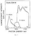
- Fig. 4 shows the PL spectra of the QWW SL at 6.5K and 400K.
- the integral luminescence intensity of the QWW SL is comparable to the (100) SL sample.
- the intensity of the QWW SL does not change with temperature up to 400 K (maximum temperature of the measurement) even at moderate excitation densities.
- the invention provides a method for the direct synthesis of semiconductor quantum well wire structures on high index substrates. Due to its high surface energy the (311) surface breaks up into regular facets having nanometer scale dimensions, which can be directly monitored by RHEED during epitaxial growth. In addition, RHEED dynamics evidences a unique growth mechanism on the stepped surface. Thicker and thinner regions of GaAs and AlAs are built up forming the QWW SL, which was confirmed by distinct energy shifts in the exciton resonances. The 1D character of the QWW SL was reflected in a strong polarization anisotropy of the PL and PLE spectra persisting up to high temperatures. The observed extremely high integrated luminescence intensity, which does not degrade up to 400K, leads to the conclusion that the QWW SL is nearly perfect with only a small degree of disorder.
- the present invention is applicable to many known compositional semiconductor devices with superlattice structures, it only being necessary to grow the devices on a substrate with a ⁇ 311 ⁇ surface in order to realise a quantum well structure in the form of well defined quantum well wires.
- Fig. 5 shows a semiconductor laser device fabricated in accordance with the present invention.
- the semiconductor laser device of Fig. 5 comprises a (311) GaAs n-type substrate 10 onto which there is first grown a GaAs buffer layer 11 of 0.1 microns to 0.5 microns thickness.
- This buffer layer ensures a regular crystallographic structure.
- a layer 12 of Ga 1-x Al x As of n-type material with x typically equal to 0.4 and a thickness of typically 1 ⁇ is grown onto the buffer layer 11.
- This layer 12 is followed by a further layer 13 of Ga 1-y Al y As in which y is typically equal to 0.2.
- Layer 13 has a thickness of approximately 60 ⁇ (or less) and is followed by a further layer 14 of Ga 1-z Al z As with z between 0.1 and 0 and a layer thickness of less than 60 ⁇ (or less).
- This ultra-thin layer 14 is followed by a further ultra-thin layer 15 of the same composition and thickness as the layer 13, i.e. a layer of Ga 1-y Al y As with y approximately equal to 0.2 and a layer thickness of 60 ⁇ (or less).
- These three ultra-thin layers which have a thickness such that size quantization occurs, are then followed by a layer 16 of p-type material which is again Ga 1-x Al x As with x approximately equal to 0.4.
- This layer 16 of p-type material has a thickness of approximately 1 ⁇ and is followed by a thinner layer of GaAs (thickness 0.1 ⁇ to 0.5 ⁇ ) which is doped so that it is a high p+ material (impurity concentration greater than 1018).
- This semiconductor device is provided with first contact means 18 applied to a basal layer of the device, i.e. to the substrate 10.
- Second contact means is provided on an upper layer of the device, namely the GaAs layer 17 and takes the form of a strip-like contact 19.
- the strip-like contact 19 overlies a lasing region 21 of the device.
- the end face 24 of the device is provided with a partially reflective coating illustrated by the shading 25.
- the length should however have dimensions in the ⁇ -range, preferably of several hundred ⁇ m in order to ensure adequately high gain. With other devices it can be of advantage to reduce L to below 500 ⁇ and indeed preferably to below 300 ⁇ .
- the MBE-growth on (211), (311) and (111) oriented GaAs substrates was monitored by RHEED using a 30 keV electron beam at 1° glancing angle, 70-period 46 ⁇ GaAs/41 ⁇ AlAs multilayer structures were grown side by side on a Mo-block with a (100)-GaAs substrate as reference.
- the substrate temperature was 630°C, and the growth rate was 1 ⁇ m/h for GaAs and 0.5 ⁇ /h for AlAs.
- the structural parameters of the samples were determined by double-crystal-x-ray diffraction. Photoluminescence (PL) and photoluminescence excitation (PLE) measurements were performed with the samples mounted in an optical He-flow cryostat. Light from a broadband halogen lamp dispersed by a monochromator, served as excitation source.
- the RHEED-patterns of the (211), (311), and (111) surfaces were recorded along different azimuthal directions.
- a cross-section of the host GaAs crystal viewed along the [011] direction is shown in Fig. 6, with the investigated singular planes indicated.
- the RHEED pattern of the (211) surface shows a reversible faceting of the flat surface at temperatures above 590°C. The transition occurs continuously over a temperature range between 550°C and 590°C.
- the observation of the [01 1 ⁇ ] azimuth (Fig. 7a) exhibits a stepped surface along [ 1 ⁇ 11].
- the methodology is described in reference [23].
- the lateral periodicity of 9.5 ⁇ is deduced from the streak separation and the step height of 3.6 ⁇ from the tilt angle of the intensity maxima along neighbouring streaks together with the lateral periodicity.
- the RHEED pattern of the perpendicular [ 1 ⁇ 11] azimuth (Fig. 7b) shows streaks tilted by 30° to the surface normal, indicating the presence of ⁇ 110 ⁇ facets.
- the surface comprises two sets of ⁇ 110 ⁇ facets along [ 1 ⁇ 11] and alternating (111) terrace planes and (1 ) steps along [01 1 ⁇ ] forming asymmetric pyramides of 3.6 ⁇ height (3 * d211).
- the RHEED pattern of the (311) surface reveals a pronounced streaking with the electron beam along the [01 1 ⁇ ] direction (Fig. 7c) indicating a high density of steps along the perpendicular [ 2 ⁇ 33] direction. Observing the [ 2 ⁇ 33] azimuth parallel to the steps (Fig. 7d), the RHEED pattern images the reciprocal lattice of an almost perfect two level system which is oriented along [ 2 ⁇ 33] (see reference [23]). Contrary to the case of the (211) surface, the RHEED pattern of the stepped (311) surface is stable down to room temperature.
- the lateral periodicity of the stepped surface of 32 ⁇ is determined from the splitting of the (00) streak into sharp satellites and the height of the steps of 10.2 ⁇ from the splitting along its length.
- the (311) surface is composed of (311) terraces of 4 ⁇ width (1 * a110) and two sets of ⁇ 331 ⁇ facets along [ 2 ⁇ 33] corresponding to upward and downward steps of 10.2 ⁇ height (6 * d311).
- the RHEED pattern of the (111) surface shows a pronounced splitting along the (00) streak which corresponds to a surface corrugation of 13.1 ⁇ height.
- the splitting is observed for arbitrary azimuthal directions and, hence, the surface is assumed to break up into symmetric pyramides of 13.1 ⁇ height (4 * d111).
- the MBE grown GaAs/AlAs multilayer samples have a high structural perfection comparable to that of the (100) reference sample, and have the same average GaAs and AlAs layer thicknesses, as determined from the width, intensity and separation of the x-ray diffraction peaks.
- the methodology is described in [24].
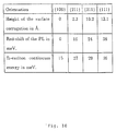
- the observed red shift of the PL peak, with respect to the (100) sample, increases with the height of the surface corrugation for the different orientations (Fig. 3 and Tab.1).
- the red shift is attributed to a heterogenous growth mode on the facets, similar to that observed on non-planar GaAs substrates (as described in reference [25]), which results in the formation of thicker and thinner GaAs (and AlAs) regions, upon the bottom and the top-level of the surface corrugation, respectively.
- the observed enhancement of the light-hole (1h) exciton binding energies also correlates with the height of the surface corrugation as shown in the table of Fig. 10, indicating additional lateral confinement in the GaAs/AlAs multilayer structures, which is introduced by the corrugated interfaces.
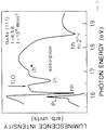
- the 1h exciton binding energies were determined from the energy separation of the 1h- and the excited 1h exciton states observed in the PLE spectra (Fig. 8).
- the 1h-character of the transitions was proved by the measured negative degree of circular polarization, which excludes their origin from "forbidden” transitions. The basis for this proof is described in reference [26].
- the enhanced exiton binding energies give rise to a larger exciton-phonon interaction (see reference [27], due to the increased probability of the excitons created above the bandgap relaxing as a whole. If the detection wavelength is set to the high-energy side of the PL line, strong LO and TA phonon related lines are resolved in the PLE spectra of the (311), (211), and (111) samples (Fig. 8).
- the PLE spectra of the (211) and (311) samples exhibit a pronounced polarization anisotropy of the excitonic resonances.
- the 1h resonance is more pronounced in the spectrum taken with the light polarized parallel to the [011] direction, whereas the heavy-hole (hh) resonance is more pronounced for the polarization perpendicular to [01 1 ⁇ ].
- This behaviour shows the lateral quantization in the [01 1 ⁇ ] direction for both samples.
- the methodology is described in references [28] to [30].
- the polarization anisotropy is more pronounced for the (311) sample compared to the (211) sample owing to the free motion of the carriers allowed along [ 2 ⁇ 33] in agreement with the observed surface structure.
- the residual optical anisotropy of the (211) sample reflects the asymmetric surface structure with the relevant lateral quantization along [01 1 ⁇ ].
- nanometer-scale structures directly during epitaxy is not limited to the orientations discussed here.
- a variety of different structures could be realised also on other crystallographic orientations and material systems, opening a wide field of exciting improved semiconductor devices.
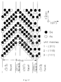
- Fig. 11 shows a crystallographic model of the stepped surface of a QWW SL grown on a (311)-A GaAs surface.
- the crystallographic model shows the stepped surface including the surface atoms with one or more dangling bonds. It clarifies the energetic benefit for the breaking up of the (311) surface in the described manner. It can be seen that the ⁇ 331 ⁇ facets are composed of stripes of alternating (110) and (111) surface configurations corresponding to low-index planes with low surface energy.
- the specified periodicity and step height leads to a nearly perfect stoichiometry of the stepped surface with an As/Ga ratio of 13/12.
- the RHEED intensity dynamics inspected along the [ 2 ⁇ 33] azimuth during the growth of the GaAs/AlAs multilayer structures show pronounced oscillations at the onset of GaAs and AlAs growth.
- the oscillation corresponds to the deposition of three (311) monolayers i.e. lattice planes.
- the intensity approaches the value corresponding to the RHEED pattern of the stable stepped surface during growth.
- the whole sequence is the consequence of a phase change of the surface corrugation as illustrated by the upper (shaded) surface in Fig.
- the complete structure consists of well ordered alternating thicker and thinner regions of GaAs and AlAs oriented along the [ 2 ⁇ 33] direction, and this unique arrangement indeed forms an as-grown QWW SL.
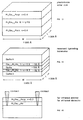
- Figs. 13 to 18 illustrate, for the sake of completeness the typical material layers and thicknesses of a photodiode (or solar cell), of a resonant tunneling transistor, of a far infra-red emitter (or detector), of an optical modulator, of a bipolar transistor and of a high mobility electron transistor respectively.
- all the devices are illustrated as being reallsed in the GaAs or GaAS/Al x Ga 1-x As material systems. It will however be understood that the same types of devices can be realised in other semiconductor material systems and that the actual layer materials used in such devices will be readily apparent to those skilled in the art.
- the devices shown in Figs. 13 to 18 are distinguished from the known prior art devices by the special quantum well structure and by the length and width dimensions which are all equal to or below 500 ⁇ and preferably equal to or below 300 ⁇ . It is not readily possible to give a lower limit for the lateral dimension of the components, however, dimensions of 300 ⁇ or less are already very small and it is unlikely that devices of the kind described will be made with lateral dimensions very much lower than 300 ⁇ - but this is not precluded.
- the doped layers of material are characterised by the letters n- or p- depending on the precise conductivity typed in accordance with standard practice. Layers not designated by n- or p- are assumed to be of intrinsic material, i.e. substantially undoped material. The layer thicknesses given are typical of those used in known prior art components.
- this active layers will generally be manufactured with layer thicknesses under 50 ⁇ but this is not critical.
- the steps in Fig. 17 are for the provision of contacts.
- the anisotropy of the optical properties is a clear proof of the existence of quantum wells and quantum wires.
- the GaAs electron wavefunction has s-symmetry
- the evaluated transition matrix element between electrons and holes in the electric dipole approximation has the symmetry of the hole wavefunction.
- light holes can be described as partly longitudinal waves which travel faster than heavy holes described as transverse waves.
- the evaluation of the Kane matrix element reflects this behaviour.
- the transistions between electron- and heavy-hole states are polarized perpendicular to the hole momentum k, and the transitions between electrons and light holes are partly polarized parallel and perpendicular to k with relative transition intensities of 2/3 and 1/3, respectively.
- the in-plane absorption and luminescence spectra show the heavy-hole exciton only for light polarized perpendicular to z. while the light-hole exciton is much more pronounced for light polarized parallel to z.
- the heavy-hole exciton is expected to be increased with light polarized parallel to the wire axis (s-polarization) and suppressed with light polarized perpendicular to the wire axis (p-polarization), whereas the light-hole exciton is expected to be increased with light polarized perpendicular to the wires and suppressed with light polarized parallel to the wires.
- s-polarization light polarized parallel to the wire axis
- p-polarization light polarized perpendicular to the wire axis
- the degree of polarization will be much lower than for quantum wells because, contrary to the case of the in-plane absorption in quantum wells, the quantization of k is relevant for two directions.
- the existence of GaAs QWW SL on the (311) substrate is confirmed by a strong polarization anisotropy of the excitonic resonances.
- the PL, PLE and the photoluminescence suppression (PLS) spectra of the GaAs buffer layer luminescence were determined for a 66 ⁇ GaAs QWW SL.
- the narrow linewidth of 5 meV of the PL line reflects the high structural perfection of the QWW SL.
- the PLE spectra clearly evidence the 1D confinement. With the light polarized parallel to the wires, the heavy-hole resonance is more pronounced compared to the case with the light polarized perpendicular to the wires, where the light-hole resonance is more intense.
- optical anisotropy is further demonstrated in the PLS spectra.
- this method measures directly the absorption of the QWW SL, and hence the intrinsic polarization anisotropy of the 1D excitonic transitions of the present structure can be determined accurately.
- the observed optical anisotropy is of the order of 15 percent for the heavy-hole exciton resonance and 30 percent for the light-hole exciton resonance. This magnitude of the optical anisotropy is quite realistic for the present structure where the finite barrier heights and the sophisticated shape of the quantum wires has to be considered.
- the corresponding polarization anisotropy also exists in the room temperature luminescence of the QWW SL, where the free electron-heavy-hole and electron-light-hole transitions are observed. It should be noted here, that for the (100) SL reference sample grown side by side, and also for the luminescence of the GaAs buffer layer of the QWW SL, no polarization dependence is observed.
- the in-plane luminescence from the cleavage planes was investigated for the reference SL and the QWW SL.
- the in-plane luminescence of the SL is polarized perpendicular to the z-(growth) direction, whereas the in-plane luminescence of the QWW SL shows a pronounced component which is polarized parallel to the z-direction.
- This component of the luminescence is even more pronounced for the case of the quantum-wires aligned perpendicular to the cleavage plane as compared to the case where the alignment is parallel to this plane.
- This behaviour again demonstrates the influence of the additional 1D confinement on the optical anisotropy and shows that the quantization of k is also relevant for a direction perpendicular to the z-direction.
- the detection wavelength is set to the high-energy side of the luminescence line, sharp lines in the low-excitation intensity (10 ⁇ 6Wcm ⁇ 2) PLE spectra of the QWW SL are resolved.
- the peak energies are separated by 36 meV and 12 meV, and hence the lines correspond to LO and TA phonon related lines.
- the PLE spectra of the reference SL show only one very weak LO phonon line.
- the PLE spectra of the reference SL show only one very weak LO phonon line.
- the appearance of these strong phonon related lines in the QWW SL is thus connected with the additional lateral confinement.
- the additional exciton confinement and the resulting increase of the exciton binding energy up to 30 meV are responsible for this behaviour.
- This binding energy is estimated from the observed energy difference between the ground- and excited heavy-hole exciton states for a 56 ⁇ GaAs QWW SL.
- the additional confinement leads to an increased probability for the excitons created in the 1D continuum to relax and recombine as a whole and, hence, increased interaction of phonons with the excitons is observed.
- strong damping of the phonon lines is expected. It is important to note that this energy threshold provides an estimate of the 2D confinement energy.
- the luminescence line of the QWW SL is shifted to lower energies compared to the (100) reference sample grown side by side.
- This red shift is due to the fact that the luminescence of the QWW SL originates from transitions in the thicker GaAs quantum-wire regions.
- the red shift increases from 3-5 meV for the 66 ⁇ GaAs sample to 40 meV for the 43 ⁇ GaAs sample as can be seen from the corresponding PL spectra at 300K. This variation reflects the increased influence of the interface corrugation for decreases GaAs layer thickness.
- the QWW SL's in general exhibit an extremely high integrated luminescence intensity which is comparable to the (100) reference sample at 6.5K. Even at moderate excitation densities of the order of 10 Wcm ⁇ 2, unity quantum efficiency is achieved. At room temperature, however, the integrated luminescence intensity of the 66 ⁇ GaAs QWW SL is comparable to that of the reference SL sample, whereas for the 43 ⁇ Ga As QWW SL the integrated luminescence intensity is more than one order of magnitude higher than that of the reference SL sample and does not degrade up to 400K. This behaviour again arises from the additional 1D confinement of the present structure.
- the nonradiative interface recombination is in this case strongly suppressed due to the reduced spreading of the carriers which is now possible only in the direction parallel to the wires.
- the average GaAs layer thickness has to be thinner than 66 ⁇ which is in agreement with the estimate of the 1D confinement energy given before. This finding is important for the design of light emitting devices of high efficiency at room temperature.
- SP QWW SL short period
- the SP QWW SL and the reference SP SL become indirect for GaAs and AlAs layer thicknesses below 35 ⁇ .
- the PL spectra shown in Fig. 8a, b reveal a strong zero phonon line and weak phonon sidebands and are typical for the conduction band minimum to be at the X z -point in the AlAs layers.
- the SP QWW SL are of high structural perfection, the PLE spectra reveal a smooth onset and a pronounced overlap with the PL line. This behaviour shows a strong mixing between the - and the X2-minima which is assumed to be due to the interface corrugation.
- the PLE spectra of the SP SL show a sharp onset well separated from the PL line.
- the strong - X2-mixing, even for type-II SP QWW SL with a high energy separation between the - and X-minima results in an integrated luminescence intensity which does not degrade significantly up to room temperature. This finding offers the possibility to fabricate optical devices which work with high efficiency at energies even above the limit for direct-gap GaAS/Al x GX 1-x As SL.
- Additional confirmation of the 1D character of the present QWW SL structure is obtained from the anisotropy of the conductivity of Si-(p-type) modulation-doped GaAs quantum wires.
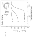
- the samples are mesa etched in an L-shaped geometry shown in the inset of Fig. 12.
- the ratio of the conductivities perpendicular and parallel to the quantum wires as a function of the sample temperature is shown in Fig. 12.
- the curves correspond to different samples with average GaAs layer thicknesses of 80, 50, and 35 ⁇ .
- the average density of holes per unit area deduced from Hall-measurements amounts to 2*1011cm ⁇ 2 for the investigated samples.
- For the 80 ⁇ GaAs quantum wire almost no anisotropic behaviour was observed.
- the anisotropy of the conductivity is increased from 1.6 for the 50 ⁇ GaAs quantum wire to 4.6 for the 35 ⁇ GaAs quantum wire at low temperature, whereby the observed onset of the anisotropy moves to higher temperatures.
- the wavevector of the lateral potential modulation ⁇ /32 ⁇ exceeds the Fermi-wavevector by one order of magnitude, the dispersion relation of the holes is not expected to be altered drastically as in the case of planar superlattices.
- the Fermi-energy is below the 1D confinement energy for holes estimated from the optical investigations. Therefore, it is assumed that the anisotropy of the conductivity in the present structures originates from the confinement of the holes in the quantum wires. From the observed onset of the anisotropy as a function of the temperature, the 1D confinement energies for the holes can be estimated very roughly to be 8meV for the 35 ⁇ GaAs quantum wire and 3meV for the 50 ⁇ GaAs quantum wire. These values are quite close to the values estimated for the 1D confinement energies for the holes from our optical investigations. In this sense, the electrical measurements complete the picture, that has been derived from the optical investigations.
Landscapes
- Engineering & Computer Science (AREA)
- Nanotechnology (AREA)
- Physics & Mathematics (AREA)
- Chemical & Material Sciences (AREA)
- Optics & Photonics (AREA)
- Crystallography & Structural Chemistry (AREA)
- Condensed Matter Physics & Semiconductors (AREA)
- Life Sciences & Earth Sciences (AREA)
- Biophysics (AREA)
- Theoretical Computer Science (AREA)
- Mathematical Physics (AREA)
- General Physics & Mathematics (AREA)
- Electromagnetism (AREA)
- Recrystallisation Techniques (AREA)
- Semiconductor Lasers (AREA)
- Physical Deposition Of Substances That Are Components Of Semiconductor Devices (AREA)
- Light Receiving Elements (AREA)
- Junction Field-Effect Transistors (AREA)
- Photovoltaic Devices (AREA)
- Crystals, And After-Treatments Of Crystals (AREA)
Applications Claiming Priority (4)
| Application Number | Priority Date | Filing Date | Title |
|---|---|---|---|
| EP91101136 | 1991-01-29 | ||
| EP91101136 | 1991-01-29 | ||
| EP91112437 | 1991-07-24 | ||
| EP91112437 | 1991-07-24 |
Publications (1)
| Publication Number | Publication Date |
|---|---|
| EP0535293A1 true EP0535293A1 (fr) | 1993-04-07 |
Family
ID=26128700
Family Applications (1)
| Application Number | Title | Priority Date | Filing Date |
|---|---|---|---|
| EP92100943A Ceased EP0535293A1 (fr) | 1991-01-29 | 1992-01-21 | Procédé de fabrication d'un dispositif semiconducteur compositionnel |
Country Status (3)
| Country | Link |
|---|---|
| US (1) | US5714765A (fr) |
| EP (1) | EP0535293A1 (fr) |
| JP (1) | JPH06224121A (fr) |
Cited By (8)
| Publication number | Priority date | Publication date | Assignee | Title |
|---|---|---|---|---|
| US5518955A (en) * | 1994-02-08 | 1996-05-21 | Mitsubishi Denki Kabushiki Kaisha | Method of fabricating quantum wire |
| US5543354A (en) * | 1993-11-25 | 1996-08-06 | Nippon Telegraph And Telephone Corporation | Method of fabricating a quantum dot structure on a (n11) substrate |
| WO1996030951A1 (fr) * | 1995-03-31 | 1996-10-03 | The University Court Of The University Of Glasgow | Photoemetteurs et photodetecteurs |
| US5614435A (en) * | 1994-10-27 | 1997-03-25 | The Regents Of The University Of California | Quantum dot fabrication process using strained epitaxial growth |
| EP1130657A2 (fr) * | 1999-06-09 | 2001-09-05 | Universidad Politecnica De Madrid | Cellule solaire photovoltaique a semi-conducteur avec bande intermediaire |
| EP1029359A4 (fr) * | 1997-11-10 | 2007-06-06 | Don L Kendall | Cretes et pointes quantiques |
| US7948822B2 (en) | 2006-12-08 | 2011-05-24 | Technische Universitat Berlin | Memory cell, and method for storing data |
| US7960715B2 (en) | 2008-04-24 | 2011-06-14 | University Of Iowa Research Foundation | Semiconductor heterostructure nanowire devices |
Families Citing this family (25)
| Publication number | Priority date | Publication date | Assignee | Title |
|---|---|---|---|---|
| JPH07193324A (ja) * | 1993-12-27 | 1995-07-28 | Nec Corp | 半導体量子井戸レーザー構造 |
| DE19604348C2 (de) * | 1996-02-07 | 2003-10-23 | Deutsche Telekom Ag | Verfahren zur Herstellung einer kalibrierten Längenskala im Nanometerbereich für technische Geräte, die der hochauflösenden bis ultrahochauflösenden Abbildung von Strukturen dienen |
| JPH1065145A (ja) * | 1996-08-22 | 1998-03-06 | Hitachi Ltd | 電導性原子サイズ細線および原子サイズスイッチ |
| JP3955367B2 (ja) * | 1997-09-30 | 2007-08-08 | フィリップス ルミレッズ ライティング カンパニー リミテッド ライアビリティ カンパニー | 光半導体素子およびその製造方法 |
| AU2262701A (en) * | 1999-12-13 | 2001-06-18 | Regents Of The University Of California, The | Semiconductor device with gigantic photon-photon interactions |
| DE10019712A1 (de) * | 2000-04-20 | 2001-10-25 | Max Planck Gesellschaft | Verfahren zur Herstellung von periodischen Materialstrukturen |
| US6816525B2 (en) | 2000-09-22 | 2004-11-09 | Andreas Stintz | Quantum dot lasers |
| US6600169B2 (en) * | 2000-09-22 | 2003-07-29 | Andreas Stintz | Quantum dash device |
| WO2002071562A2 (fr) * | 2001-03-02 | 2002-09-12 | Science & Technology Corporation @ Unm | Laser a points quantiques et a cavite verticale emettant par la surface |
| WO2003023817A2 (fr) * | 2001-07-20 | 2003-03-20 | The Board Of Trustees Of The University Of Illinois | Procede de formation de points quantiques semi-conducteurs presentant une meilleure stabilite structurelle et morphologique |
| US6924501B2 (en) * | 2001-09-27 | 2005-08-02 | National Institute Of Advanced Industrial Science And Technology | Quantum logic gate and quantum logic operation method using exciton |
| US7385262B2 (en) * | 2001-11-27 | 2008-06-10 | The Board Of Trustees Of The Leland Stanford Junior University | Band-structure modulation of nano-structures in an electric field |
| DE10201126A1 (de) * | 2002-01-09 | 2003-07-24 | Infineon Technologies Ag | Optoelektronisches Bauelement und Verfahren zu seiner Herstellung |
| US6853761B2 (en) * | 2002-01-09 | 2005-02-08 | Infineon Technologies Ag | Optoelectronic module |
| DE10203696A1 (de) * | 2002-01-09 | 2003-07-24 | Infineon Technologies Ag | Optoelektronisches Bauelement |
| DE10201124A1 (de) * | 2002-01-09 | 2003-07-24 | Infineon Technologies Ag | Optoelektronisches Bauelement und Verfahren zu seiner Herstellung |
| RU2210836C1 (ru) * | 2002-02-11 | 2003-08-20 | Рязанская государственная радиотехническая академия | Способ формирования наноостровков германия на вицинальной поверхности кремния |
| DE10227168A1 (de) * | 2002-06-18 | 2004-01-15 | Infineon Technologies Ag | Vorrichtung zur optischen Signalübertragung, Verfahren zur optischen Signalübertragung und optischer Modulator |
| DE10260378A1 (de) * | 2002-12-16 | 2004-07-08 | Infineon Technologies Ag | Optoelektronisches Bauelement mit einer Pulserzeugungseinrichtung |
| US7282732B2 (en) * | 2003-10-24 | 2007-10-16 | Stc. Unm | Quantum dot structures |
| FR2876498B1 (fr) * | 2004-10-12 | 2008-03-14 | Commissariat Energie Atomique | Procede de realisation d'heterostructures resonnantes a transport planaire |
| US8829336B2 (en) * | 2006-05-03 | 2014-09-09 | Rochester Institute Of Technology | Nanostructured quantum dots or dashes in photovoltaic devices and methods thereof |
| WO2007131126A2 (fr) * | 2006-05-03 | 2007-11-15 | Rochester Institute Of Technology | Dispositifs photovoltaïques à jonctions multiples possédant des éléments d'enrichissement spectral nanostructurés et procédés associés |
| US8431460B2 (en) * | 2011-05-27 | 2013-04-30 | United Microelectronics Corp. | Method for fabricating semiconductor device |
| US20220416112A1 (en) * | 2021-06-29 | 2022-12-29 | Alliance For Sustainable Energy, Llc | Control of surface morphology of spalled (110) iii-v substrate surfaces |
Citations (3)
| Publication number | Priority date | Publication date | Assignee | Title |
|---|---|---|---|---|
| EP0165419A2 (fr) * | 1984-05-29 | 1985-12-27 | Kabushiki Kaisha Meidensha | Dispositif de commutation à semi-conducteur comportant une structure de gâchette enterrée |
| EP0244140A2 (fr) * | 1986-04-21 | 1987-11-04 | Hitachi, Ltd. | Dispositif semi-conducteur à structure périodique |
| DE3728524A1 (de) * | 1986-08-28 | 1988-03-10 | Sony Corp | Hochgeschwindigkeits-halbleiterbauteil und verfahren zu seiner herstellung |
Family Cites Families (6)
| Publication number | Priority date | Publication date | Assignee | Title |
|---|---|---|---|---|
| JPS6140082A (ja) * | 1984-07-31 | 1986-02-26 | Sharp Corp | 半導体装置 |
| US4872046A (en) * | 1986-01-24 | 1989-10-03 | University Of Illinois | Heterojunction semiconductor device with <001> tilt |
| US4974036A (en) * | 1988-02-09 | 1990-11-27 | Bell Communications Research, Inc. | Semiconductor superlattice heterostructures on nonplanar substrates |
| JPH02139970A (ja) * | 1988-11-21 | 1990-05-29 | Nippon Telegr & Teleph Corp <Ntt> | 半導体量子箱の作製方法 |
| NL8900767A (nl) * | 1989-03-29 | 1990-10-16 | Philips Nv | Halfgeleiderinrichting met eendimensionale doteringsgeleiders en werkwijze ter vervaardiging van een dergelijke halfgeleiderinrichting. |
| US5065200A (en) * | 1989-12-21 | 1991-11-12 | Bell Communications Research, Inc. | Geometry dependent doping and electronic devices produced thereby |
-
1992
- 1992-01-21 EP EP92100943A patent/EP0535293A1/fr not_active Ceased
- 1992-01-29 JP JP4038528A patent/JPH06224121A/ja not_active Withdrawn
-
1994
- 1994-10-26 US US08/329,802 patent/US5714765A/en not_active Expired - Fee Related
Patent Citations (3)
| Publication number | Priority date | Publication date | Assignee | Title |
|---|---|---|---|---|
| EP0165419A2 (fr) * | 1984-05-29 | 1985-12-27 | Kabushiki Kaisha Meidensha | Dispositif de commutation à semi-conducteur comportant une structure de gâchette enterrée |
| EP0244140A2 (fr) * | 1986-04-21 | 1987-11-04 | Hitachi, Ltd. | Dispositif semi-conducteur à structure périodique |
| DE3728524A1 (de) * | 1986-08-28 | 1988-03-10 | Sony Corp | Hochgeschwindigkeits-halbleiterbauteil und verfahren zu seiner herstellung |
Non-Patent Citations (11)
| Title |
|---|
| IBM TECHNICAL DISCLOSURE BULLETIN. vol. 29, no. 5, 5 October 1986, NEW YORK US pages 2229 - 2231; 'Semiconductor two-dimensional hole gas heterostructures' * |
| JOURNAL OF APPLIED PHYSICS. vol. 59, no. 2, 15 January 1986, NEW YORK US pages 488 - 494; S.SUBBANNA ET AL.: 'Molecular-beam-epitaxial growth and selected properties of GaAs layers and GaAs/(Al,Ga)As superlattices with the (211) orientation' * |
| JOURNAL OF APPLIED PHYSICS. vol. 60, no. 5, 1 September 1986, NEW YORK US pages 1834 - 1835; W.I.WANG ET AL.: 'High mobility two-dimensional hole gas in AlGaAs/GaAs heterojunction' * |
| PHYSICAL REVIEW LETTERS. vol. 60, no. 6, 8 February 1988, NEW YORK US pages 535 - 537; M.A.REED ET AL.: 'Observation of discrete electronic states in a zero-dimensional semiconductor nanostructure' * |
| PHYSICAL REVIEW LETTERS. vol. 62, no. 4, 23 January 1989, NEW YORK US pages 466 - 469; M.TSUCHIYA ET AL.: 'Optical anisotropy in a quantum-well-wire array with two-dimensional quantum confinement' * |
| PHYSICAL REVIEW LETTERS. vol. 63, no. 19, 6 November 1989, NEW YORK US pages 2124 - 2127; M.KOHL ET AL.: 'One-dimensional magnetoexcitons in GaAs/AlGaAs quantum wires' * |
| PHYSICAL REVIEW LETTERS. vol. 63, no. 4, 24 July 1989, NEW YORK US pages 430 - 433; E.KAPON ET AL.: 'Stimulated emission in semiconductor quantum wire heterostructures' * |
| PHYSICAL REVIEW LETTERS. vol. 64, no. 9, 26 February 1990, NEW YORK US pages 1055 - 1058; R.ZACHAI ET AL.: 'Photoluminescence in short-period Si/Ge strained-layer superlattices' * |
| PHYSICAL REVIEW LETTERS. vol. 67, no. 27, 30 December 1991, NEW YORK US pages 3812 - 3815; R.NÖTZEL ET AL.: 'Direct synthesis of corrugated superlattices on non-(100)-oriented surfaces' * |
| PHYSICAL REVIEW, B. SOLID STATE. vol. 38, no. 2, 15 July 1988, NEW YORK US pages 1526 - 1528; T.HAYAKAWA ET AL.: 'Observation of the 2s state excitons in (111)-oriented GaAs/AlGaAs quantum-well structures' * |
| PHYSICAL REVIEW, B. SOLID STATE. vol. 39, no. 18, 15 June 1989, NEW YORK US pages 13533 - 13536; T. EL KHALIFI ET AL.: 'Dependence of the light-hole - heavy-hole splitting on layer thickness and substrate orientation in GaAs-(GaAl)As single quantum wells' * |
Cited By (11)
| Publication number | Priority date | Publication date | Assignee | Title |
|---|---|---|---|---|
| US5543354A (en) * | 1993-11-25 | 1996-08-06 | Nippon Telegraph And Telephone Corporation | Method of fabricating a quantum dot structure on a (n11) substrate |
| EP0665578A3 (fr) * | 1993-11-25 | 1996-10-30 | Nippon Telegraph & Telephone | Structure à semiconducteur et méthode de fabrication. |
| US5518955A (en) * | 1994-02-08 | 1996-05-21 | Mitsubishi Denki Kabushiki Kaisha | Method of fabricating quantum wire |
| US5684823A (en) * | 1994-02-08 | 1997-11-04 | Mitsubishi Denki Kabushiki Kaisha | Method of fabricating a diffraction grating and a distributed feedback semiconductor laser incorporating the diffraction grating |
| US5614435A (en) * | 1994-10-27 | 1997-03-25 | The Regents Of The University Of California | Quantum dot fabrication process using strained epitaxial growth |
| WO1996030951A1 (fr) * | 1995-03-31 | 1996-10-03 | The University Court Of The University Of Glasgow | Photoemetteurs et photodetecteurs |
| EP1029359A4 (fr) * | 1997-11-10 | 2007-06-06 | Don L Kendall | Cretes et pointes quantiques |
| EP1130657A2 (fr) * | 1999-06-09 | 2001-09-05 | Universidad Politecnica De Madrid | Cellule solaire photovoltaique a semi-conducteur avec bande intermediaire |
| US7948822B2 (en) | 2006-12-08 | 2011-05-24 | Technische Universitat Berlin | Memory cell, and method for storing data |
| US7960715B2 (en) | 2008-04-24 | 2011-06-14 | University Of Iowa Research Foundation | Semiconductor heterostructure nanowire devices |
| US8124518B2 (en) | 2008-04-24 | 2012-02-28 | University Of Iowa Research Foundation | Semiconductor heterostructure nanowire devices |
Also Published As
| Publication number | Publication date |
|---|---|
| US5714765A (en) | 1998-02-03 |
| JPH06224121A (ja) | 1994-08-12 |
Similar Documents
| Publication | Publication Date | Title |
|---|---|---|
| US5714765A (en) | Method of fabricating a compositional semiconductor device | |
| Nötzel et al. | Semiconductor quantum-wire structures directly grown on high-index surfaces | |
| Maximov et al. | Tuning quantum dot properties by activated phase separation of an InGa (Al) As alloy grown on InAs stressors | |
| Arakawa | Progress in GaN-based quantum dots for optoelectronics applications | |
| Pearah et al. | AlGaInP multiple quantum wire heterostructure lasers prepared by the strain-induced lateral-layer ordering process | |
| Zhang et al. | Naturally formed ZnCdSe quantum dots on ZnSe (110) surfaces | |
| Chou et al. | Ga x In1− x As multiple‐quantum‐wire lasers grown by the strain‐induced lateral‐layer ordering process | |
| Henini | Properties and applications of quantum dot heterostructures grown by molecular beam epitaxy | |
| ARAKAWA et al. | Progress in GaN-based nanostructures for blue light emitting quantum dot lasers and vertical cavity surface emitting lasers | |
| Shen et al. | High-quality InGaN/GaN multiple quantum wells grown on Ga-polarity GaN by plasma-assisted molecular-beam epitaxy | |
| Tan et al. | Quantum dots and nanowires grown by metal–organic chemical vapor deposition for optoelectronic device applications | |
| Vaccaro et al. | Spontaneous Formation of Nanostructures in I nx G a 1-x A s Epilayers Grown by Molecular Beam Epitaxy on GaAs Non-(100)-oriented Substrates | |
| Ustinov | Quantum dot structures: Fabrication technology and control of parameters | |
| Vallejo et al. | Tensile-strained InGaAs quantum dots with interband emission in the mid-infrared | |
| Ustinov et al. | Arrays of strained InAs quantum dots in an (In Ga) As matrix, grown on InP substrates by molecular-beam epitaxy | |
| Notzel et al. | Man-made low-dimensional solids: new challenges in microstructure material science | |
| Pearah et al. | Formation of multiple quantum wires by strain-induced lateral-layer ordering process | |
| Pearah et al. | Strained AlGaInP quantum wire lasers | |
| Solov’ev et al. | GaAs in GaSb: Strained nanostructures for mid-infrared optoelectronics | |
| Khatab | Optical properties of nanostructured semiconductors grown by MBE on non-conventional GaAs substrates | |
| Carrington et al. | Type II InSb/InAs quantum dot structures grown by molecular beam epitaxy using Sb2 and As2 fluxes | |
| Ploog et al. | Direct Fabrication of III–V Semiconductor Quantum Dots and Quantum Wires by Molecular Beam Epitaxy | |
| Tsurumachi et al. | Photoluminescence and Photoluminescence Excitation Spectra of Strained High-Density InGaAs/Al x Ga1-x As Quantum Wire Structures on Submicron Grating | |
| Henini | Self-Assembled Quantum Dots for Optoelectronic Devices: Progress and Challenges | |
| LEDENTSOV | Abraham F. Ioffe Institute, 194021, St. Petersburg, Russia. e-mail: leden@ w422zz. physik. tu-berlin. de |
Legal Events
| Date | Code | Title | Description |
|---|---|---|---|
| PUAI | Public reference made under article 153(3) epc to a published international application that has entered the european phase |
Free format text: ORIGINAL CODE: 0009012 |
|
| AK | Designated contracting states |
Kind code of ref document: A1 Designated state(s): DE FR GB IT NL |
|
| 17Q | First examination report despatched |
Effective date: 19950814 |
|
| STAA | Information on the status of an ep patent application or granted ep patent |
Free format text: STATUS: THE APPLICATION HAS BEEN REFUSED |
|
| 18R | Application refused |
Effective date: 20000219 |