EP0535882A1 - Procédé pour la fabrication d'un empaquetage de puce semi-conductrice - Google Patents
Procédé pour la fabrication d'un empaquetage de puce semi-conductrice Download PDFInfo
- Publication number
- EP0535882A1 EP0535882A1 EP92308799A EP92308799A EP0535882A1 EP 0535882 A1 EP0535882 A1 EP 0535882A1 EP 92308799 A EP92308799 A EP 92308799A EP 92308799 A EP92308799 A EP 92308799A EP 0535882 A1 EP0535882 A1 EP 0535882A1
- Authority
- EP
- European Patent Office
- Prior art keywords
- dam
- mold compound
- dam bar
- bond
- semiconductor chip
- Prior art date
- Legal status (The legal status is an assumption and is not a legal conclusion. Google has not performed a legal analysis and makes no representation as to the accuracy of the status listed.)
- Granted
Links
Images
Classifications
-
- H—ELECTRICITY
- H10—SEMICONDUCTOR DEVICES; ELECTRIC SOLID-STATE DEVICES NOT OTHERWISE PROVIDED FOR
- H10W—GENERIC PACKAGES, INTERCONNECTIONS, CONNECTORS OR OTHER CONSTRUCTIONAL DETAILS OF DEVICES COVERED BY CLASS H10
- H10W70/00—Package substrates; Interposers; Redistribution layers [RDL]
- H10W70/40—Leadframes
- H10W70/421—Shapes or dispositions
-
- H—ELECTRICITY
- H10—SEMICONDUCTOR DEVICES; ELECTRIC SOLID-STATE DEVICES NOT OTHERWISE PROVIDED FOR
- H10W—GENERIC PACKAGES, INTERCONNECTIONS, CONNECTORS OR OTHER CONSTRUCTIONAL DETAILS OF DEVICES COVERED BY CLASS H10
- H10W70/00—Package substrates; Interposers; Redistribution layers [RDL]
- H10W70/01—Manufacture or treatment
- H10W70/04—Manufacture or treatment of leadframes
- H10W70/048—Mechanical treatments, e.g. punching, cutting, deforming or cold welding
Definitions
- This invention relates, in general, to processing of semiconductor packages, including, but not limited to, a method of removing dam bars from the leads of a semiconductor chip package.
- Some semiconductor chips or integrated circuits are packaged by bonding the chip to a leadframe having leads.
- the leadframe is then encapsulated by a mold compound typically comprised of a plastic.
- dam bars are formed on the leads near the portion of the lead frame which is to be encapsulated.
- mold compound fills the area between the leads up to the dam bars.
- the dam bars act to stop or prevent the mold compound from flowing out between the leads past the dam bars.
- a small portion of excess mold compound is formed on the lead adjacent the area on which the semiconductor chip is bonded on the lead frame.
- the dam bars also keep the leads coplanar and properly aligned during the assembly process.
- Another method of removing the dam bars and the excess mold compound entails using a laser trimming system.
- This laser trimming system may prevent cracks or chips to the adjacent mold compound, however, it is much more complicated and expensive to use. It would be desirable to prevent chipping or cracking of the mold compound by using a less costly method.
- a method of processing a semiconductor chip package is disclosed.
- This chip package has a dam bar formed on a lead and excess mold compound abutting the dam bar.
- the dam bar and excess mold compound form a bond.
- the dam bar is removed by first moving the dam bar in a manner in which the bond between the dam bar and the excess mold compound is broken and then the dam bar is moved furtherto completely remove the dam barfrom the lead.
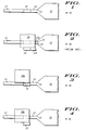
- FIG. 1 illustrates a side-view of a semiconductor package 10 which is to be processed in the present invention.
- a mold compound 11 encapsulates a lead frame having at least one lead 17.
- excess mold compound 12 is formed between portions of lead 17.
- the distinction between excess mold compound 12 and mold compound 11 is illustrated by dotted line 13 for convenience only.
- Adam bar 15 is formed as a part of lead 17 in order to maintain lead coplanarity and to prevent excess mold compound 12 from being formed past dam bar 15.
- the encapsulation process described above is well known in the art.
- FIG. 2 illustrates a side-view of semiconductor package 10 shown in FIG. 1 processed according to a prior art method.
- a mechanical tool called a punch 19 is used to "punch" out dam bar 15 and a portion of excess mold compound 12a simultaneously.
- excess mold compound 12 is broken into portion 12a removed from lead 17 and a portion 12b which remains on lead 17 attached to mold compound 11.
- chips and or cracks 21 may be formed in mold compound 11.
- plating and/or other solder materials may be formed in crack 21 causing reliability problems or electrical failures in the semiconductor chip encapsulated by mold compound 11.
- FIG. 3 illustrates semiconductor package 10 of FIG. 1 processed according to an embodiment of the present invention in a beginning stage of processing.
- a punch 19a is also used in the present invention. However, in the present invention, punch 19a is used only to move dam bar 15 so that a bond between dam bar 15 and excess mold compound 12 is broken while semiconductor package 10 is in a first position. This slight movement may also be performed by other mechanical tools.
- a movement by punch 19a of a predetermined percentage of the thickness of dambar 15 is necessary to break the bond between dam bar 15 and excess mold compound 12. This predetermined percentage may be, for example, between approximately 30 and 50 percent of the thickness of dam bar 15.
- FIG. 4 illustrates the structure of FIG. 3 further along in processing.
- Semiconductor package 10 is moved to a second position, then dam bar 15 is completely removed by a punch 19b by moving dam bar 15 further away from lead 17.
- excess mold compound 12 is left undamaged.
- no cracks or chips are created in mold compound 11.
- Excess mold compound 12 may remain on lead 17 without hindering the performance of the semiconductor chip housed in semiconductor package 10.
- two punches, 19a and 19b must be used because each punch may only move to one level.
- dam bar 15 is removed using at least two movements of dam bar 15 rather than one continuous movement.
- a dam bar can be removed from a lead of a semiconductor package without having cracks or chips formed in the mold compound which may subsequently cause reliability problems or electrical failures.
- dam bar 15 A slight movement of dam bar 15 to break the bond between dam bar 15 and excess mold compound 12 prevents the formation of chips or cracks upon subsequently completely removing dam bar 15 from lead 17.
Landscapes
- Lead Frames For Integrated Circuits (AREA)
- Encapsulation Of And Coatings For Semiconductor Or Solid State Devices (AREA)
Applications Claiming Priority (2)
| Application Number | Priority Date | Filing Date | Title |
|---|---|---|---|
| US76759391A | 1991-09-30 | 1991-09-30 | |
| US767593 | 1991-09-30 |
Publications (2)
| Publication Number | Publication Date |
|---|---|
| EP0535882A1 true EP0535882A1 (fr) | 1993-04-07 |
| EP0535882B1 EP0535882B1 (fr) | 2001-11-14 |
Family
ID=25079961
Family Applications (1)
| Application Number | Title | Priority Date | Filing Date |
|---|---|---|---|
| EP92308799A Expired - Lifetime EP0535882B1 (fr) | 1991-09-30 | 1992-09-28 | Procédé pour la fabrication d'un empaquetage de puce semi-conductrice |
Country Status (10)
| Country | Link |
|---|---|
| US (1) | US5690877A (fr) |
| EP (1) | EP0535882B1 (fr) |
| JP (1) | JP3399988B2 (fr) |
| KR (1) | KR100248551B1 (fr) |
| CN (1) | CN1073044A (fr) |
| CZ (1) | CZ282517B6 (fr) |
| DE (1) | DE69232200T2 (fr) |
| MX (1) | MX9205128A (fr) |
| SG (1) | SG46266A1 (fr) |
| SK (1) | SK298792A3 (fr) |
Cited By (2)
| Publication number | Priority date | Publication date | Assignee | Title |
|---|---|---|---|---|
| US5886397A (en) * | 1996-09-05 | 1999-03-23 | International Rectifier Corporation | Crushable bead on lead finger side surface to improve moldability |
| US5898216A (en) * | 1995-11-14 | 1999-04-27 | Sgs-Thomson Microelectronics S.A. | Micromodule with protection barriers and a method for manufacturing the same |
Citations (3)
| Publication number | Priority date | Publication date | Assignee | Title |
|---|---|---|---|---|
| EP0090503A2 (fr) * | 1982-03-25 | 1983-10-05 | Texas Instruments Incorporated | Appareil et procédé pour encapsuler un dispositif semi-conducteur |
| EP0330512A2 (fr) * | 1988-02-24 | 1989-08-30 | Fujitsu Limited | La fabrication de composants électroniques à l'aide de cadres de conducteurs |
| EP0397320A2 (fr) * | 1989-04-13 | 1990-11-14 | Texas Instruments Incorporated | Circuit intégré encapsulé comprenant un cadre conducteur |
Family Cites Families (15)
| Publication number | Priority date | Publication date | Assignee | Title |
|---|---|---|---|---|
| US3539675A (en) * | 1965-10-22 | 1970-11-10 | Motorola Inc | Method for encapsulating semiconductor devices |
| US4109373A (en) * | 1975-03-10 | 1978-08-29 | General Electric Company | Method for manufacturing semiconductor devices |
| US4451973A (en) * | 1981-04-28 | 1984-06-05 | Matsushita Electronics Corporation | Method for manufacturing a plastic encapsulated semiconductor device and a lead frame therefor |
| JPS5896921U (ja) * | 1981-12-24 | 1983-07-01 | トヨタ自動車株式会社 | インサート成形装置 |
| JPS59135753A (ja) * | 1983-01-25 | 1984-08-04 | Toshiba Corp | 半導体装置とその製造方法 |
| US4504427A (en) * | 1983-06-17 | 1985-03-12 | At&T Bell Laboratories | Solder preform stabilization for lead frames |
| JPS60176259A (ja) * | 1984-02-22 | 1985-09-10 | Toshiba Corp | 樹脂封止形半導体装置の製造方法 |
| JPS6147658A (ja) * | 1984-08-14 | 1986-03-08 | Nec Kansai Ltd | 半導体装置の製造方法 |
| US4615857A (en) * | 1984-11-30 | 1986-10-07 | Motorola, Inc. | Encapsulation means and method for reducing flash |
| US4862586A (en) * | 1985-02-28 | 1989-09-05 | Michio Osada | Lead frame for enclosing semiconductor chips with resin |
| JPS62128163A (ja) * | 1985-11-29 | 1987-06-10 | Nec Corp | リ−ドフレ−ム |
| US4778146A (en) * | 1987-03-20 | 1988-10-18 | Asm Fico | Leadframe for flash-free insert molding and method therefor |
| US4874722A (en) * | 1987-04-16 | 1989-10-17 | Texas Instruments Incorporated | Process of packaging a semiconductor device with reduced stress forces |
| US4915607A (en) * | 1987-09-30 | 1990-04-10 | Texas Instruments Incorporated | Lead frame assembly for an integrated circuit molding system |
| US4946518A (en) * | 1989-03-14 | 1990-08-07 | Motorola, Inc. | Method for improving the adhesion of a plastic encapsulant to copper containing leadframes |
-
1992
- 1992-09-08 MX MX9205128A patent/MX9205128A/es not_active IP Right Cessation
- 1992-09-15 KR KR1019920016706A patent/KR100248551B1/ko not_active Expired - Lifetime
- 1992-09-22 JP JP27670892A patent/JP3399988B2/ja not_active Expired - Fee Related
- 1992-09-24 CN CN92110849.4A patent/CN1073044A/zh active Pending
- 1992-09-28 SG SG1996001750A patent/SG46266A1/en unknown
- 1992-09-28 DE DE69232200T patent/DE69232200T2/de not_active Expired - Fee Related
- 1992-09-28 EP EP92308799A patent/EP0535882B1/fr not_active Expired - Lifetime
- 1992-09-30 CZ CS922987A patent/CZ282517B6/cs not_active IP Right Cessation
- 1992-09-30 SK SK2987-92A patent/SK298792A3/sk unknown
-
1995
- 1995-03-16 US US08/405,563 patent/US5690877A/en not_active Expired - Lifetime
Patent Citations (3)
| Publication number | Priority date | Publication date | Assignee | Title |
|---|---|---|---|---|
| EP0090503A2 (fr) * | 1982-03-25 | 1983-10-05 | Texas Instruments Incorporated | Appareil et procédé pour encapsuler un dispositif semi-conducteur |
| EP0330512A2 (fr) * | 1988-02-24 | 1989-08-30 | Fujitsu Limited | La fabrication de composants électroniques à l'aide de cadres de conducteurs |
| EP0397320A2 (fr) * | 1989-04-13 | 1990-11-14 | Texas Instruments Incorporated | Circuit intégré encapsulé comprenant un cadre conducteur |
Non-Patent Citations (2)
| Title |
|---|
| PATENT ABSTRACTS OF JAPAN vol. 10, no. 205 (E-420)17 July 1986 & JP-A-61 047 658 ( NEC ) 8 March 1986 * |
| PATENT ABSTRACTS OF JAPAN vol. 11, no. 351 (E-557)17 November 1987 & JP-A-62 128 163 ( NEC ) 10 June 1987 * |
Cited By (4)
| Publication number | Priority date | Publication date | Assignee | Title |
|---|---|---|---|---|
| US5898216A (en) * | 1995-11-14 | 1999-04-27 | Sgs-Thomson Microelectronics S.A. | Micromodule with protection barriers and a method for manufacturing the same |
| US6071758A (en) * | 1995-11-14 | 2000-06-06 | Sgs-Thomson Microelectronics S.A. | Process for manufacturing a chip card micromodule with protection barriers |
| US5886397A (en) * | 1996-09-05 | 1999-03-23 | International Rectifier Corporation | Crushable bead on lead finger side surface to improve moldability |
| US6078098A (en) * | 1996-09-05 | 2000-06-20 | International Rectifier Corp. | Crushable bead on lead finger side surface to improve moldability |
Also Published As
| Publication number | Publication date |
|---|---|
| CZ298792A3 (en) | 1993-04-14 |
| MX9205128A (es) | 1993-04-01 |
| EP0535882B1 (fr) | 2001-11-14 |
| KR100248551B1 (ko) | 2000-03-15 |
| JP3399988B2 (ja) | 2003-04-28 |
| US5690877A (en) | 1997-11-25 |
| SK298792A3 (en) | 1994-11-09 |
| SG46266A1 (en) | 1998-02-20 |
| CN1073044A (zh) | 1993-06-09 |
| CZ282517B6 (cs) | 1997-07-16 |
| DE69232200T2 (de) | 2002-06-06 |
| DE69232200D1 (de) | 2001-12-20 |
| JPH05206182A (ja) | 1993-08-13 |
Similar Documents
| Publication | Publication Date | Title |
|---|---|---|
| US11562929B2 (en) | Sawn leadless package having wettable flank leads | |
| EP3440697B1 (fr) | Boîtier plat sans conducteurs à conducteurs de contact améliorés | |
| US5070039A (en) | Method of making an integrated circuit using a pre-served dam bar to reduce mold flash and to facilitate flash removal | |
| US3436810A (en) | Method of packaging integrated circuits | |
| EP0989608A3 (fr) | Boítier en plastique pour circuit intégré et son procédé de fabrication | |
| JP2002064114A (ja) | 半導体装置及びその製造方法 | |
| US5690877A (en) | Method of processing a semiconductor chip package | |
| JPS618960A (ja) | リ−ドフレ−ム | |
| US6303983B1 (en) | Apparatus for manufacturing resin-encapsulated semiconductor devices | |
| US4592131A (en) | Method for manufacturing resin-sealed semiconductor device | |
| CN113394187B (zh) | 无引线半导体封装件以及制造方法 | |
| JP2686240B2 (ja) | 樹脂封止型半導体装置の製造方法 | |
| US20250022831A1 (en) | Semiconductor packages with wettable flanks and related methods | |
| JP2826508B2 (ja) | 半導体装置の製造装置 | |
| US20240379506A1 (en) | Electronic device with improved leadframe trimming process | |
| JPH04293243A (ja) | 樹脂封止用金型装置とゲートの切断方法 | |
| KR920006185B1 (ko) | 접합형 리드 프레임을 사용한 ic 제조방법 | |
| KR940000745B1 (ko) | 와이어 본딩방법 | |
| KR200168394Y1 (ko) | 반도체 패키지의 리드 프레임 | |
| JPS63302545A (ja) | 樹脂封止型半導体リ−ドフレ−ム | |
| JPH0444425B2 (fr) | ||
| KR100342815B1 (ko) | 반도체패키지용 핀치컷 작업공정 및 구조 | |
| JPH11319977A (ja) | リードフレーム打抜き用金型及びリード切断方法 | |
| CN118737855A (zh) | 具有可浸润侧翼的半导体封装件及相关方法 | |
| JP2007095852A (ja) | 小型電子部品の製造方法 |
Legal Events
| Date | Code | Title | Description |
|---|---|---|---|
| PUAI | Public reference made under article 153(3) epc to a published international application that has entered the european phase |
Free format text: ORIGINAL CODE: 0009012 |
|
| AK | Designated contracting states |
Kind code of ref document: A1 Designated state(s): DE FR GB IT |
|
| 17P | Request for examination filed |
Effective date: 19930930 |
|
| 17Q | First examination report despatched |
Effective date: 19950421 |
|
| GRAG | Despatch of communication of intention to grant |
Free format text: ORIGINAL CODE: EPIDOS AGRA |
|
| GRAG | Despatch of communication of intention to grant |
Free format text: ORIGINAL CODE: EPIDOS AGRA |
|
| GRAH | Despatch of communication of intention to grant a patent |
Free format text: ORIGINAL CODE: EPIDOS IGRA |
|
| GRAH | Despatch of communication of intention to grant a patent |
Free format text: ORIGINAL CODE: EPIDOS IGRA |
|
| ITF | It: translation for a ep patent filed | ||
| GRAA | (expected) grant |
Free format text: ORIGINAL CODE: 0009210 |
|
| AK | Designated contracting states |
Kind code of ref document: B1 Designated state(s): DE FR GB IT |
|
| REF | Corresponds to: |
Ref document number: 69232200 Country of ref document: DE Date of ref document: 20011220 |
|
| REG | Reference to a national code |
Ref country code: GB Ref legal event code: IF02 |
|
| PLBE | No opposition filed within time limit |
Free format text: ORIGINAL CODE: 0009261 |
|
| 26N | No opposition filed | ||
| REG | Reference to a national code |
Ref country code: GB Ref legal event code: 732E |
|
| PGFP | Annual fee paid to national office [announced via postgrant information from national office to epo] |
Ref country code: GB Payment date: 20060804 Year of fee payment: 15 |
|
| PGFP | Annual fee paid to national office [announced via postgrant information from national office to epo] |
Ref country code: FR Payment date: 20060906 Year of fee payment: 15 |
|
| PGFP | Annual fee paid to national office [announced via postgrant information from national office to epo] |
Ref country code: DE Payment date: 20060929 Year of fee payment: 15 |
|
| PGFP | Annual fee paid to national office [announced via postgrant information from national office to epo] |
Ref country code: IT Payment date: 20060930 Year of fee payment: 15 |
|
| REG | Reference to a national code |
Ref country code: FR Ref legal event code: TP |
|
| GBPC | Gb: european patent ceased through non-payment of renewal fee |
Effective date: 20070928 |
|
| PG25 | Lapsed in a contracting state [announced via postgrant information from national office to epo] |
Ref country code: DE Free format text: LAPSE BECAUSE OF NON-PAYMENT OF DUE FEES Effective date: 20080401 |
|
| REG | Reference to a national code |
Ref country code: FR Ref legal event code: ST Effective date: 20080531 |
|
| PG25 | Lapsed in a contracting state [announced via postgrant information from national office to epo] |
Ref country code: FR Free format text: LAPSE BECAUSE OF NON-PAYMENT OF DUE FEES Effective date: 20071001 |
|
| PG25 | Lapsed in a contracting state [announced via postgrant information from national office to epo] |
Ref country code: GB Free format text: LAPSE BECAUSE OF NON-PAYMENT OF DUE FEES Effective date: 20070928 |
|
| PG25 | Lapsed in a contracting state [announced via postgrant information from national office to epo] |
Ref country code: IT Free format text: LAPSE BECAUSE OF NON-PAYMENT OF DUE FEES Effective date: 20070928 |