EP0536606A2 - Klebemittelschicht in Multischichtpackung und organisches Material als Metalldiffusionsbarriere - Google Patents
Klebemittelschicht in Multischichtpackung und organisches Material als Metalldiffusionsbarriere Download PDFInfo
- Publication number
- EP0536606A2 EP0536606A2 EP92116437A EP92116437A EP0536606A2 EP 0536606 A2 EP0536606 A2 EP 0536606A2 EP 92116437 A EP92116437 A EP 92116437A EP 92116437 A EP92116437 A EP 92116437A EP 0536606 A2 EP0536606 A2 EP 0536606A2
- Authority
- EP
- European Patent Office
- Prior art keywords
- polyimide
- adhesive
- substrate
- polymer
- article
- Prior art date
- Legal status (The legal status is an assumption and is not a legal conclusion. Google has not performed a legal analysis and makes no representation as to the accuracy of the status listed.)
- Withdrawn
Links
Images


Classifications
-
- C—CHEMISTRY; METALLURGY
- C08—ORGANIC MACROMOLECULAR COMPOUNDS; THEIR PREPARATION OR CHEMICAL WORKING-UP; COMPOSITIONS BASED THEREON
- C08G—MACROMOLECULAR COMPOUNDS OBTAINED OTHERWISE THAN BY REACTIONS ONLY INVOLVING UNSATURATED CARBON-TO-CARBON BONDS
- C08G73/00—Macromolecular compounds obtained by reactions forming a linkage containing nitrogen with or without oxygen or carbon in the main chain of the macromolecule, not provided for in groups C08G12/00 - C08G71/00
- C08G73/06—Polycondensates having nitrogen-containing heterocyclic rings in the main chain of the macromolecule
- C08G73/10—Polyimides; Polyester-imides; Polyamide-imides; Polyamide acids or similar polyimide precursors
- C08G73/1089—Polyisoimides
-
- C—CHEMISTRY; METALLURGY
- C08—ORGANIC MACROMOLECULAR COMPOUNDS; THEIR PREPARATION OR CHEMICAL WORKING-UP; COMPOSITIONS BASED THEREON
- C08G—MACROMOLECULAR COMPOUNDS OBTAINED OTHERWISE THAN BY REACTIONS ONLY INVOLVING UNSATURATED CARBON-TO-CARBON BONDS
- C08G73/00—Macromolecular compounds obtained by reactions forming a linkage containing nitrogen with or without oxygen or carbon in the main chain of the macromolecule, not provided for in groups C08G12/00 - C08G71/00
- C08G73/06—Polycondensates having nitrogen-containing heterocyclic rings in the main chain of the macromolecule
- C08G73/10—Polyimides; Polyester-imides; Polyamide-imides; Polyamide acids or similar polyimide precursors
- C08G73/1003—Preparatory processes
- C08G73/1007—Preparatory processes from tetracarboxylic acids or derivatives and diamines
- C08G73/101—Preparatory processes from tetracarboxylic acids or derivatives and diamines containing chain terminating or branching agents
-
- H—ELECTRICITY
- H01—ELECTRIC ELEMENTS
- H01B—CABLES; CONDUCTORS; INSULATORS; SELECTION OF MATERIALS FOR THEIR CONDUCTIVE, INSULATING OR DIELECTRIC PROPERTIES
- H01B3/00—Insulators or insulating bodies characterised by the insulating materials; Selection of materials for their insulating or dielectric properties
- H01B3/18—Insulators or insulating bodies characterised by the insulating materials; Selection of materials for their insulating or dielectric properties mainly consisting of organic substances
- H01B3/30—Insulators or insulating bodies characterised by the insulating materials; Selection of materials for their insulating or dielectric properties mainly consisting of organic substances plastics; resins; waxes
- H01B3/303—Macromolecular compounds obtained by reactions forming a linkage containing nitrogen with or without oxygen or carbon in the main chain of the macromolecule, not provided for in groups H01B3/38 or H01B3/302
- H01B3/306—Polyimides or polyesterimides
-
- Y—GENERAL TAGGING OF NEW TECHNOLOGICAL DEVELOPMENTS; GENERAL TAGGING OF CROSS-SECTIONAL TECHNOLOGIES SPANNING OVER SEVERAL SECTIONS OF THE IPC; TECHNICAL SUBJECTS COVERED BY FORMER USPC CROSS-REFERENCE ART COLLECTIONS [XRACs] AND DIGESTS
- Y10—TECHNICAL SUBJECTS COVERED BY FORMER USPC
- Y10S—TECHNICAL SUBJECTS COVERED BY FORMER USPC CROSS-REFERENCE ART COLLECTIONS [XRACs] AND DIGESTS
- Y10S428/00—Stock material or miscellaneous articles
- Y10S428/901—Printed circuit
-
- Y—GENERAL TAGGING OF NEW TECHNOLOGICAL DEVELOPMENTS; GENERAL TAGGING OF CROSS-SECTIONAL TECHNOLOGIES SPANNING OVER SEVERAL SECTIONS OF THE IPC; TECHNICAL SUBJECTS COVERED BY FORMER USPC CROSS-REFERENCE ART COLLECTIONS [XRACs] AND DIGESTS
- Y10—TECHNICAL SUBJECTS COVERED BY FORMER USPC
- Y10T—TECHNICAL SUBJECTS COVERED BY FORMER US CLASSIFICATION
- Y10T428/00—Stock material or miscellaneous articles
- Y10T428/24—Structurally defined web or sheet [e.g., overall dimension, etc.]
- Y10T428/24802—Discontinuous or differential coating, impregnation or bond [e.g., artwork, printing, retouched photograph, etc.]
- Y10T428/24917—Discontinuous or differential coating, impregnation or bond [e.g., artwork, printing, retouched photograph, etc.] including metal layer
-
- Y—GENERAL TAGGING OF NEW TECHNOLOGICAL DEVELOPMENTS; GENERAL TAGGING OF CROSS-SECTIONAL TECHNOLOGIES SPANNING OVER SEVERAL SECTIONS OF THE IPC; TECHNICAL SUBJECTS COVERED BY FORMER USPC CROSS-REFERENCE ART COLLECTIONS [XRACs] AND DIGESTS
- Y10—TECHNICAL SUBJECTS COVERED BY FORMER USPC
- Y10T—TECHNICAL SUBJECTS COVERED BY FORMER US CLASSIFICATION
- Y10T428/00—Stock material or miscellaneous articles
- Y10T428/31504—Composite [nonstructural laminate]
- Y10T428/31721—Of polyimide
Definitions
- the technical field to which the invention relates is the use of polyimides as dielectric layers in electronic packaging, especially multilevel packaging.
- Polyimides are especially suitable in these applications since they have good processability, low dielectric constant, high thermal stability, low moisture absorption, good mechanical properties and the like.
- the present invention relates to polyimides employed as dielectric layers in electronic packaging.
- the invention is especially directed to multilevel packaging in which electrical circuit components comprising either an integrated circuit, or means for making electrical connections in an electrical circuit such as metal conductors or a wiring network within a glass ceramic or polymer substrate are covered with a thin polyimide film.
- the polyimide film is sandwiched in between layers of such electrical circuit components.
- the polyimides are known in the art and are produced by the reaction of dianhydrides with diamines. Polymerization processes can be divided into condensation and addition polymerizations sometimes referred to respectively as step-wise reaction and chain-reaction polymerization. Condensation or step-wise reaction polymerization takes place between two polyfunctional molecules to produce a larger molecule usually (but not always) with the production of water or a similarly low molecular weight molecule until an equilibrium is established which can be changed by reaction temperatures and the addition of reactants and withdrawal of polymer product. The formation of polyimides proceeds by a condensation or a step-wise reaction between dianhydrides and diamines to form polyamic acids which are then thermally or chemically cyclized to the polyimide which is insoluble in most solvents.
- Polyimides may also be formed by the substitution of the dianhydrides with either a diester-diacid or a diester-diacid dichloride or by the reaction of the dianhydride with a diisocyanate, the electrochemical condensation of aminophthalic acid as well as the reaction of bis(carboethoxy) diimide with a diamine.
- the polyimides as described above in many instances form interfaces with metal surfaces when they are employed in electronic packaging and especially multilevel packaging whether it is the interface between electrolytic or electroless deposited or evaporated metals such as copper or nickel (metal-on-polymer type) or the interface obtained when a solution of polyimide precursor such as polyamic acid, polyamic ester, polyisoimide and soluble polyimide is applied to a metal substrate such as a metal film by spin coating after which the polyimide precursor is cured to a polyimide (polymer-on-metal type).
- APIB 1,3-bis(aminophenoxy)benzene
- BTDA benzophenone tetracarboxylic acid dianhydride
- THERMID polymers are more fully described in Araps et al ., U.S. Patent, 4,871,619 (including the cited reference therein) which is incorporated herein by reference.
- the copper wiring is sputter coated with chromium or tantalum about 20 - 50 nm (about 200 - 500 ⁇ ) in thickness followed by a polyamic acid coating which is thermally cured to the polyimide. It was found that this chromium or tantalum coating prevented the formation of metal precipitates and minimized the loss of dielectric properties in the polyimide.
- the difficulty with the chromium or tantalum coatings is that it involves complex processes and is also extremely time consuming thereby adding to production costs.
- electroless metal (e.g. nickel) coatings on the copper components can be used as a barrier layer.
- the metal barrier layer is often coated with a silane coupling agent which further adds to the cost and processing time in producing the electronic packaging structure.
- Dunphy et al ., U.S. Patent 3,770,573 similarly discloses the production of a laminar polyimide structure produced from a polyamic acid base gel film which is subsequently coated with a second polyamic acid composition after which the composite is then cured. Adhesion improvements have also been made by treating the polyimide surface with chemical reagents such as disclosed by Dumas et al ., U.S. Patent 4,775,449 and DeAngelo, U.S. Patent 3,791,848.
- the chemical reagents serve to roughen the polymer surface and/or generate reactive sites which in turn improve the bonding properties of the surface of the film, especially to metals.
- Other methods for improving the adhesion between polyimide films comprise applying a silane coupling agent to the surface of one of the films prior to heat bonding and optionally treating the polyimide surface with an oxygen, nitroso oxide, argon or ammonia gas plasma prior to applying a silane coupling agent.
- terminal or backbone unsaturated heterocyclic e.g. nitrogen, sulfur, or selenium containing
- the present invention is directed to a novel combination of (1) an adhesive polyimide and (2) a polyimide and comprises a multilayer article of manufacture including a substrate having adhered to it a terminally unsaturated adhesive polyimide formed from a polyimide polymer molecule having terminal acetylene or terminal vinyl groups, and/or terminal or backbone unsaturated heterocyclic groups, or phosphorous groups where the surface of the adhesive polyimide opposite the substrate is adhered to a polyimide.
- the article is also characterized in having one set or a plurality of alternating layers of the adhesive polyimide and the polyimide.
- the article may also comprise at least one adhesive polyimide adhered to an electrical circuit component such as an integrated circuit or means for forming electrical connections in an electrical circuit such as metal conductors on the substrate or a wiring network embedded in a ceramic e.g. a glass ceramic substrate or polymer substrate.
- the invention also comprises a method for manufacturing such an article to obtain improved adhesion of the adhesive polyimide by applying at least a plasma and (or) a silane coupling agent to the adhesive polyimide or to at least one surface to which the adhesive polyimide is applied.
- the invention also relates to a novel adhesive polyimide comprising a polyimide having terminally or backbone unsaturated heterocyclic (e.g. nitrogen, sulfur, or selenium containing) groups or phosphorus groups and optionally a terminal acetylene or vinyl group that can also be used in the method and the article of manufacture described herein.
- the adhesive polyimide in this invention acts as an adhesive for the polymer-to-substrate (ceramic, copper, polymer) interface as well as a copper diffusion barrier layer for the polymer-to-copper interface.
- Fig. 1 is an exploded side elevation of a multilayer article of manufacture comprising a ceramic substrate optionally having embedded therein a wiring network, the substrate having alternating layers of a an adhesive polyimide and a dielectric polyimide.
- a silane coupling agent may be employed to improve the adhesion of the first adhesive layer to the ceramic substrate.
- Fig. 2 comprises two transmission electron microscopy (TEM) analyses of a polyimide film adhered to a copper substrate in which the polyimide as well as the THERMID is free of metal precipitates e.g. copper oxide particles.
- TEM transmission electron microscopy
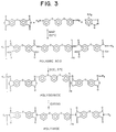
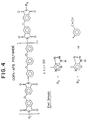
- Fig.3 illustrates the synthetic routes of ODPA-APB adhesive where R1 and R2 and n are defined in Fig. 4.
- Fig. 4 shows the ODPA-APB, polyimide chemical structure with 8-azaadenine and APA end groups.
- Fig. 5 displays TEM analysis of an adhesive and dielectric polyimide film adhered to a copper substrate in which the BPDA-PDA ([Bis(phenylenedicarboxylic acid) dianhydride-p-phenylene diamine ]) polyimide as well as the ODPA-APB (4,4'-oxydiphthalic anhydride-1,3-bis(aminophenoxy benzene) adhesive is free of copper oxide precipitates.
- BPDA-PDA [Bis(phenylenedicarboxylic acid) dianhydride-p-phenylene diamine ]
- ODPA-APB 4,4'-oxydiphthalic anhydride-1,3-bis(aminophenoxy benzene
- Adhesion between layers of polyimide and electrical circuit components such as integrated circuits, and means for forming electrical connections in an electrical circuit formed from conductive materials such as copper lines produced by a lithographic process or a wiring network within a ceramic or polymer substrate in electronic packaging is an important factor in obtaining the requisite reliability and longevity required in data processing equipment and related equipment.
- Various precursors of polyimides that can be employed in such an application comprise those based on PMDA-ODA polyamic acid, PMDA-ODA polyamic esters, BPDA-PDA polyamic esters, BPDA-PDA polyamic acid and THERMID as well as other polyimide precursors. None can fulfill all of the manufacturing requirements.
- the thick layers of PMDA-ODA build excessive stress during the curing stage i.e. when the polyamic acid solution applied to the substrate is converted to a polyimide at elevated temperatures. Additionally, it is difficult to obtain consistent adhesion values whereas PMDA-ODA and BPDA-PDA although having reasonably good properties have poor adhesion.
- THERMID has excellent adhesion properties, but less than desired mechanical properties and solvent resistance.
- a thin layer such as a layer anywhere from about 0.1 ⁇ m to about 5.0 ⁇ m of an acetylene or a vinyl terminated adhesive polyimide e.g. a THERMID or the adhesive polyimide described herein will avoid these problems.
- this adhesive polyimide when employed in thicknesses of from about 0.1 ⁇ m to about 5.0 ⁇ m and especially from about 0.3 ⁇ m to about 1.5 ⁇ m will have excellent adhesion, not only to other polyimides but also to metals and especially metals such as molybdenum, copper or nickel.
- the adhesive polyimide will prevent the formation of metal precipitates such as copper oxide or nickel oxide in the bulk polyimide film when the adhesive polyimide is employed either as the polyisoimide, polyimide or a polyamic ester based on an organic alcohol.
- the adhesive polyimide is being adhered to a metal substrate that will not react with polyamic acid to give metal precipitates such as a gold or chromium substrate or where the adhesive polyimide is being employed between two polyimide surfaces or between a polyimide surface and any other nonreactive non-metallic substrate, it may be employed in the polyamic acid form.
- any one of the adhesive polyimides described herein may be employed where polyimides are adhered to one another by means of the thin adhesive polyimide bonding layer or where polyimides are bonded to other non-metallic substrates such as ceramic substrates (e.g. glass ceramic) optionally having a wiring network embedded within the substrate, or to polymer, silicon or quartz substrates or substrates made from semiconductor materials such as gallium arsenide substrates, germanium substrates, the various art known equivalents thereof and the like.
- ceramic substrates e.g. glass ceramic
- substrates optionally having a wiring network embedded within the substrate, or to polymer, silicon or quartz substrates or substrates made from semiconductor materials such as gallium arsenide substrates, germanium substrates, the various art known equivalents thereof and the like.
- One of the essential features of the invention is in the discovery that the adhesive polyimide as described herein can be applied to a substrate as a relatively thin layer thereby taking advantage of its excellent adhesion properties followed by applying a relatively thick polyimide layer over it to take advantage of the superior electrical and mechanical properties of these polyimides.
- the problems encountered when employing thicker layers of the adhesive polyimides, such as poor mechanical properties, poor electrical properties and a tendency to craze as well as develop stress, are avoided.
- the poor adhesion properties of the polyimide are also avoided and advantage can be taken of their excellent electrical and mechanical properties.
- both the “adhesive polyimide” and the “polyimide” as broadly described herein are intended to include the polyisoimide, polyamic acid, polyamic ester of an alcohol having up to about 6 carbon atoms (and as defined herein) and the polyimide structure and are to be considered generic designations of these compounds unless otherwise indicated.
- polyimide may also comprise photosensitive polyimides (referred to hereafter as "PSPI") such as for example Ciba Geigy 412®, Asahi G6246A®, Toray 3840®, DuPont 2700® series, and the various art known equivalents thereof.
- PSPI compositions are further described by Higuchi et al . Chem. Mater. 1991, 3, 188-94 and Fyr et al ., U.S. Patent 4,551,552 and the various references cited in each, all of which are incorporated herein by reference.
- the process of the invention is especially useful in electronic packaging and especially multilevel packaging wherein metal conductors are provided in any one or several of the layers of the packaging structure.
- steps associated with chromium coating of metal conductors to improve adhesion both polymer-to-metal and metal-to-polymer types
- metal barrier layers can be eliminated altogether whether of the chromium or tantalum type or electroless metal type along with the multiple steps associated with electroless metallization such as palladium seeding, catalyst rinsing, post rinsing, post baking and the various complex bath controls and monitoring of the process to maintain bath quality.
- the process of the invention also eliminates additional surface treatments for polymer to polymer adhesion whether chemical roughening processes or plasma treating processes and/or the use of silane coupling agents. It should be noted, however, that when employing the process of the present invention that good adhesive bonding strengths will be obtained, if required, by using a plasma and/or silane coupling agent treatment step.
- silane coupling agents that may be employed in this regard include the following: trimethylchlorosilane dimethyldichlorosilane chloromethyldimethylchlorosilane N-trimethylsilyldiethylamine trimethylsilyliodide methylchlorosilanes octadecyltrichlorosilane octyl-phenyl-cyclohexyl-, or ethylsilanes (3,3,3 trifluororpropyl)trimethoxysilane [3-(2 aminoethyl)aminopropyl]trimethoxysilane cyanoethyltrimethoxysilane aminopropyltriethoxysilane aminopropyltrimethoxysilane phenyltrimethoxysilane (3-chloropropyl)trimethoxysilane (3-mercaptopropyl)trimethoxysilane (3-glycidoxypropyl
- the use of the adhesive polyimides according to the present invention will provide a continuous polymer adhesive coating over wiring surfaces and will further act to fill voids or gaps at the surface which is of particular importance for filling any separation between the polyimide layers and metal wiring sidewalls such as copper wiring sidewalls.
- the adhesive polyimide coating acts as a final planarizing layer in each layer in the multilevel packaging so that any surface irregularities in the layers will not be amplified as the packaging structure is built into a multi-level configuration.
- the invention also relates to a novel polymer having the structure R1 ⁇ I ⁇ n I-R2 wherein I is an imide group, isoimide group, amic acid group or an ester of said amic acid with an organo hydroxy compound having from one to about six carbon atoms, I being based on an aromatic diamine substituted completely or in part by an unsaturated heterocyclic diamine and/or a diamino organo phosphine and condensed with a cyclic tetracarboxylic acid anhydride.
- n is from about one to about 100 and especially from about 10 to about 30.
- R1 is a terminal unsaturated heterocyclic group or an organo phosphine group.
- the "imide” or “imido” moiety as set forth herein is intended to include any chemical group in which the three valence positions of the nitrogen atom of the group are filled or substituted by an atom or atoms other than hydrogen.
- the unsaturated heterocyclic group incorporated into the polymer backbone or polymer chain, and/or where it comprises the terminal unsaturated heterocyclic compound R1, contains nitrogen, oxygen or selenium, or any combination thereof as the hetero atoms in such group and is incorporated into said polymer (whether in the backbone and/or as a terminal group) through an imide group.
- R2 R1 or; wherein "Y" is previously defined; “b” is one or three.
- R1 may be an Benzyltriazole imide, 4-Pyrazolyl [3, 4-d]pyrimidine imide and 2-Purinyl imide, R1 may also be an: Imidazolyl; Pyrazolyl; Pyrazinyl; Pyrimidinyl; Pyridazinyl Indazoyl; Purinyl; Phthalazinyl; Naphthyridinyl; Quinoxalinyl; Quinazolinyl; 1,2,3-Triazolyl; 1,2,4-Triazolyl Thiazolyl; Isothiazolyl 1,3,5-Triazinyl; 1,2,4-Triazinyl; 1,2,3-Triazinyl; Pyrido[3,4-b]-pyridinyl; Pyrido[3,2-b]-pyridinyl; Pyrido[4,3-b]pyridinyl; Purinyl; Cinnolinyl; Pteridin
- radical R1 examples include: 2-Aminobenzimidazole; 4-Amino-2,1,3-benzothiadiazole; 2-Aminobenzothiazole; 2-Aminoimidazole; 5-Aminoindazole; 6-Aminoindazole; 4-Amino-6-mercaptopyrazolo[3,4-d]pyrimidine; 4-amino-2-mercaptopyrimidine; 3-Amino-5-mercapto-1,2,4-triazole; 2-Amino-4-methylpyrimidine; 2-Amino-5-methyl-1,3,4-thiadiazole; 2-Amino-4-methylthiazole; 3-amino-5-methylthio-1H-1,2,4-triazole; 2-Amino-4-phenylthiazole; 2-Amino-6-purinethiol; 3-Amino-4-pyrazolecarbonitrile; 2,4-Diamino-6-mercaptopyrimidine; 1,2,3-Triazole
- the unsaturated heterocyclic compound is incorporated in the polymer chain or backbone and is a part of the group "I" in the formula: This is done, for example, by substituting an unsaturated heterocyclic diamine for the aromatic diamine used in the synthesis of the polyimide.
- an unsaturated heterocyclic diamine for the aromatic diamine used in the synthesis of the polyimide.
- the aromatic diamine is substituted by the heterocyclic diamines in preparing the polyimide, anywhere from about 2 to about 100% of the aromatic diamines may be so substituted and especially from about 20% to about 100%.
- the following diamines may also be used: 3,5-Diamino-1,2,4-triazole; 2,6-Diaminopurine; 2,6-Diamino-8-purinol; 2,3-Diaminopyridine; These unsaturated heterocyclic diamines may also be produced by reducing: 2-Amino-6-nitrobenzothiazole; 2-Amino-5-(4-nitrophenylsulfonyl)thiazole; 2-Amino-5-nitropyrimidine; 2-Amino-5-nitrothiazole; 3-Amino-4-pyrazole carbonitrile; or by aminating with ammonia: 2-Amino-5-bromopyrimidine; 2-Amino-5-bromothiazole; 2-Amino-4-chlorobenzothiazole; 2-Amino-6-chlorobenzothiazole; 2-Amino-4-(4-chlorophenyl)thiazole; 2-Amino-6-chloropurine; 2-amino-6-fluorobenzothi
- Monoamines of these tricyclic compounds can also be similarly prepared where these tricyclics are to be in corporated as terminal groups on the polymer chain. These reactions of unsubstituted heterocyclic compounds with sodium amide and the like to form amine substitutes are further described by March, Advanced Organic Chemistry ( supra ) pp. 608-609.
- Selenium heterocyclic compounds corresponding to the foregoing sulfur heterocyclic compounds can also be employed, these selenium compounds being prepared in the same way as the sulfur compounds except that selenium based starting materials are employed in lieu of the sulfur starting materials, the preparation of such selenium heterocyclic compounds being known to a person with ordinary skill in the art. In selecting any of the foregoing unsaturated heterocyclic compounds for use in electronic packaging applications, those having relatively higher melting points are preferred.
- sulfur or selenium heterocyclics or sulfur or selenium substituted heterocyclics are preferred, and especially those containing sulfur.
- organo amino phosphines examples include 2-Aminoethyl phosphine; Tris(p-aminophenyl) phosphine; Bis(2-aminoehtyl)phenyl phosphine or Tris(2-aminoethyl)phosphine.
- This novel polymer comprises an adhesive polyimide which can be utilized in the article of manufacture or the process described herein.
- the heterocyclic group of this novel polymer provides the requisite terminal unsaturation.
- the foregoing adhesive polyimides comprising a polyamic acid can be converted into a polyamic acid ester by reacting the polyamic acid with an organohydroxy compound containing from 1 to about 6 carbon atoms whether an aliphatic, acyl or aromatic compound by combining a solution of the organohydroxy compound and the polyamic acid and heating mildly under a slight vacuum or in the presence of a mild dehydrating agent and the ester separated by conventional means.
- the adhesive polyimide in the form of the polyamic ester or polyisoimide may also be converted into a polyimide by heating at 250-400°C for about 1 to about 2 hours by thermal, microwave or infrared heating.
- the terminal unsaturated heterocyclic group is provided by employing as an anhydride or an amine, compounds such 8-Azaadenine (8-Aza-6-amino purine), Aminobenzotriazoles, Aminopurines such as 2-Aminopurine and Aminopyrazolopyrimidines such as 4-Amino pyrazolo[3,4-d] pyrimidine; 1,2,3-Triazole-4,5-dicarboxylic acid anhydride and the art known equivalents thereof.
- part of the terminal unsaturation may be provided by employing as part of the amine reactants an aminophenyl acetylene or other amino acetylene compounds and/or an aminostyrene or aminovinyl compounds.
- a mixture of any of the foregoing amines or anhydrides employed to provide unsaturation in the polymer can be used.
- THERMID 6000, 6015 and 6030 used in this and the other examples herein correspond to 0, 10, 15 and 30 repeat units n in formula 3 of Araps et al., U.S. 4,871,619, respectively.
- the polyimide thicknesses given is dry thickness and is described in this manner for all other examples herein.
- the polyimides employed in this and the other examples had a molecular weight of about 30,000 to about 40,000.
- THERMID 6015 was spin-coated onto a 9 ⁇ m-thick cured PMDA-ODA polyimide and then cured at 400°C for 1h to give 2 ⁇ m thickness of THERMID.
- the PMDA-ODA polyimide was previously coated onto a silicon wafer.
- the wafers thus prepared were tested for solvent crazing in both NMP (N-methylpyrrolidinone) and xylene by subjecting them to ultrasonic vibration at 85°C for 1h.
- An Ultrasonik (trademark) 300 ultrasona from the J.M. NEY Company was employed at 50-60Hz.
- the THERMID and PMDA-ODA polyimides did not craze and the adhesion between THERMID and polyimide was acceptable. Peel strengths could not be obtained since cohesive failure of polyimide is greater than peel strength.
- the combination of the adhesive and polyimide layers can be employed as dielectric layers for a serial packaging process as shown in Figure 1 which comprises a multilayer device 10 having a glass ceramic substrate 12 to which a silane coupling agent 14 is applied followed by an optional adhesive layer 16 and a polyimide layer 18 comprising a dielectric polyimide such as PMDA-ODA, BPDA-PDA and PSPI's.
- a metal conductor such as copper is employed.
- the adhesive polyimide in this invention gives good adhesion to copper while it does not react with copper.
- an adhesive metal such as chromium can be employed to enhance adhesion of copper to the polymer layer 18.
- all the adhesive layers, 16 and 20 are from about 0.1 ⁇ m to about 5 ⁇ m in thickness whereas the dielectric layers 18 and 22 are from about 5 ⁇ m to about 20 ⁇ m in thickness.
- the silane coupling agent applied as layer 14 is optional, it being discovered according to the present invention that excellent adhesion to the substrate can be obtained with the adhesive polyimide layers of the present invention at the thicknesses stated above.
- a 0.1% aqueous solution of a silane coupling agent was applied onto a glass ceramic substrate and baked. The dried coating was subsequently coated with a 20% by weight solution of THERMID 6015 in NMP solvent; and B-cured at 230°C for 30 min.
- a coating of 1-2 ⁇ m THERMID 6015 was applied to a silane coupling agent coated quartz wafer followed by curing at 400°C for forty minutes.
- a PMDA-ODA polyimide precursor solution was spin coated onto the THERMID and fully cured as described in Example 2 to give 20 ⁇ m thickness. It was determined that the 90° peel strength for PMDA-ODA to THERMID adhesion was 68g/mm.
- the THERMID 6015 after during, was down-streamed ashed with Plasmatech plasma equipment using oxygen and nitroso oxide gases followed by spin coating a non-acid precursor of PMDA-ODA polyimide at a thickness of 20 ⁇ m onto the THERMID.
- the 90° peel strength for THERMID-quartz substrate adhesion was 79g/mm. It was also determined that by applying a silane coupling agent to the surface of the THERMID after down-stream ashing the polyimide-THERMID peel strength was greater than 105g/mm.
- the molecular weight of the adhesive polyimide is low, it will fill any pinholes that are formed in the substrate and further has the advantage that planarization of each layer in a multilayer packaging arrangement may be improved by the application of the adhesive polyimide film such as the THERMID or other adhesive polyimide of the present invention to the substrate followed by the application of the polyimide.
- a subsequent dielectric layer of a photosensitive polyimide may be applied over the adhesive polyimide followed by exposing the photosensitive polyimide layer and developing it to form a via in the photosensitive layer.
- the via may be extended downwardly through the adhesive polyimide to the metal surface by a subsequent reactive ion etch (RIE) or by means of a plasma, wet etching with an alkaline material such as an alkali hydroxide or an amine or lastly by means of a laser to expose the metal surface in order to apply an electrical contact to the metal in the area where the via is formed.
- RIE reactive ion etch
- the glass ceramic substrate previously described was similarly ashed by means of an oxygen plasma and a silane coupling agent applied which was baked at 85°C for thirty minutes after which a thin layer of THERMID 6015 (between 0.1-2 ⁇ m) was coated onto the silylated layer and baked at 230°C for thirty minutes.
- An 18 ⁇ m thick layer of a polyimide film was deposited on the THERMID by dissolving a polyamic acid based on BPDA-PDA in NMP solvent and spin-coated onto the THERMID followed by baking at 150°C for thirty minutes, 230°C for thirty minutes, 300°C for 30 minutes and 400°C for 60 minutes.
- the peel strength was measured employing a 90° peel test and peel strengths of 120g/mm or greater were obtained between the THERMID and the substrate.
- peel strengths 120g/mm or greater were obtained between the THERMID and the substrate.
- a lower molecular weight BPDA-PDA polyimide was employed the peel layer could hot be peeled without breaking as evaluated when using a 90° peel test.
- Other types of THERMIDs can also be used such as 6000, 6010 and 6030 and substantially the same results obtained.
- an adhesive polyimide film as defined herein When applying an adhesive polyimide film as defined herein to a substrate that will react with polyamic acid such as a copper or a nickel substrate to form precipitates such as the oxides of copper or nickel in the polyimide film, it is important to utilize this polyimide precursor either in the isoimide, ester or imide form where the precipitates interfere with the electrical or physical properties of the article thus produced. Where the precipitates do not present such a problem, the polyamic acid form of the adhesive polyimide can be employed.
- samples of copper laminated to KAPTON (trademark) polyimide substrates were prepared, some of which were not treated prior to the application of THERMID 6015 while others were subjected to a ten minute 1M KOH hydrolysis at 55°C followed by a dilute acetic acid rinse.
- the hydrolysis process gives excellent THERMID-to-KAPTON polyimide and cleans off the copper oxides from the copper surface.
- THERMID 6015 A solution of THERMID 6015 was applied and cured at 250°C for one hour.
- THERMID films ranging in thickness from 0.3 ⁇ m to 5 ⁇ m were thus prepared and a thick coat of a PMDA-ODA polyimide as a peel layer was applied and cured to 400°C to give 20 ⁇ m thickness.
- the polymer-copper adhesion was measured using a standard 90° peel test method and was determined to be between about 30 to about 50g/mm for the various samples with no apparent dependence on the thickness of the THERMID or the type of pretreatment of the copper.
- Transmission Electron Microscopy (hereafter, "TEM") analysis of cross-section samples with about 0.3 ⁇ m THERMID show no reaction at the copper polymer interface and no diffusion of precipitates e.g. CuO into the polymer as illustrated in Figs. 2a and 2b.
- TEM Transmission Electron Microscopy
- Films as thin as about 0.3 ⁇ m or less provide not only an effective reaction barrier but also a good adhesive layer between the copper and the polyamic acid. This is also the case where there is no copper surface pretreatment.
- Fig. 2a is a TEM in cross-section of an article of manufacture 110 comprising a copper substrate 112 having a THERMID 6015 coating 114 applied to the copper surface which was neither pretreated with an alkaline material nor followed by an acid rinse.
- the coating 114 is about 0.2 ⁇ m thick.
- a subsequent PMDA-ODA polyamic acid coating 116 when applied as described above at a thickness of 20 ⁇ m does not show any precipitates such as copper oxide. This is in contrast to the copper oxide precipitates obtained when copper is coated with a polyamic acid as discussed and illustrated in Kim, et al . supra .
- Fig. 2b illustrates an article of manufacture 210 wherein a copper substrate 212 is pretreated with a caustic material followed by an acid rinse and then a 0.15 ⁇ m coating 214 of THERMID 6015 applied which in turn is coated with a layer 216 of PMDA-ODA as described above.
- a copper substrate 212 is pretreated with a caustic material followed by an acid rinse and then a 0.15 ⁇ m coating 214 of THERMID 6015 applied which in turn is coated with a layer 216 of PMDA-ODA as described above.
- no precipitates such as CuO were observed in the polyimide film (whether the THERMID or the PMDA-ODA polyimide) in contrast to polyamic acid solutions applied to copper substrates, again as described and illustrated by Kim et al . supra .
- a novel terminally unsaturated adhesive polyimide which comprises the condensation product of a dianhydride, a flexible diamine, an unsaturated heterocyclic monoamine and optionally a heterocyclic anhydride compound, an aminoacetylene compound and/or an aminovinyl compound.
- the unsaturated heterocyclic amino or anhydride compound and where used, the amino acetylene or amino vinyl compound will form end groups on the polyimide and have a tendency to complex with metals such as copper and the like to improve polymer-metal e.g. polymer-copper adhesion.
- Typical unsaturated heterocyclic monoamines have been described herein as well as the amino-phenylacetylenes, the aminoacetylenes or as an alternative, the aminostryrenes as well as the aminovinyl compounds, such as allylamine, all of which will improve the mechanical properties of the adhesive polymer by cross-linking in the curing stage of the polymer either with another acetylene group or vinyl group, as the case may be, or any carbonyl group contained within the polyimide.
- This cross-linking comprises an addition type of polymerization, and can generate 3-dimensional polymer networks in the cured polyimide.
- Conventional linear polyamic acid resins undergo only imidization upon heating and normally result in 2-dimensional networks.
- These unsaturated heterocyclic compound adhesion promoting groups are thermally stable (up to 400°C) and accordingly neither significant weight loss of polymer nor decomposition up to about 400°C is expected.
- novel adhesive polyimides are preferably prepared in the polyisoimide configuration although the polyamic acid, polyamic ester with an organic hydroxy compound containing up to about 6 carbon atoms or the polyimide may be prepared by processes known in the art.
- a solution of BTDA in anhydrous N-methylpyrrolidinone (NMP) is transferred to a flask which contains a solution of one equivalent of APB and 0.1-2 equivalents of the heterocyclic monoamine e.g. 8-azaadenine.
- NMP N-methylpyrrolidinone
- 0.1 equivalent of the end group will give 30 repeat units whereas two equivalents will yield one repeat unit.
- the addition of the end capping compounds which comprise the unsaturated heterocyclic nitrogen monoamines controls the molecular weight.
- the BTDA, APB and 8-Azaadenine (8-Aza-6-aminopurine) are reacted at 22°C in NMP for 24 hours to produce a polyamic acid which is converted to the polyisoimide by reaction with N-N '-dicyclohexylcarbodiimide (hereafter "DCC") at 5-20°C for a period of time from about 1 to about 24 hours.
- DCC N-N '-dicyclohexylcarbodiimide
- the polyisoimide product can be purified by recrystallization.
- Other dianhydrides and diamines such as BPDA, ODPA, PMDA, PDA and ODA can be used if different or improved mechanical properties are required.
- Example 7 Substantially the same procedures are followed as in Example 7 where 4,4'-oxydiphthalic anhydride ODPA ) and APB are employed so that polymers are obtained as shown in Figure 3.
- Figure 3 describes three step reactions which consist of a condensation reaction to yield polyamic acid, dehydration reaction to give polyisoimide and curing to polyimide.
- the condensation reaction is a typical synthetic method of producing polyamic acid.
- the dehydration reaction using DCC gives a polyisoimide which is soluble in NMP. This solution is employed in Examples 9 and 10.
- the polyisoimide product contains some amount of polyimide, but the polyimide does not hinder the application of polyisoimide.
- the polymer consisting of 4,4'-oxydiphthalic anhydride (ODPA), APB and nitrogen-containing end groups such as 8-azaadenine will be thermally stable since there are no unstable functional groups such as BTDA which cross-links at high temperature.
- ODPA 4,4'-oxydiphthalic anhydride
- APB 4,4'-oxydiphthalic anhydride
- nitrogen-containing end groups such as 8-azaadenine
- Polyamic acid and polyisoimide products can be purified by recrystallization using ethanol or isopropanol followed by washing with a solvent such as ether and drying. Both polyamic acid and polyisoimide can be cured to polyimide. Thermal, microwave or infrared curing can be employed.
- the ODPA-APB polyimide consists of thermally stable and flexible units as well as heterocyclic end groups, the flexible repeat units and end groups induce polymer-polymer interdiffusion and possible formation of polymer-copper complexes; thus polymer-polymer and polymer-copper adhesion is good.
- Another advantage is improvement of polyimide-polyimide adhesion especially in the case of microwave curing.
- ODPA-APB polyisoimide with 50% APA (aminophenylacetylene) and 50% 8-azaadenine end groups was synthesized.
- the approximate degree of polymerization is 30 and the polyimide cured at 400°C is thermally stable at 400°C.
- the weight loss is around 0.2%/hr at 400°C.
- This polymer was dissolved in NMP for spin-coating.
- a BPDA-PDA [Bis(phenylene dicarboxylic acid) dianhydride-p-Phenylene diamine] polyimide was coated onto a quartz wafer and cured. Both Cr (20 nm (200 ⁇ )) and Cu (2 ⁇ m) were coated on to the BPDA-PDA (on Quartz).
- the ODPA-APB-APA-8-azaadenine polymer was spin-coated onto the Cu followed by coating with the BPDA-PDA polyimide and then curing the whole polymer layer.
- the thickness of the ODPA-APB and BPDA-PDA are 2 ⁇ m and 15 ⁇ m after curing, respectively.
- the whole polymer layer was peeled at the copper polymer interface to give 52-64 g/mm (the peel rate was 1.5 mm/min) which is very good adhesion strength.
- Figure 5 is a TEM picture in cross-section of an article of manufacture 310 comprising a copper substrate 312 having an ODPA-APB-APA-8-azaadenine polymer coating 314 applied to the copper surface which was treated with acetic acid.
- a subsequent BPDA-PDA coating 316 was applied as described above at a thickness of 15 ⁇ m.
- An ODPA-APB polyisoimide with APA (aminophenylacetylene) end groups was prepared.
- the approximate degree of polymerization is 30 and the polyimide cured at 400°C is thermally stable at 400°C.
- the weight loss is around 0.2%/hr at 400°C.
- This polymer dissolved in NMP was spin-coated onto BPDA-PDA (20 ⁇ m) and cured.
- This film (2 ⁇ m ODPA-APB-APA and 20 ⁇ m BPDA-PDA after curing) was employed in a lamination experiment.
- BPDA-PDA polyimide was coated onto a Quartz wafer and cured.
- the face of the film of ODPA-APB-APA backed by BPDA-PDA was laminated onto Au/Cu/Cr backed by BPDA-PDA polyimide and a quartz wafer under 6.895 x 10⁵ N/m2 (100 psi) at 375°C for 1 hr.
- This lamination provided 50-60 g/mm peel strength at the Au-polymer interface (the peel rate was 1.5 mm/min) which is very good adhesion.
- a solution of BTDA in anhydrous NMP was cannulated into a flask which contained a solution of 1 equivalent of 3,5-diamino-1,2,4-triazole(TADA). The mixture was stirred for 24 h. The reaction gave BTDA-TADA polyamic acid which was cured to BTDA-TADA polyimide by heating.
- the infrared(IR)spectrum of the BTDA-TADA polyimide obtained comprise the following IR bands: 1792(m), 1738(vs), 1674(m), 1561(m),1514(m), 1458(m), 1426(w), 1391(m), 1348(s), 1291(m), 1244(s), 1181(w), 1156(w), 1096(m), 1042(w), cm ⁇ 1.
- the peaks at 1792, 1738 and 1348 cm ⁇ 1 correspond to typical imide carbonyl and C-N stretchings.
- the new polyimide eliminates the need for a metal (usually chromium) adhesive layer used with Cu conductors and thus simplifies the manufacturing process.
- metal usually chromium
- copper atoms form complexes with nitrogen-containing aromatic heterocyclic repeat units since copper has good reactivity with nitrogen-rich aromatic compounds. This chemical reaction provides good adhesion of copper onto the new polyimide, as has been demonstrated for Cu evaporated onto the surface.
Landscapes
- Chemical & Material Sciences (AREA)
- Chemical Kinetics & Catalysis (AREA)
- Health & Medical Sciences (AREA)
- Medicinal Chemistry (AREA)
- Polymers & Plastics (AREA)
- Organic Chemistry (AREA)
- Physics & Mathematics (AREA)
- Spectroscopy & Molecular Physics (AREA)
- Laminated Bodies (AREA)
- Macromolecular Compounds Obtained By Forming Nitrogen-Containing Linkages In General (AREA)
- Adhesives Or Adhesive Processes (AREA)
- Production Of Multi-Layered Print Wiring Board (AREA)
- Die Bonding (AREA)
Applications Claiming Priority (2)
| Application Number | Priority Date | Filing Date | Title |
|---|---|---|---|
| US771929 | 1991-10-07 | ||
| US07/771,929 US5326643A (en) | 1991-10-07 | 1991-10-07 | Adhesive layer in multi-level packaging and organic material as a metal diffusion barrier |
Publications (2)
| Publication Number | Publication Date |
|---|---|
| EP0536606A2 true EP0536606A2 (de) | 1993-04-14 |
| EP0536606A3 EP0536606A3 (en) | 1993-10-13 |
Family
ID=25093368
Family Applications (1)
| Application Number | Title | Priority Date | Filing Date |
|---|---|---|---|
| EP19920116437 Withdrawn EP0536606A3 (en) | 1991-10-07 | 1992-09-25 | An adhesive layer in multilevel packaging and organic material as a metal diffusion barrier |
Country Status (3)
| Country | Link |
|---|---|
| US (4) | US5326643A (de) |
| EP (1) | EP0536606A3 (de) |
| JP (1) | JP2817130B2 (de) |
Families Citing this family (92)
| Publication number | Priority date | Publication date | Assignee | Title |
|---|---|---|---|---|
| US5917707A (en) | 1993-11-16 | 1999-06-29 | Formfactor, Inc. | Flexible contact structure with an electrically conductive shell |
| US5231751A (en) * | 1991-10-29 | 1993-08-03 | International Business Machines Corporation | Process for thin film interconnect |
| US20020053734A1 (en) | 1993-11-16 | 2002-05-09 | Formfactor, Inc. | Probe card assembly and kit, and methods of making same |
| US5820014A (en) | 1993-11-16 | 1998-10-13 | Form Factor, Inc. | Solder preforms |
| US7073254B2 (en) | 1993-11-16 | 2006-07-11 | Formfactor, Inc. | Method for mounting a plurality of spring contact elements |
| US5391397A (en) * | 1994-04-05 | 1995-02-21 | Motorola, Inc. | Method of adhesion to a polyimide surface by formation of covalent bonds |
| JPH09116273A (ja) * | 1995-08-11 | 1997-05-02 | Shinko Electric Ind Co Ltd | 多層回路基板及びその製造方法 |
| US8033838B2 (en) | 1996-02-21 | 2011-10-11 | Formfactor, Inc. | Microelectronic contact structure |
| US5994152A (en) | 1996-02-21 | 1999-11-30 | Formfactor, Inc. | Fabricating interconnects and tips using sacrificial substrates |
| US5807660A (en) * | 1997-02-03 | 1998-09-15 | Taiwan Semiconductor Manufacturing Company Ltd. | Avoid photoresist lifting by post-oxide-dep plasma treatment |
| US6262478B1 (en) * | 1997-04-08 | 2001-07-17 | Amitec-Advanced Multilayer Interconnect Technologies Ltd. | Electronic interconnect structure and method for manufacturing it |
| US6141870A (en) | 1997-08-04 | 2000-11-07 | Peter K. Trzyna | Method for making electrical device |
| US20030129379A1 (en) * | 1999-04-23 | 2003-07-10 | Shigeru Yao | Porous insulating film and its laminates |
| JP3494098B2 (ja) * | 1999-12-20 | 2004-02-03 | ソニーケミカル株式会社 | フレキシブルプリント基板 |
| US7122900B2 (en) * | 2000-06-26 | 2006-10-17 | Renesas Technology Corp. | Semiconductor device and method manufacturing the same |
| US6627477B1 (en) | 2000-09-07 | 2003-09-30 | International Business Machines Corporation | Method of assembling a plurality of semiconductor devices having different thickness |
| EP1364424A2 (de) * | 2000-09-14 | 2003-11-26 | Fraunhofer-Gesellschaft zur Förderung der angewandten Forschung e.V. | Elektrochemisch aktivierbare schicht oder folie |
| US7334326B1 (en) | 2001-06-19 | 2008-02-26 | Amkor Technology, Inc. | Method for making an integrated circuit substrate having embedded passive components |
| US6930256B1 (en) | 2002-05-01 | 2005-08-16 | Amkor Technology, Inc. | Integrated circuit substrate having laser-embedded conductive patterns and method therefor |
| US7633765B1 (en) | 2004-03-23 | 2009-12-15 | Amkor Technology, Inc. | Semiconductor package including a top-surface metal layer for implementing circuit features |
| US7670962B2 (en) | 2002-05-01 | 2010-03-02 | Amkor Technology, Inc. | Substrate having stiffener fabrication method |
| US7548430B1 (en) | 2002-05-01 | 2009-06-16 | Amkor Technology, Inc. | Buildup dielectric and metallization process and semiconductor package |
| US6930257B1 (en) * | 2002-05-01 | 2005-08-16 | Amkor Technology, Inc. | Integrated circuit substrate having laminated laser-embedded circuit layers |
| US7399661B2 (en) | 2002-05-01 | 2008-07-15 | Amkor Technology, Inc. | Method for making an integrated circuit substrate having embedded back-side access conductors and vias |
| US9691635B1 (en) | 2002-05-01 | 2017-06-27 | Amkor Technology, Inc. | Buildup dielectric layer having metallization pattern semiconductor package fabrication method |
| US7569497B2 (en) * | 2002-07-30 | 2009-08-04 | Tokyo Electron Limited | Method and apparatus for forming insulating layer |
| US6641899B1 (en) * | 2002-11-05 | 2003-11-04 | International Business Machines Corporation | Nonlithographic method to produce masks by selective reaction, articles produced, and composition for same |
| DE10312815A1 (de) * | 2003-03-22 | 2004-10-07 | Henkel Kgaa | Verfahren zum Kontaminationstoleranten Kleben von Fügeteilen |
| US11081370B2 (en) | 2004-03-23 | 2021-08-03 | Amkor Technology Singapore Holding Pte. Ltd. | Methods of manufacturing an encapsulated semiconductor device |
| US10811277B2 (en) | 2004-03-23 | 2020-10-20 | Amkor Technology, Inc. | Encapsulated semiconductor package |
| US7145238B1 (en) | 2004-05-05 | 2006-12-05 | Amkor Technology, Inc. | Semiconductor package and substrate having multi-level vias |
| US20050276911A1 (en) * | 2004-06-15 | 2005-12-15 | Qiong Chen | Printing of organometallic compounds to form conductive traces |
| US8826531B1 (en) | 2005-04-05 | 2014-09-09 | Amkor Technology, Inc. | Method for making an integrated circuit substrate having laminated laser-embedded circuit layers |
| JP5079306B2 (ja) * | 2006-11-06 | 2012-11-21 | チェイル インダストリーズ インコーポレイテッド | 燃料電池用高分子電解質膜、膜−電極接合体及び燃料電池 |
| US20070195682A1 (en) | 2006-02-21 | 2007-08-23 | Duerig Urs T | Method for high density data storage and imaging |
| US8102753B2 (en) | 2006-02-21 | 2012-01-24 | International Business Machines Corporation | Method for forming deformed regions in a resin layer |
| JP5031824B2 (ja) * | 2006-05-03 | 2012-09-26 | デルファイ・テクノロジーズ・ホールディング・エス.アー.エール.エル. | アクチュエーターを被覆するための方法 |
| US20080076903A1 (en) * | 2006-08-31 | 2008-03-27 | Duerig Urs T | Data storage medium and method for high density data storage |
| US7589398B1 (en) | 2006-10-04 | 2009-09-15 | Amkor Technology, Inc. | Embedded metal features structure |
| US7550857B1 (en) | 2006-11-16 | 2009-06-23 | Amkor Technology, Inc. | Stacked redistribution layer (RDL) die assembly package |
| US7750250B1 (en) | 2006-12-22 | 2010-07-06 | Amkor Technology, Inc. | Blind via capture pad structure |
| US7752752B1 (en) | 2007-01-09 | 2010-07-13 | Amkor Technology, Inc. | Method of fabricating an embedded circuit pattern |
| US8323771B1 (en) | 2007-08-15 | 2012-12-04 | Amkor Technology, Inc. | Straight conductor blind via capture pad structure and fabrication method |
| KR101301349B1 (ko) * | 2009-01-06 | 2013-08-29 | 현대중공업 주식회사 | 동흡진기 |
| US8872329B1 (en) | 2009-01-09 | 2014-10-28 | Amkor Technology, Inc. | Extended landing pad substrate package structure and method |
| US7960827B1 (en) | 2009-04-09 | 2011-06-14 | Amkor Technology, Inc. | Thermal via heat spreader package and method |
| US8623753B1 (en) | 2009-05-28 | 2014-01-07 | Amkor Technology, Inc. | Stackable protruding via package and method |
| US8222538B1 (en) | 2009-06-12 | 2012-07-17 | Amkor Technology, Inc. | Stackable via package and method |
| US8471154B1 (en) | 2009-08-06 | 2013-06-25 | Amkor Technology, Inc. | Stackable variable height via package and method |
| US8796561B1 (en) | 2009-10-05 | 2014-08-05 | Amkor Technology, Inc. | Fan out build up substrate stackable package and method |
| US8937381B1 (en) | 2009-12-03 | 2015-01-20 | Amkor Technology, Inc. | Thin stackable package and method |
| US9691734B1 (en) | 2009-12-07 | 2017-06-27 | Amkor Technology, Inc. | Method of forming a plurality of electronic component packages |
| US8536462B1 (en) | 2010-01-22 | 2013-09-17 | Amkor Technology, Inc. | Flex circuit package and method |
| US8300423B1 (en) | 2010-05-25 | 2012-10-30 | Amkor Technology, Inc. | Stackable treated via package and method |
| US8294276B1 (en) | 2010-05-27 | 2012-10-23 | Amkor Technology, Inc. | Semiconductor device and fabricating method thereof |
| US8338229B1 (en) | 2010-07-30 | 2012-12-25 | Amkor Technology, Inc. | Stackable plasma cleaned via package and method |
| US8717775B1 (en) | 2010-08-02 | 2014-05-06 | Amkor Technology, Inc. | Fingerprint sensor package and method |
| US8337657B1 (en) | 2010-10-27 | 2012-12-25 | Amkor Technology, Inc. | Mechanical tape separation package and method |
| US8482134B1 (en) | 2010-11-01 | 2013-07-09 | Amkor Technology, Inc. | Stackable package and method |
| US9748154B1 (en) | 2010-11-04 | 2017-08-29 | Amkor Technology, Inc. | Wafer level fan out semiconductor device and manufacturing method thereof |
| US8525318B1 (en) | 2010-11-10 | 2013-09-03 | Amkor Technology, Inc. | Semiconductor device and fabricating method thereof |
| US8557629B1 (en) | 2010-12-03 | 2013-10-15 | Amkor Technology, Inc. | Semiconductor device having overlapped via apertures |
| US8535961B1 (en) | 2010-12-09 | 2013-09-17 | Amkor Technology, Inc. | Light emitting diode (LED) package and method |
| TWI617225B (zh) * | 2010-12-24 | 2018-03-01 | Lg伊諾特股份有限公司 | 印刷電路板及其製造方法 |
| TWI542264B (zh) * | 2010-12-24 | 2016-07-11 | Lg伊諾特股份有限公司 | 印刷電路板及其製造方法 |
| US9721872B1 (en) | 2011-02-18 | 2017-08-01 | Amkor Technology, Inc. | Methods and structures for increasing the allowable die size in TMV packages |
| US9013011B1 (en) | 2011-03-11 | 2015-04-21 | Amkor Technology, Inc. | Stacked and staggered die MEMS package and method |
| KR101140113B1 (ko) | 2011-04-26 | 2012-04-30 | 앰코 테크놀로지 코리아 주식회사 | 반도체 디바이스 |
| CN103732704A (zh) * | 2011-05-18 | 2014-04-16 | 户田工业株式会社 | 导电性涂膜的制造方法和导电性涂膜 |
| US8653674B1 (en) | 2011-09-15 | 2014-02-18 | Amkor Technology, Inc. | Electronic component package fabrication method and structure |
| US8633598B1 (en) | 2011-09-20 | 2014-01-21 | Amkor Technology, Inc. | Underfill contacting stacking balls package fabrication method and structure |
| US9029962B1 (en) | 2011-10-12 | 2015-05-12 | Amkor Technology, Inc. | Molded cavity substrate MEMS package fabrication method and structure |
| US8962890B1 (en) | 2012-04-20 | 2015-02-24 | The United States Of America As Represented By The Secretary Of The Air Force | Multifunctional crosslinkers for shape-memory polyimides, polyamides and poly(amide-imides) and methods of making the same |
| US8791227B1 (en) | 2012-04-20 | 2014-07-29 | The United States Of America As Represented By The Secretary Of The Air Force | Crosslinked aromatic polyimides and methods of making the same |
| KR20140048564A (ko) * | 2012-10-16 | 2014-04-24 | 삼성전기주식회사 | 코어기판, 그의 제조방법 및 메탈 비아용 구조체 |
| US9085661B1 (en) | 2012-10-26 | 2015-07-21 | The United States Of America As Represented By The Secretary Of The Air Force | Photomechanically active copolyimides derived from an azobenzenediamine, a rigid dianhydride, and a flexible dianhydride |
| KR101366461B1 (ko) | 2012-11-20 | 2014-02-26 | 앰코 테크놀로지 코리아 주식회사 | 반도체 디바이스 및 그 제조 방법 |
| US9799592B2 (en) | 2013-11-19 | 2017-10-24 | Amkor Technology, Inc. | Semicondutor device with through-silicon via-less deep wells |
| KR101488590B1 (ko) | 2013-03-29 | 2015-01-30 | 앰코 테크놀로지 코리아 주식회사 | 반도체 디바이스 및 그 제조 방법 |
| KR101607981B1 (ko) | 2013-11-04 | 2016-03-31 | 앰코 테크놀로지 코리아 주식회사 | 반도체 패키지용 인터포저 및 이의 제조 방법, 제조된 인터포저를 이용한 반도체 패키지 |
| US9139696B1 (en) | 2014-03-28 | 2015-09-22 | The United States Of America, As Represented By The Secretary Of The Air Force | Aromatic diamines containing three ether-linked-benzonitrile moieties, polymers thereof, and methods of making the same |
| US9644071B1 (en) | 2014-09-05 | 2017-05-09 | The United States Of America As Represented By The Secretary Of The Air Force | Bis(azobenzene) diamines and photomechanical polymers made therefrom |
| US9666514B2 (en) * | 2015-04-14 | 2017-05-30 | Invensas Corporation | High performance compliant substrate |
| US10239254B1 (en) | 2015-08-07 | 2019-03-26 | The United States Of America As Represented By The Secretary Of The Air Force | Method of fabricating shape memory films |
| US10294255B1 (en) | 2015-08-07 | 2019-05-21 | The United States Of America As Represented By The Secretary Of The Air Force | Multifunctional crosslinking agent, crosslinked polymer, and method of making same |
| US11065853B2 (en) * | 2016-04-28 | 2021-07-20 | Toyobo Co., Ltd. | Polyimide film layered body |
| US9960328B2 (en) | 2016-09-06 | 2018-05-01 | Amkor Technology, Inc. | Semiconductor device and manufacturing method thereof |
| JP7252020B2 (ja) | 2018-04-16 | 2023-04-04 | 旭化成株式会社 | ネガ型感光性樹脂組成物及び硬化レリーフパターンの製造方法 |
| JP7171890B2 (ja) * | 2019-03-15 | 2022-11-15 | 富士フイルム株式会社 | 硬化性樹脂組成物、硬化膜、積層体、硬化膜の製造方法、半導体デバイス、及び、ポリマー前駆体 |
| KR102903870B1 (ko) * | 2021-02-04 | 2025-12-23 | 주식회사 엘지화학 | 폴리이미드 수지 및 이를 포함하는 포지티브형 감광성 수지 조성물 |
| KR20230146065A (ko) * | 2021-03-16 | 2023-10-18 | 후지필름 가부시키가이샤 | 수지 조성물, 경화물, 적층체, 경화물의 제조 방법, 및, 반도체 디바이스 |
| JP2023157637A (ja) * | 2022-04-15 | 2023-10-26 | 河村産業株式会社 | 末端変性ポリイミド |
Family Cites Families (30)
| Publication number | Priority date | Publication date | Assignee | Title |
|---|---|---|---|---|
| US3361589A (en) * | 1964-10-05 | 1968-01-02 | Du Pont | Process for treating polyimide surface with basic compounds, and polyimide surface having thin layer of polyamide acid |
| US3770573A (en) * | 1971-06-08 | 1973-11-06 | Du Pont | Interdiffusionally bonded structures of polyimide polymeric material |
| US3791848A (en) * | 1972-05-19 | 1974-02-12 | Western Electric Co | A method of improving the adherence of a metal deposit to a polyimide surface |
| DE2462113C3 (de) * | 1973-04-03 | 1979-03-08 | Hughes Aircraft Co., Culver City, Calif. (V.St.A.) | Acetylensubstituierte Polyamid-Oligomere |
| JPS5811449B2 (ja) * | 1977-05-23 | 1983-03-03 | ヒュ−ズ・エアクラフト・カンパニ− | アセチレン置換ポリイミドオリゴマ−より硬化された樹脂を製造する方法 |
| US4543295A (en) * | 1980-09-22 | 1985-09-24 | The United States Of America As Represented By The Director Of The National Aeronautics And Space Administration | High temperature polyimide film laminates and process for preparation thereof |
| US4386116A (en) * | 1981-12-24 | 1983-05-31 | International Business Machines Corporation | Process for making multilayer integrated circuit substrate |
| JPS58157190A (ja) * | 1982-03-12 | 1983-09-19 | 日立化成工業株式会社 | フレキシブル印刷回路用基板の製造法 |
| US4667006A (en) * | 1983-06-20 | 1987-05-19 | Asahi Kasei Kogyo Kabushiki Kaisha | Poly(ethynylphenyl)acetylene, its copolymer and composition thereof |
| US4654223A (en) | 1983-11-30 | 1987-03-31 | International Business Machines Corporation | Method for forming a film of dielectric material on an electric component |
| US4749621A (en) * | 1983-11-30 | 1988-06-07 | International Business Machines Corporation | Electronic components comprising polyimide-filled isolation structures |
| US4699803A (en) * | 1983-11-30 | 1987-10-13 | International Business Machines Corporation | Method for forming electrical components comprising cured vinyl and/or acetylene terminated copolymers |
| US4871619A (en) * | 1983-11-30 | 1989-10-03 | International Business Machines Corporation | Electronic components comprising polymide dielectric layers |
| US4656050A (en) * | 1983-11-30 | 1987-04-07 | International Business Machines Corporation | Method of producing electronic components utilizing cured vinyl and/or acetylene terminated copolymers |
| US4551552A (en) * | 1984-05-23 | 1985-11-05 | E. I. Du Pont De Nemours And Company | Process for preparing rimantadine |
| DE3566483D1 (en) * | 1984-06-30 | 1988-12-29 | Akzo Gmbh | Flexible polyimide multilayer laminate |
| US4568601A (en) * | 1984-10-19 | 1986-02-04 | International Business Machines Corporation | Use of radiation sensitive polymerizable oligomers to produce polyimide negative resists and planarized dielectric components for semiconductor structures |
| US4835197A (en) * | 1985-01-04 | 1989-05-30 | Raychem Corporation | Aromatic polymer compositions |
| DE3506524A1 (de) * | 1985-02-25 | 1986-08-28 | Akzo Gmbh, 5600 Wuppertal | Flexible polyimid-mehrschichtlaminate |
| US4634631A (en) * | 1985-07-15 | 1987-01-06 | Rogers Corporation | Flexible circuit laminate and method of making the same |
| JPS6288346A (ja) * | 1985-10-15 | 1987-04-22 | Hitachi Ltd | 多層配線基板 |
| DE3684307D1 (de) * | 1985-10-31 | 1992-04-16 | Mitsui Toatsu Chemicals | Flexibles laminat fur platine fur gedruckte schaltkreise und verfahren zu seiner herstellung. |
| JPS62140822A (ja) * | 1985-12-17 | 1987-06-24 | Ube Ind Ltd | ポリイミド積層シ−トおよびその製造法 |
| US4784707A (en) * | 1986-02-07 | 1988-11-15 | Aluminum Company Of America | Method of making electrical connections using joint compound |
| US4885038A (en) * | 1986-05-01 | 1989-12-05 | International Business Machines Corporation | Method of making multilayered ceramic structures having an internal distribution of copper-based conductors |
| US4923718A (en) * | 1986-10-14 | 1990-05-08 | Takiron Co., Ltd. | Functional film and process for its production |
| US4775449A (en) * | 1986-12-29 | 1988-10-04 | General Electric Company | Treatment of a polyimide surface to improve the adhesion of metal deposited thereon |
| US4832808A (en) * | 1987-01-02 | 1989-05-23 | International Business Machines Corporation | Polyimides reaction products and use in electrophoretic deposition |
| US5104734A (en) * | 1988-06-03 | 1992-04-14 | International Business Machines Corporation | Method for improving adhesion between a polyimide layer and a metal and the article obtained |
| US4957661A (en) * | 1988-09-30 | 1990-09-18 | The United States Of America As Represented By The United States National Aeronautics And Space Administration | Graphite fluoride fiber polymer composite material |
-
1991
- 1991-10-07 US US07/771,929 patent/US5326643A/en not_active Expired - Fee Related
-
1992
- 1992-09-07 JP JP26425492A patent/JP2817130B2/ja not_active Expired - Lifetime
- 1992-09-25 EP EP19920116437 patent/EP0536606A3/en not_active Withdrawn
-
1994
- 1994-02-17 US US08/197,941 patent/US5569739A/en not_active Expired - Fee Related
-
1995
- 1995-06-07 US US08/475,412 patent/US5599582A/en not_active Expired - Fee Related
- 1995-06-07 US US08/474,985 patent/US5582858A/en not_active Expired - Fee Related
Also Published As
| Publication number | Publication date |
|---|---|
| EP0536606A3 (en) | 1993-10-13 |
| JPH06106678A (ja) | 1994-04-19 |
| JP2817130B2 (ja) | 1998-10-27 |
| US5599582A (en) | 1997-02-04 |
| US5569739A (en) | 1996-10-29 |
| US5326643A (en) | 1994-07-05 |
| US5582858A (en) | 1996-12-10 |
Similar Documents
| Publication | Publication Date | Title |
|---|---|---|
| US5599582A (en) | Adhesive layer in multi-level packaging and organic material as a metal diffusion barrier | |
| EP0456972B1 (de) | Modifizierung einer Polyimidoberfläche | |
| EP0133533B1 (de) | Harzmaterial mit geringer thermischer Ausdehnung für Verdrahtungsisolationsfolie | |
| JPS61111359A (ja) | ポリイミド膜 | |
| US5527621A (en) | Method for surface treatment of polyimide resin molded articles | |
| US6084053A (en) | Electronic part and process for manufacturing the same | |
| US5133989A (en) | Process for producing metal-polyimide composite article | |
| KR20110035620A (ko) | 폴리이미드 필름 | |
| EP0040415B1 (de) | Wärmebeständige Harzzusammensetzungen und ihre Verwendung zum Beschichten von Metallsubstraten | |
| Lee et al. | Formation of polyimide-Cu complexes: improvement of direct Cu-on-PI and PI-on-Cu adhesion | |
| JP3486012B2 (ja) | ポリイミドシロキサンブロック共重合体、それを含むワニスおよびその使用方法 | |
| EP0361462A2 (de) | Verfahren zur Herstellung eines aus Kupfer oder Silber/Polyimid zusammengesetzten Artikels | |
| US5063115A (en) | Electronic device coated with a polyimide coating composition | |
| EP0304022A2 (de) | Polyimid-Beschichtungsmaterial | |
| JP3079740B2 (ja) | ポリイミド及びそれを用いた配線構造体 | |
| EP0535444A1 (de) | Modifikationen von Polyimid zu Isoimid und Reaktion mit nukleophilen Agentien | |
| KR101475839B1 (ko) | 인쇄회로기판용 동박, 그 제조 방법 및 폴리아믹산전구체와 동박을 사용한 연성동박적층필름 | |
| JPH01319941A (ja) | ポリイミド層と金属の間の接着力を強化する方法 | |
| JPH02251584A (ja) | ヘテロ環含有ポリイミド複合体 | |
| KR100418545B1 (ko) | 폴리이미드 고내열 접착제 및 이를 이용한 접착테이프 | |
| JPH01222945A (ja) | フレキシブル金属箔積層材 | |
| JPH01174439A (ja) | フレキシブル金属箔積層材 | |
| TW202146232A (zh) | 金屬被覆聚合物膜及電子裝置 | |
| JPH0532891A (ja) | 熱硬化性樹脂組成物およびそれを用いたプリント配線板 | |
| KR100560109B1 (ko) | 폴리아미드산 및 폴리이미드의 제조방법 |
Legal Events
| Date | Code | Title | Description |
|---|---|---|---|
| PUAI | Public reference made under article 153(3) epc to a published international application that has entered the european phase |
Free format text: ORIGINAL CODE: 0009012 |
|
| AK | Designated contracting states |
Kind code of ref document: A2 Designated state(s): DE FR GB |
|
| PUAL | Search report despatched |
Free format text: ORIGINAL CODE: 0009013 |
|
| AK | Designated contracting states |
Kind code of ref document: A3 Designated state(s): DE FR GB |
|
| 17P | Request for examination filed |
Effective date: 19930819 |
|
| 17Q | First examination report despatched |
Effective date: 19951024 |
|
| 18D | Application deemed to be withdrawn |
Effective date: 19960902 |