EP0536687B1 - Verfahren und Einrichtung zur Demodulation mit adaptiver Phasenreglung bei pseudo-kohärenter Detektion - Google Patents
Verfahren und Einrichtung zur Demodulation mit adaptiver Phasenreglung bei pseudo-kohärenter Detektion Download PDFInfo
- Publication number
- EP0536687B1 EP0536687B1 EP92117020A EP92117020A EP0536687B1 EP 0536687 B1 EP0536687 B1 EP 0536687B1 EP 92117020 A EP92117020 A EP 92117020A EP 92117020 A EP92117020 A EP 92117020A EP 0536687 B1 EP0536687 B1 EP 0536687B1
- Authority
- EP
- European Patent Office
- Prior art keywords
- complex
- frequency error
- signals
- error
- input signals
- Prior art date
- Legal status (The legal status is an assumption and is not a legal conclusion. Google has not performed a legal analysis and makes no representation as to the accuracy of the status listed.)
- Expired - Lifetime
Links
Images








Classifications
-
- H—ELECTRICITY
- H04—ELECTRIC COMMUNICATION TECHNIQUE
- H04L—TRANSMISSION OF DIGITAL INFORMATION, e.g. TELEGRAPHIC COMMUNICATION
- H04L27/00—Modulated-carrier systems
- H04L27/18—Phase-modulated carrier systems, i.e. using phase-shift keying
- H04L27/22—Demodulator circuits; Receiver circuits
- H04L27/233—Demodulator circuits; Receiver circuits using non-coherent demodulation
- H04L27/2332—Demodulator circuits; Receiver circuits using non-coherent demodulation using a non-coherent carrier
-
- H—ELECTRICITY
- H04—ELECTRIC COMMUNICATION TECHNIQUE
- H04L—TRANSMISSION OF DIGITAL INFORMATION, e.g. TELEGRAPHIC COMMUNICATION
- H04L27/00—Modulated-carrier systems
- H04L27/0014—Carrier regulation
- H04L2027/0024—Carrier regulation at the receiver end
- H04L2027/0026—Correction of carrier offset
- H04L2027/003—Correction of carrier offset at baseband only
-
- H—ELECTRICITY
- H04—ELECTRIC COMMUNICATION TECHNIQUE
- H04L—TRANSMISSION OF DIGITAL INFORMATION, e.g. TELEGRAPHIC COMMUNICATION
- H04L27/00—Modulated-carrier systems
- H04L27/0014—Carrier regulation
- H04L2027/0044—Control loops for carrier regulation
- H04L2027/0046—Open loops
- H04L2027/0048—Frequency multiplication
Definitions
- the present invention relates to a quasi-coherent detection in which a quadrature detection of modulated input signals at a local oscillator frequency is made, and a phase compensation is made on baseband signals converted from the detected input signals.
- a conventional quasi-coherent detection circuit for the high speed data transmission is disclosed in Ohtani et al. "Development of Digital MODEM LSI for Satellite Communications", Electronic Information Communication Society, Satellite Communication Study Session SAT88-7, pp.39-45, which has a configuration shown in Fig. 1.
- This configuration of Fig. 1 is basically a conventionally known carrier recovery circuit configuration implemented in terms of baseband range digital signals.
- a signal line for a complex quantity is indicated by a thick line, while a signal line for a scalar quantity is indicated by a thin line.
- a carrier range complex multiplier 1 makes the quadrature detection of the modulated input signals S at a local frequency of a local oscillator 2, and after the noise components are removed by low pass filters 3, the detected input signals are converted into digital signals at A/D converters 4 and entered into a digital PLL (Phase Lock Loop) circuit 9.
- PLL Phase Lock Loop
- the phase rotation due to the frequency error is corrected at a digital complex multiplier 5. Then, the phase error is detected at a phase comparator 6, and the error voltage is integrated at a loop filter 7, so as to provide the feedback from a digital VCO (Voltage Controlled Oscillator) 8 to the digital complex multiplier 5.
- VCO Voltage Controlled Oscillator
- the acquisition time is determined by the time constant and the loop gain of the loop filter 7 which are the loop parameters of the digital PLL circuit 9.
- the quasi-coherent detection of modulated input signals S having N symbols for forming one burst is made by the carrier range complex multiplier 1, the local oscillator 2, the low pass filters 3, and the A/D converters 4, which are similar to those appeared in the circuit of Fig. 1 described above.
- the carrier recovery is achieved by the averaging process using the power multiplication operations and the least square algorithm, where the total error including the initial phase error and the frequency error is estimated by using the least square algorithm, and the phase rotation is corrected according to the result of this estimation at a phase rotation correction estimation unit 10 shown in detail in Fig. 3.
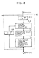
- the phase rotation correction estimation unit 10 shown in Fig. 3 when the modulated input signals S are the M-array phase shift keying modulation signals, the tentatively demodulated signals U obtained at the A/D converters 4 are temporarily stored in a memory unit 11 shown in Fig. 2. Meawhile, the modulation components are removed by multiplying the tentatively demodulated signals U for M times at an M-th power multiplication circuit 12-1. Then, the phase rotation is corrected at a digital complex multiplier 5-2 by calculating a complex multiplication of the beat components obtained by the M-th power multiplication circuit 12-1 and the correction signals for up to the immediately previous symbol multiplied for M times by another M-th power multiplication circuit 12-2.
- the least square estimation value for the immediately previous symbol is corrected by the newly obtained estimation value at an estimation value correction circuit 13.
- the tentatively demodulated signals U including the beat components which are stored in a memory circuit 11 are multiplied with the complex signals Z obtained by the phase rotation correction estimation unit 10 sequentially at a digital complex multiplier 5-1 to obtain the final demodulated signals.
- this block demodulation requires a memory circuit with a memory capacity equal to the length of the burst, as well as many complex multipliers and adders, so that the circuit size inevitably becomes quite large.
- a delay of at least one burst length is required in obtaining the final demodulated signals, so that it is not applicable to an application requiring the real time operation.
- Another example of a conventional quasi-coherent detection for the high speed data transmission is a method for estimating the phase of the carrier by using the linear estimation, disclosed in Sanpei, "QPSL Coherent Detection Method for Land Mobile Radio Communications Using Linear Mean Square Estimation", Electronic Information Communication Society B-II, Vol.J 72-B-II, No.4, pp.125-132.
- a method of demodulation with adaptive phase control for obtaining demodulated complex signals from modulated complex input signals, comprising the steps of: estimating a frequency error in the modulated complex input signals by using a phase variation during one symbol due to the frequency error according to the modulated complex input signals and the demodulated complex signals for present and immediately previous symbols; estimating an initial phase error in the modulated complex input signals, according to said modulated complex input signals, said demodulated complex signals and the estimated frequency error; and applying optimum phase compensation based on the estimated frequency error and the estimated initial phase error to said modulated complex input signals in order to obtain said demodulated complex signals.
- an apparatus for demodulation with adaptive phase control for obtaining demodulated complex signals from modulated complex input signals, comprising: means for estimating a frequency error in the modulated complex input signals by using a phase variation during one symbol due to the frequency error according to the modulated complex input signals and the demodulated complex signals for present and immediately previous symbols; means for estimating an initial phase error in the modulated complex input signals, according to said modulated complex input signals, said demodulated complex signals, and the estimated frequency error; and means for applying optimum phase compensation based on the estimated frequency error and the estimated initial phase error to said modulated complex input signals in order to obtain said demodulated complex signals.
- Fig. 1 is a block diagram of a first example of a conventional quasi-coherent detection circuit for the high speed transmission.
- Fig. 2 is a block diagram of a second example of a conventional quasi-coherent detection circuit for the high speed transmission.
- Fig. 3 is a detailed block diagram of a phase rotation correction estimation unit in the conventional quasi-coherent detection circuit shown in Fig. 2.
- Fig. 4 is a block diagram of a first embodiment of an apparatus for demodulation with adaptive phase control in quasi-coherent detection, according to the present invention.
- Fig. 5 is a detailed block diagram of a phase control circuit in the apparatus of Fig. 4.
- Fig. 6 is a detailed block diagram of a correlation value weighted accumulation circuit in the phase control circuit of Fig. 5.
- Fig. 7 is a detailed block diagram of an exponentially weighted accumulation circuit in the correlation value weighted accumulation circuit of Fig. 6.
- Fig. 8 is a detailed block diagram of a complex normalization circuit in the correlation value weighted accumulation circuit of Fig. 6.
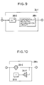
- Fig. 9 is a detailed block diagram of an auto correlation value weighted accumulation circuit in the phase control circuit of Fig. 5.
- FIg. 10 is a detailed block diagram of an exponentially weighted accumulation circuit in the auto correlation value weighted accumulation circuit of Fig. 9.
- Fig. 11 is a detailed block diagram of an involution circuit in the phase control circuit of Fig. 5.
- Fig. 12 is a detailed block diagram of a cross correlation value weighted accumulation circuit in the phase control circuit of Fig. 5.
- Fig. 13 is a detailed block diagram of a phase control circuit in a second embodiment of an apparatus for demodulation with adaptive phase control in quasi-coherent detection, according to the present invention.
- Fig. 14 is a detailed block diagram of a frequency error detection circuit in the phase control circuit of Fig. 13.
- Fig. 15 is a detailed block diagram of a phase error detection circuit in the phase control circuit of Fig. 13.
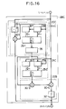
- Fig. 16 is a detailed block diagram of a phase control circuit in a third embodiment of an apparatus for demodulation with adaptive phase control in quasi-coherent detection, according to the present invention.
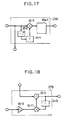
- Fig. 17 is a detailed block diagram of a correlation value weighted accumulation circuit in the phase control circuit of Fig. 16.
- Fig. 18 is a detailed block diagram of a cross correlation value weighted accumulation circuit in the phase control circuit of Fig. 16.
- Fig. 19 is a detailed block diagram of a frequency compensation circuit in a phase control circuit, in a fourth embodiment of an apparatus for demodulation with adaptive phase control in quasi-coherent detection, according to the present invention.
- Fig. 20 is a detailed block diagram of a frequency compensation circuit in a phase control circuit, in a fifth embodiment of an apparatus for demodulation with adaptive phase control in quasi-coherent detection, according to the present invention.
- a signal line for a complex quantity is indicated by a thick line, while a signal line for a scalar quantity is indicated by a thin line.
- This apparatus of Fig. 4 includes: a carrier range complex multiplier 1, a local oscillator 2, low pass filters 3, and A/D converters 4, which are similar to those used in the conventional quasi-coherent detection apparatus described above.
- the tentatively demodulated signals U in a form of a series of sampled values generated at symbol periods are then supplied to a phase control circuit 28 in which all the processings are carried out digitally.
- the phase control circuit 28 comprises: a phase error estimation circuit 21, a phase equalization circuit 22, a frequency compensation circuit 44, a training signal generation circuit 45, and a switching circuit 46, which realizes a Wiener filter as a whole.
- the frequency compensation circuit 44 further comprises: a phase variation estimation circuit 20 and an involution circuit 29, and functions to make an estimation for phase compensation required by a frequency error in the tentatively demodulated signals U.
- the phase variation estimation circuit 20 estimates the phase variation due to the frequency error by using RLS (Recursive Least Square) algorithm in the tentatively demodulated signals U entered from the A/D converters 4, and outputs the obtained phase variation estimation to the involution circuit 29.
- RLS Recursive Least Square
- the phase error estimation circuit 21 estimates the initial phase error due to the frequency error by using RLS (Recursive Least Square) algorithm in the tentatively demodulated signals U entered from the A/D converters 4, according to the output of the involution circuit 29.
- RLS Recursive Least Square
- the phase equalization circuit 22 makes the phase equalization in the tentatively demodulated signals U entered from the A/D converters 4, according to the outputs of the phase variation estimation circuit 20, the involution circuit 29, and the phase error estimation circuit 21, to obtain the demodulated complex signals D.
- the training signal generation circuit 45 generates the training signals to be used in the phase variation estimation circuit 20 and the phase error estimation circuit 21, and the switching circuit 46 selectively supplies either the training signals generated by the training signal generation circuit 45 or the demodulated complex signals D outputted by the phase equalization circuit 22 to the phase variation estimation circuit 20 and the phase error estimation circuit 21.
- the switching circuit 46 initially selects the training signals from the training signal generation circuit 45, and then subsequently switches to the demodulated complex signals D from the phase equalization circuit 22 later on. These training signal generation circuit 45 and the switching circuit 46 may be omitted if desired.
- the phase control circuit 28 has a configuration as shown in Fig. 5.
- the phase variation estimation circuit 20 in the frequency compensation circuit 44 further comprises: a complex conjugation circuit 26-1 for taking a complex conjugation of the tentatively demodulated signals U; a complex multiplier 30-1 for calculating a cross correlation value of the complex conjugate of the tentatively demodulated signals U obtained at the complex conjugation circuit 26-1 and the demodulated complex signals D outputted from the phase equalization circuit 22; a correlation value weighted accumulation circuit 23 to be described below; an auto correlation value weighted accumulation circuit 24-1 to be described below; and a divider 25-1 to be described below.
- the cross correlation value is taken at the complex multiplier 30-1 in order to remove the modulation components and leave the beat components in the tentatively demodulated signals U.
- the correlation value weighted accumulation circuit 23 in the phase variation estimation circuit 20 functions to normalize the correlation value obtained by the complex multiplier 30-1, detect the variation during one symbol, and calculate the accumulation value of the detected variations weighted by a forgetting factor ⁇ 1 , and has a detail configuration as shown in Fig. 6.
- the correlation value weighted accumulation circuit 23 comprises: a complex normalization circuit 35 for normalizing the correlation value obtained by the complex multiplier 30-1; a complex conjugation circuit 26-2 for taking a complex conjugate of the normalized correlation value obtained by the complex normalization circuit 35; a delay circuit 31-1 for delaying the complex conjugate obtained by the complex conjugation circuit 26-2 for one symbol period; a complex multiplier 30-5 for multiplying the normalized correlation value obtained by the complex normalization circuit 35 and the delayed complex conjugate outputted from the delay circuit 31-1, so as to obtain the variation during one symbol; and an exponentially weighted accumulation circuit 38a-1 for calculating the exponentially weighted accumulation value ⁇ ' n of the variations obtained by the complex multiplier 30-5.
- the normalized correlation value obtained by the complex normalization circuit 35 is also outputted to the auto correlation value weighted accumulation circuit 24-1, while the exponentially weighted accumulation value ⁇ ' n calculated by the exponentially weighted accumulation circuit 38a-1 is outputted to the divider 25-1.
- the exponentially weighted accumulation circuit 38a-1 further comprises, as shown in Fig. 7, an adder 33-1, a weight circuit 34-1 for weighting an output of the adder 33-1 with the forgetting factor ⁇ 1 , and a delay circuit 31-2 for delaying the weighted output obtained by the weight circuit 34-1 for one symbol period and supplying it to the adder 33-1 such that the adder 33-1 adds the output of the complex multiplier 30-5 and the delayed output supplied from the delay circuit 31-2.
- the complex normalization circuit 35 further comprises, as shown in Fig. 8, a complex square multiplication circuit 36-1 for calculating a complex square multiplication of the input denoted as A in Fig. 8, a square root circuit 37 for calculating a square root of the complex square multiplication calculated by the complex square multiplication circuit 36-1 which is denoted as B in Fig. 8, and a divider 25-3 for dividing the input A by the square root of the complex square multiplication B, so as to obtain the absolute value of the input A.
- the auto correlation value weighted accumulation circuit 24-1 in the phase variation estimation circuit 20 functions to calculate the accumulation value of the normalized correlation value supplied from the complex normalization circuit 35 weighted by a forgetting factor ⁇ 2 which may be equal to the forgetting factor ⁇ 1 , and has a detail configuration as shown in Fig. 9.
- the auto correlation value weighted accumulation circuit 24-1 comprises: a complex square multiplication circuit 36-2 for calculating a complex square multiplication of the normalized correlation value supplied from the complex normalization circuit 35; and an exponentially weighted accumulation circuit 38b for calculating the exponentially weighted accumulation value ⁇ ' n of the complex square multiplication obtained by the complex square multiplication circuit 36-2.
- the exponentially weighted accumulation value ⁇ ' n calculated by the exponentially weighted accumulation circuit 38b which is a scalar quantity, is outputted to the divider 25-1.
- the exponentially weighted accumulation circuit 38b further comprises, as shown in Fig. 10, an adder 33-2, a weight circuit 34-2 for weighting an output of the adder 33-2 with the forgetting factor ⁇ 2 , and a delay circuit 31-3 for delaying the weighted output obtained by the weight circuit 34-2 for one symbol period and supplying it to the adder 33-2 such that the adder 33-2 adds the output of the complex square multiplication circuit 36-2 and the delayed output supplied from the delay circuit 31-3.
- the divider 25-1 in the phase variation estimation circuit 20 divides the exponentially weighted accumulation value ⁇ ' n supplied from the correlation value weighted accumulation circuit 23 by the exponentially weighted accumulation value ⁇ ' n supplied from the auto correlation value weighted accumulation circuit 24-1.
- the output ⁇ ' n / ⁇ ' n obtained by the divider 25-1, which indicates the phase variation estimation, is then supplied to the involution circuit 29 as well as to the phase equalization circuit 22.
- the variation during one symbol obtained by the complex multiplier 30-5 in the correlation value weighted accumulation circuit 23 is proportional to the frequency error in the tentatively demodulated signals U for that one symbol, and the phase variation estimation obtained by the divide 25-1 indicates an ensemble average of the phase variations during one symbol in the tentatively demodulated signals U.
- the involution circuit 29 in the frequency compensation circuit 44 calculates the involution of the output ⁇ ' n / ⁇ ' n outputted by the divider 25-1 to obtain the total phase variation for the n-th symbol, which is taken as the estimation of phase compensation required by a frequency error, and has a detail configuration as shown in Fig. 11.
- the involution circuit comprises: a complex multiplier 30-6, a delay circuit 31-4 for delaying an output of the complex multiplier 30-6 for one symbol period such that the complex multiplier 30-6 multiplies the output ⁇ ' n / ⁇ ' n supplied from the divider 25-1 by itself, and a complex conjugation circuit 26-3 for taking the complex conjugate of the output of the complex multiplier 30-6 so as to obtain the involution.
- the involution obtained by the involution circuit 29, which indicates the estimation of phase compensation required by a frequency error, is then supplied to the phase error estimation circuit 21 as well as to the phase equalization circuit 22.
- the frequency error estimated by the frequency compensation circuit 44 does not account for the initial phase error.
- the phase variation can be caused by the Rayleigh fading, even when the frequency error is equal to zero.
- it is further necessary to make an estimation for the initial phase error in order to be able to compensate the phase variation due to such an initial phase error.
- the phase during one burst in the burst signal transmission is assumed to be stationary even under the Rayleigh fading.
- the initial phase error is estimated as an ensemble average of the mean phase errors between the input and the output.
- phase error estimation circuit 21 which further comprises: a cross correlation value weighted accumulation circuit 27, an auto correlation value weighted accumulation circuit 24-2, and a divider 25-2.
- the cross correlation value weighted accumulation circuit 27 in the phase error estimation circuit 21 functions to calculate the cross correlation value of the correlation value obtained by the complex multiplier 30-1 and the involution obtained by the involution circuit 29, and then calculate the accumulation value of the cross correlation values weighted by the forgetting factor ⁇ 1 , and has a detail configuration as shown in Fig. 12.
- the cross correlation value weighted accumulation circuit 27 comprises: a complex multiplier 30-7 for multiplying the correlation value outputted from the complex multiplier 30-1 and the involution outputted from the involution circuit 29 so as to obtain the cross correlation value; and an exponentially weighted accumulation circuit 38a-2 for calculating the exponentially weighted accumulation value ⁇ n of the cross correlation values obtained by the complex multiplier 30-7, which has a substantially similar configuration as that shown in Fig. 7 described above.
- the auto correlation value weighted accumulation circuit 24-2 in the phase error estimation circuit 21 functions to calculate the accumulation value of the tentatively demodulated signals U entered into the phase control circuit 28 weighted by the forgetting factor ⁇ 2 , and has a detail configuration which is substantially similar to that shown in Fig. 9 described above.
- the divider 25-2 in the phase error estimation circuit 21 divides the exponentially weighted accumulation value ⁇ n supplied from the cross correlation value weighted accumulation circuit 27 by the exponentially weighted accumulation value ⁇ n supplied from the auto correlation value weighted accumulation circuit 24-2.
- the output ⁇ n / ⁇ n obtained by the divider 25-2, which indicates the initial phase error estimation, is then supplied to the phase equalization circuit 22.
- the phase equalization circuit 22 further comprises: three complex multipliers 30-2, 30-3, and 30-4; and a decision circuit 32.
- the phase equalization in the tentatively demodulated signals U entered into the phase control circuit 28 is made as follows. First, a complex multiplication of the phase variation estimation outputted from the phase variation estimation circuit 20, the estimation of phase compensation required by the frequency error outputted from the involution circuit 29,, and the initial phase error estimation outputted from the phase error estimation circuit 21, is calculated at the complex multipliers 30-2 and 30-3, so as to determine the optimum phase compensation for the tentatively demodulated signals U.
- the phase variation estimation circuit 20 the correlation value of the tentatively demodulated signals U and the demodulated complex signals D is calculated at the complex multiplier 30-1, and the phase variation during one symbol due to the frequency error is estimated. Then, according to this phase variation estimation, the phase compensation required by the frequency error is estimated at the involution circuit 29.
- the initial phase error is estimated according to the phase compensation estimated at the frequency compensation circuit 44.
- a complex multiplication of the phase variation estimation obtained at the phase variation estimation circuit 20 and the estimation of phase compensation obtained at the involution circuit 29 is calculated at the complex multiplier 30-2 to obtain the estimated phase compensation due to the frequency error, and then a complex multiplication of this estimated phase compensation due to the frequency error and the initial phase error estimation obtained at the phase error estimation circuit 21 is calculated at the complex multiplier 30-3 to determine the optimum phase compensation. Then, the determined optimum phase compensation is made on the tentatively demodulated signals U at the complex multiplier 30-4, so that the demodulated complex signals D are obtained at the decision circuit 32 according to these optimally phase compensated and tentatively demodulated signals U obtained at the complex multiplier 30-4.
- this first embodiment of an apparatus for quasi-coherent detection with adaptive phase control is also applicable to a case of the multi-level modulation.
- this first embodiment when this first embodiment is applied to a case of the PSK (Phase Shift Keying) modulation, because the input signal level at the Nyquist point is constant in such a case, the normalization for the input of the auto correlation value weighted accumulation circuit 24-1 can be omitted.
- PSK Phase Shift Keying
- the adaptive phase control is achieved at the phase control circuit 28 by estimating the frequency error according to the variation during one symbol in the cross correlation value of the input and the output of the phase control circuit 28, and then estimating the initial phase error according to the frequency error estimation, using a Wiener filter configuration in which the input is weighted by complex weights and a mean square value of a difference between the weighted input and a desired signal is made minimum, where the demodulated complex signals are used as the desired signal in the embodiment described above.
- the training signals generated by the training signal generation circuit 45 shown in Fig. 4 may be used as the desired signal instead.
- the stationariness i.e., the average value of the error signals must be equal to zero as in a case of the differential detection.
- the stationariness cannot be established because of the presence of the time variation of the detected phase error, i.e., the frequency error between carriers, so that the steady state phase error remains after the correction deduced by the RLS algorithm.
- the estimation of the phase variation during one symbol in the cross correlation value is made at the phase variation estimation circuit 20, because the phase variation due to the frequency error is equal to the variation during one symbol in the cross correlation value of the input and the demodulated output. Then, the phase error due to the frequency error is obtained by calculating the involution of the estimated phase variation, and the initial phase error is estimated after the effect of the frequency error is removed from the input by multiplying the input with the phase error at the phase error estimation circuit 21.
- the estimation of phase compensation required by the frequency error for the next symbol is obtained by calculating a complex multiplication of the phase compensation required by the estimated frequency error and the current phase variation estimation, and the optimum phase compensation for the next symbol is obtained by calculating a complex multiplication of the estimation of phase compensation and the initial phase error estimation.
- the method used in this first embodiment significantly differs from the conventionally known methods in that the steady state phase error due to the frequency off-set can be removed completely by carrying out the phase equalization with the phase variation due to the frequency error taken into account, where the frequency error is estimated from the variation in the cross correlation value of the input and the desired signals.
- FIG. 13 a second embodiment of an apparatus for demodulation with adaptive phase control in quasi-coherent detection according to the present invention will be described in detail.
- those elements which are substantially equivalent to the corresponding elements in the first embodiment described above will be given the same reference numerals in the figures, and their description will be omitted.
- This second embodiment is a modification of the first embodiment described above in which the LMS (Least Mean Square) algorithm is utilized in the phase control circuit instead of the RLS algorithm.
- LMS Least Mean Square
- the apparatus of this second embodiment also includes: a carrier range complex multiplier 1, a local oscillator 2, low pass filters 3, and A/D converters 4, which are similar to those appearing in the first embodiment shown in Fig. 4 described above.
- the phase control circuit 28B comprises: a frequency compensation circuit 44B, a phase error estimation circuit 21B, a phase equalization circuit 22 similar to that used in the first embodiment, which also realizes a Wiener filter as a whole.
- the frequency compensation circuit 44B further comprises: a phase variation estimation circuit 20B, and an involution circuit 29 similar to that used in the first embodiment, and functions to make an estimation of phase compensation required by a frequency error by using the LMS algorithm.
- the phase variation estimation circuit 20B estimates the phase variation due to the frequency error by using LMS algorithm in the tentatively demodulated signals U entered into the phase control circuit 28B, and outputs the obtained phase variation estimation to the involution circuit 29.
- the phase error estimation circuit 21B estimates the initial phase error due to the frequency error by using LMS algorithm in the tentatively demodulated signals U entered into the phase control circuit 28B according to the output of the involution circuit 29.
- phase variation estimation circuit 20B in the frequency compensation circuit 44B further comprises: a complex conjugation circuit 26-1 and a complex multiplier 30-1 similar to those used in the first embodiment; a frequency error detection circuit 41; and an exponentially weighted accumulation circuit 38a-3 similar to that shown in Fig. 7 used in the first embodiment.
- the frequency error detection circuit 41 in the phase variation estimation circuit 20B functions to detect the phase variation during one symbol, and has a detail configuration as shown in Fig. 14.
- the frequency error detection circuit 41 comprises: a complex conjugation circuit 26-4 for taking a complex conjugate of the cross correlation value obtained by the complex multiplier 30-1; a delay circuit 31-5 for delaying the complex conjugate obtained by the complex conjugation circuit 26-4 for one symbol period; a complex multiplier 30-8 for multiplying the cross correlation value obtained by the complex multiplier 30-1 and the output of the frequency error detection circuit 41; and a subtractor 43-1 for subtracting the output of the complex multiplier 30-8 from the delayed complex conjugate outputted from the delay circuit 31-5 so as to obtain the variation during one symbol.
- the exponentially weighted accumulation circuit 38a-3 calculates the exponentially weighted accumulation value of the variations obtained by the subtractor 43-1, which is subsequently outputted to the involution circuit 29 and the complex multiplier 30-2 in the phase equalization circuit 22, while also fed back to the complex multiplier 30-8 of the frequency error detection circuit 41.
- the involution circuit 29 calculates the involution of the exponentially weighted accumulation value obtained by the exponentially weighted accumulation circuit 38a-3 to obtain the estimation of phase compensation required by a frequency error, which is subsequently supplied to the phase error estimation circuit 21B as well as to the complex multiplier 30-2 in the phase equalization circuit 22.
- the phase error estimation circuit 21B further comprises: a phase error detection circuit 42, and an exponentially weighted accumulation circuit 38a-4 similar to that shown in Fig. 7 used in the first embodiment.
- the phase error detection circuit 42 in the phase error estimation circuit 21B functions to detect the initial phase error according to the estimated frequency error, and has a detail configuration as shown in Fig. 15.
- the phase error detection circuit 42 comprises: a complex multiplier 30-9 for multiplying the tentatively demodulated signals U and the involution obtained by the involution circuit 29; a complex multiplier 30-10 for multiplying the output of the complex multiplier 30-9 and the output of the phase error detection circuit 42; a complex conjugation circuit 26-5 for taking the complex conjugate of the output of the complex multiplier 30-10; and a subtractor 43-2 for subtracting the complex conjugate obtained by the complex conjugation circuit 26-5 from the demodulated complex signals D outputted from the phase equalization circuit 22 to obtain the initial phase error.
- the exponentially weighted accumulation circuit 38a-4 calculates the exponentially weighted accumulation value of the initial phase error obtained by the subtractor 43-2, which is subsequently outputted to the complex multiplier 30-3 in the phase equalization circuit 22, while also fed back to the complex multiplier 30-10 of the phase error detection circuit 42.
- phase control circuit 28B in this second embodiment proceeds, just as in the first embodiment described above, as follows.
- the phase variation estimation circuit 20B the correlation value of the tentatively demodulated signals U and the demodulated complex signals D is calculated at the complex multiplier 30-1, and the phase variation during one symbol due to the frequency error is estimated. Then, according to this phase variation estimation, the phase compensation required by the frequency error is estimated at the involution circuit 29.
- the initial phase error is estimated according to the phase variation and the phase compensation estimated at the frequency compensation circuit 44B.
- a complex multiplication of the phase variation estimation obtained at the phase variation estimation circuit 20B and the estimation of phase compensation obtained at the involution circuit 29 is calculated at the complex multiplier 30-2 to obtain the estimated phase compensation due to the frequency error, and then a complex multiplication of this estimated phase compensation and the initial phase error estimation obtained at the phase error estimation circuit 21B is calculated at the complex multiplier 30-3 to determine the optimum phase compensation. Then, the determined optimum phase compensation is made on the tentatively demodulated signals U at the complex multiplier 30-4, and the demodulated complex signals D are obtained at the decision circuit 32 according to these optimally phase compensated and tentatively demodulated signals U obtained at the complex multiplier 30-4.
- FIG. 16 a third embodiment of an apparatus for demodulation with adaptive phase control in quasi-coherent detection according to the present invention will be described in detail.
- those elements which are substantially equivalent to the corresponding elements in the first embodiment described above will be given the same reference numerals in the figures, and their description will be omitted.
- This third embodiment is a modification of the first embodiment described above in which the circuit configuration of the phase control circuit is simplified.
- phase control circuit 28 in the first embodiment is replaced by the phase control circuit 28C shown in Fig. 16 in which the frequency compensation circuit 44C differs from the frequency compensation circuit 44 of the first embodiment by the omission of the involution circuit 29 of the first embodiment.
- the correlation value weighted accumulation circuit 23B has a detailed configuration as shown in Fig. 17 which is different from that shown in Fig. 6 used in the first embodiment by the lack of the complex normalization circuit 35.
- the complex normalization circuit 35 is provided after the divider 25-1, such that the output of the divider 25-1 is supplied to the complex normalization circuit 35 alone, while the output of the complex normalization circuit 35 is supplied to the phase error estimation circuit 21 as well as to the complex multiplier 30-3 of the phase equalization circuit 22B.
- phase error estimation circuit 21C of this third embodiment differs from the phase error estimation circuit 21 of the first embodiment in that the cross correlation value weighted accumulation circuit 27B has a detailed configuration as shown in Fig. 18 which is different from that shown in Fig. 12 used in the first embodiment as follows.
- the cross correlation value weighted accumulation circuit 27B comprises: a weight circuit 34-3 for weighting the correlation value outputted from the frequency compensation circuit 44C with the forgetting factor ⁇ 3 , which is similar to the weight circuit 34-1 used in the first embodiment, where ⁇ 3 may or may not be equal to ⁇ 1 or ⁇ 2 used in the frequency compensation circuit 44C; a delay circuit 31-6 for delaying an output of this cross correlation value weighted accumulation circuit 27B for one symbol period; a complex multiplier 30-11 for multiplying the weighted correlation value outputted from the weight circuit 34-3 and the delayed output of the delay circuit 31-6; and an adder 33-3 for adding the correlation value outputted from the complex multiplier 30-1 and the output of the complex multiplier 30-11.
- phase equalization circuit 22B of this third embodiment differs from the phase equalization circuit 22 of the first embodiment in that the complex multiplier 30-2 is omitted, and the complex multiplier 30-3 multiplies the output of the frequency compensation circuit 44C and the phase error estimation circuit 21C.
- the frequency error estimation according to the variation during one symbol in the cross correlation value of the tentatively demodulated signals U and the demodulated complex signals D is obtained by the frequency compensation circuit 44C, just as in the first embodiment.
- the obtained frequency error estimation is weighted by the forgetting factor ⁇ 3 for the sake of the phase error estimation, and the exponentially weighted accumulation with the weighted frequency error estimation as the exponential weight is carried out at the cross correlation value weighted accumulation circuit 27B, such that the phase error estimation can be obtained at the divider 25-2.
- this phase error estimation with the frequency error estimation outputted from the frequency compensation circuit 44C as a state transition term at the complex multiplier 30-3, it becomes possible to obtain the accurate phase compensation with the frequency error compensation taken into account, just as in the first embodiment.
- the circuit configuration of the phase control circuit 28C has a significant simplification in the omission of the involution circuit 29, as well as the reduction of the number of complex multiplication required in the phase equalization circuit 22B, so that this phase control circuit 28C can be realized in a smaller circuit size compared with the phase control circuit 28 of the first embodiment.
- FIG. 19 a fourth embodiment of an apparatus for demodulation with adaptive phase control in quasi-coherent detection according to the present invention will be described in detail.
- those elements which are substantially equivalent to the corresponding elements in the first embodiment described above will be given the same reference numerals in the figures, and their description will be omitted.
- This fourth embodiment is a modification of the first embodiment described above in which the circuit configuration of the phase control circuit is simplified by realizing the operation in the frequency compensation circuit in terms of polar coordinates.
- the frequency compensation circuit 44D in the phase control circuit has a detailed configuration as shown in Fig. 19, which differs from the configuration of the frequency compensation circuit 44 shown in Fig. 5 for the first embodiment as follows.
- the normalized correlation value obtained by the complex normalization circuit 35 is supplied to a phase angle conversion memory circuit 50, which converts the normalized correlation value given in terms of the Cartesian coordinates into the phase angle given in terms of the polar coordinates according to the memorized correspondences between the Cartesian coordinates and the polar coordinates.
- the phase angle obtained by the phase angle conversion memory circuit 50 is supplied to an accumulation circuit 51 for obtaining the phase variation during one symbol, which is formed by a delay circuit 31-7 for delaying the phase angle supplied from the phase angle conversion memory circuit 50 for one symbol period, and an adder 33-4 for adding the phase angle supplied from the phase angle conversion memory unit 50 and the delayed phase angle outputted from the delay circuit 31-7.
- This accumulation circuit 51 replaces the configuration formed by the complex conjugation circuit 26-2, the delay circuit 31-1, and the complex multiplier 30-5 in the configuration shown in Fig. 6.
- the output of the adder 33-4 is then supplied to the exponentially weighted accumulation circuit 38a-1 similar to that shown in Fig. 7.
- the exponentially weighted accumulation circuit 38b shown in Fig. 10 alone is used with a constant value equal to 1 entered as an input for the adder 33-2.
- the outputs of the exponentially weighted accumulation circuits 38a-1 and 38b are supplied to the divider 25-1, and the output of the divider 25-1 is outputted to an accumulation circuit 55 as well as to the phase equalization circuit 22 through a coordinate conversion memory circuit 56-1.
- the accumulation circuit 55 is formed by a delay circuit 31-8 for delaying the output of the divider 25-1 for one symbol period, and an adder 33-5 for adding the output of the divider 25-1 and the delayed output outputted from the delay circuit 31-8.
- This accumulation circuit 55 replaces the involution circuit 29 shown in Fig. 11 used in the first embodiment.
- the output of the adder 33-5 is then outputted to the phase error estimation circuit 21 through another coordinate conversion memory circuit 56-2.
- the coordinate conversion memory circuits 56-1 and 56-2 converts the signals given in terms of the polar coordinates into signals given in terms of the Cartesian coordinates according to the memorized correspondences between the Cartesian coordinates and the polar coordinates.
- the operation in the frequency compensation circuit 44D shown in Fig. 19 is realized in terms of polar coordinates, so that the number of complex multiplier circuits used in the frequency compensation circuit can be reduced. Consequently, the size of the apparatus can be reduced considerably, because each complex multiplication circuit will occupy a considerably large area on an LSI chip for implementing the apparatus of the present invention.
- FIG. 20 a fifth embodiment of an apparatus for demodulation with adaptive phase control in quasi-coherent detection according to the present invention will be described in detail.
- those elements which are substantially equivalent to the corresponding elements in the first and fourth embodiments described above will be given the same reference numerals in the figures, and their description will be omitted.
- This fifth embodiment is a modification of the first embodiment described above in which the circuit configuration of the phase control circuit is simplified by realizing the operation in the frequency compensation circuit in terms of polar coordinates, just as in the fourth embodiment described above.
- the configuration of the frequency compensation circuit 44D of the fourth embodiment shown in Fig. 19 is further modified into the configuration of the frequency compensation circuit 44E shown in Fig. 20, in which the exponentially weighted accumulation circuit 38b in Fig. 19 is replaced by a memory circuit 58 for memorizing inverse values of the values to be produced by the exponentially weighted accumulation circuit 38b in the fourth embodiment, and the divider 25-1 in Fig. 19 is replaced by a complex multiplier 30-12 for calculating a complex multiplication of the outputs of the exponentially weighted accumulation circuit 38a-1 and the memory circuit 58.
- the rest of the frequency compensation circuit 44E of this fifth embodiment shown in Fig. 20 is substantially the similar to the frequency compensation circuit 44D of the fourth embodiment shown in Fig. 19.
- the configuration of the frequency compensation circuit is further simplified, and consequently, the size of the apparatus can be further reduced, because a divider circuit will occupy an even larger area on an LSI chip for implementing the apparatus of the present invention than the complex multiplier circuit.
- the adaptive phase control is achieved at the phase control circuit by estimating the frequency error according to the variation during one symbol in the cross correlation value of the input of and the output of the phase control circuit, and then estimating the initial phase error according to the frequency error estimation, using a Wiener filter configuration in which the input is weighted by complex weights and a mean square value of a difference between the weighted input and a desired signal is made minimum, where the demodulated complex signals are used as the desired signal in the embodiments described above.
- the method of the present invention significantly differs from the conventionally known methods in that once the correct demodulation signals are obtained, the frequency error can be subsequently estimated accurately by using the recursive estimation algorithm. Consequently, the stationary phase error due to the frequency off-set can be removed completely by carrying out the phase equalization with the phase variation due to the frequency error taken into account, where the frequency error is estimated from the variation in the cross correlation value of the input and the desired signals. As a result, the correct demodulation can be achieved even when the frequency error exists.
- the estimation algorithm such as RLS algorithm which has a fast initial convergence characteristic for the estimation of the frequency error
- the demodulation with adaptive phase control according to the present invention is equally applicable to a demodulation circuit in the TDM (Time Division Multiple) transmission of the burst signals.
- the application of the present invention is effective in a case of using a narrower transmission bandwidth at low transmission rate.
Landscapes
- Engineering & Computer Science (AREA)
- Computer Networks & Wireless Communication (AREA)
- Signal Processing (AREA)
- Digital Transmission Methods That Use Modulated Carrier Waves (AREA)
Claims (40)
- Verfahren zur Demodulation mit adaptiver Phasensteuerung, zur Erhaltung demodulierter komplexer Signale aus modulierten komplexen Eingangssignalen, dadurch gekennzeichnet, dass es die Schritte umfasst:Abschätzen eines Frequenzfehlers in den modulierten komplexen Eingangssignalen, durch Verwenden einer Phasenvariation während eines Symbols aufgrund des Frequenzfehlers gemäß den modulierten komplexen Eingangssignalen und den demodulierten komplexen Signalen für gegenwärtige und unmittelbar vorangegangene Symbole;Abschätzen eines anfänglichen Phasenfehlers in den modulierten komplexen Eingangssignalen, gemäß den modulierten komplexen Eingangssignalen, den demodulierten komplexen Signalen und dem abgeschätzten Frequenzfehler; undAnwenden einer Optimalphasenkompensation auf der Grundlage des abgeschätzten Frequenzfehlers und des abgeschätzten anfänglichen Phasenfehlers, auf die modulierten komplexen Eingangssignale, um die demodulierten komplexen Signale zu erhalten.
- Verfahren nach Anspruch 1, wobei der Frequenzfehler abgeschätzt wird unter Verwendung der Phasenvariation während eines Symbols aufgrund des Frequenzfehlers, erhalten als eine komplexe Multiplikation von Kreuzkorrelationswerten für gegenwärtige und unmittelbar vorangegangene Symbole, wobei jeder Kreuzkorrelationswert erhalten wird als eine komplexe Multiplikation der modulierten komplexen Eingangssignale und der demodulierten komplexen Signale.
- Verfahren nach Anspruch 2, wobei der Frequenzfehler abgeschätzt wird durch Verwenden eines Ensemble-Mittelwertes der Phasenvariation während eines Symbols, erhalten durch Teilen einer exponentiell gewichteten Akkumulation der Phasenvariation während eines Symbols durch eine exponentiell gerichtete Akkumulation eines Autokorrelationswertes einer komplexen Multiplikation der modulierten komplexen Eingangssignale und der demodulierten komplexen Signale.
- Verfahren nach Anspruch 1, wobei der Frequenzfehler abgeschätzt wird durch Verwenden der Phasenvariation während eines Symbols aufgrund des Frequenzfehlers, erhalten als eine exponentiell gewichtete Akkumulation einer Differenz zwischen einem Kreuzkorrelationswert, erhalten als eine komplexe Multiplikation der modulierten komplexen Eingangssignale und der demodulierten komplexen Signale für ein unmittelbar vorangegangenes Symbol und einer komplexen Multiplikation des Kreuzkorrelationswertes für ein gegenwärtiges Symbol und der exponentiell gewichteten Akkumulation für das unmittelbar vorangegangene Symbol.
- Verfahren nach Anspruch 1, wobei der Schritt des Abschätzens des Frequenzfehlers ferner die Schritte umfasst:Abschätzen der Phasenvariation während eines Symbols aufgrund des Frequenzfehlers, durch Verwenden der modulierten komplexen Eingangssignale und der demodulierten komplexen Signale für gegenwärtige und unmittelbar vorangegangene Symbole; undAbschätzen einer Phasenkompensation, welche für den Frequenzfehler erforderlich wird, durch Berechnen einer Involution der abgeschätzten Phasenvariation.
- Verfahren nach Anspruch 5, wobei der anfängliche Phasenfehler abgeschätzt wird durch Verwenden einer komplexen Multiplikation der berechneten Involution und eines Kreuzkorrelationswertes, welcher erhalten wird als komplexe Multiplikation der modulierten komplexen Eingangssignale und der demodulierten komplexen Signale.
- Verfahren nach Anspruch 6, wobei der anfängliche Phasenfehler abgeschätzt wird als ein Ensemble-Mittelwert des anfänglichen Phasenfehlers durch Teilen einer exponentiell gewichteten Akkumulation der komplexen Multiplikation der berechneten Involution und des Kreuzkorrelationswertes, welcher erhalten wird als komplexe Multiplikation der modulierten komplexen Eingangssignale und der demodulierten komplexen Signale, durch eine exponentiell gewichtete Akkumulation eines Autokorrelationswertes der modulierten komplexen Eingangssignale.
- Verfahren nach Anspruch 5, wobei der anfängliche Phasenfehler abgeschätzt wird durch Verwenden einer exponentiell gewichteten Akkumulation einer Differenz zwischen den demodulierten komplexen Signalen und einer komplexen Multiplikation der exponentiell gewichteten Akkumulation für ein unmittelbar vorangegangenes Symbol und eines Signals, welches als komplexe Multiplikation der berechneten Involution und der modulierten komplexen Eingangssignale erhalten wird.
- Verfahren nach Anspruch 5, wobei die Optimalphasenkompensation angewendet wird durch Berechnen einer ersten komplexen Multiplikation der berechneten Involution und der abgeschätzten Phasenvariation, einer zweiten komplexen Multiplikation des abgeschätzten anfänglichen Phasenfehlers und der ersten komplexen Multiplikation, und einer dritten komplexen Multiplikation der modulierten komplexen Eingangssignale und der zweiten komplexen Multiplikation.
- Verfahren nach Anspruch 1, wobei der Frequenzfehler und der anfängliche Phasenfehler abgeschätzt werden unter Verwendung eines RLS (Recursive Least Square)-Algorithmus.
- Verfahren nach Anspruch 1, wobei der Frequenzfehler und der anfängliche Phasenfehler abgeschätzt werden unter Verwendung eines LMS (Least Mean Square)-Algorithmus.
- Verfahren nach Anspruch 1, wobei der anfängliche Phasenfehler abgeschätzt wird durch Verwenden einer komplexen Addition eines Kreuzkorrelationswertes, welcher erhalten wird als eine komplexe Multiplikation der modulierten komplexen Eingangssignale und der demodulierten komplexen Signale, mit einer komplexen Multiplikation des abgeschätzten Frequenzfehlers für ein gegenwärtiges Symbol gewichtet durch einen Vergissfaktor und der komplexen Addition für ein unmittelbar vorangegangenes Symbol.
- Verfahren nach Anspruch 12, wobei der anfängliche Phasenfehler abgeschätzt wird als ein Ensemble-Mittelwert des anfänglichen Phasenfehlers durch Teilen der komplexen Addition durch eine exponentiell gewichtete Akkumulation eines Autokorrelationswertes der modulierten komplexen Eingangssignale.
- Verfahren nach Anspruch 12, wobei die optimale Phasenkompensation angewendet wird durch Berechnen einer ersten komplexen Multiplikation des abgeschätzten Frequenzfehlers und des abgeschätzten anfänglichen Phasenfehlers und einer zweiten komplexen Multiplikation der modulierten komplexen Eingangssignale und der ersten komplexen Multiplikation.
- Verfahren nach Anspruch 1, wobei der Frequenzfehler abgeschätzt wird anhand von Polarkoordinaten und der abgeschätzte Frequenzfehler ausgegeben wird anhand von kartesischen Koordinaten.
- Verfahren nach Anspruch 15, wobei der Frequenzfehler abgeschätzt wird durch Verwenden der Phasenvariation während eines Symbols aufgrund des Frequenzfehlers, erhalten als eine komplexe Addition von Kreuzkorrelationswerten gegeben in Polarkoordinaten für gegenwärtige und unmittelbar vorangegangene Symbole, wobei jeder Kreuzkorrelationswert erhalten wird als eine komplexe Multiplikation der modulierten komplexen Eingangssignale und der demodulierten komplexen Signale.
- Verfahren nach Anspruch 16, wobei der Frequenzfehler abgeschätzt wird durch Verwenden eines Ensemble-Mittelwertes der Phasenvariation während eines Symbols durch Teilen einer exponentiell gerichteten Akkumulation der Phasenvariation während eines Symbols durch eine exponentiell gewichtete Akkumulation eines konstanten Wertes.
- Verfahren nach Anspruch 16, wobei der Frequenzfehler abgeschätzt wird durch Verwenden eines Ensemble-Mittelwertes der Phasenvariation während eines Symbols, durch Multiplizieren einer exponentiell gewichteten Akkumulation der Phasenvariation während eines Symbols durch eine vorbestimmte Inverse einer exponentiell gewichteten Akkumulation eines konstanten Wertes.
- Verfahren nach Anspruch 15, wobei der Schritt des Abschätzens des Frequenzfehlers weiterhin die Schritte umfasst:Abschätzen der Phasenvariation während eines Symbols aufgrund des Frequenzfehlers anhand der Polarkoordinaten durch Verwenden der modulierten komplexen Eingangssignale und der demodulierten komplexen Signale für gegenwärtige und unmittelbar vorangegangene Symbole; undAbschätzen einer Phasenkompensation, welche für den Frequenzfehler erforderlich ist, durch Berechnen einer komplexen Addition der Phasenvariation, abgeschätzt anhand der Polarkoordinaten für gegenwärtige und unmittelbar vorangegangene Symbole.
- Verfahren nach Anspruch 1, ferner umfassend die Schritte:anfängliches Abschätzen des Frequenzfehlers in den modulierten komplexen Eingangssignalen durch Verwenden einer Phasenvariation während eines Symbols aufgrund des Frequenzfehlers gemäß den modulierten komplexen Eingangssignalen und vorbestimmter Trainingssignale für gegenwärtige und unmittelbar vorangegangene Symbole, vor dem Abschätzen des Frequenzfehlers durch Verwenden einer Phasenvariation während eines Symbols aufgrund des Frequenzfehlers gemäß den modulierten komplexen Eingangssignalen und den demodulierten komplexen Signalen für gegenwärtige und unmittelbar vorangegangene Symbole;anfängliches Abschätzen des anfänglichen Phasenfehlers in den modulierten komplexen Eingangssignalen, gemäß den modulierten komplexen Eingangssignalen, den vorbestimmten Trainingssignalen und des anfänglich abgeschätzten Frequenzfehlers, vor dem Abschätzen des anfänglichen Phasenfehlers gemäß den modulierten komplexen Eingangssignalen, den demodulierten komplexen Signalen und dem abgeschätzten Frequenzfehler; undanfängliches Anwenden einer Optimalphasenkompensation auf der Grundlage des anfänglich abgeschätzten Frequenzfehlers und des anfänglich abgeschätzten anfänglichen Phasenfehlers, auf die modulierten komplexen Eingangssignale, um die demodulierten komplexen Signale zu erhalten, vor dem Anwenden der Optimalphasenkompensation auf der Grundlage des abgeschätzten Frequenzfehlers und des abgeschätzten anfänglichen Phasenfehlers auf die modulierten komplexen Eingangssignale, um die demodulierten komplexen Signale zu erhalten.
- Vorrichtung zur Demodulation mit adaptiver Phasensteuerung, zur Erhaltung demodulierter komplexer Signale aus modulierten komplexen Eingangssignalen, gekennzeichnet durchMittel (44) zur Abschätzung eines Frequenzfehlers in den modulierten komplexen Eingangssignalen durch Verwenden einer Phasenvariation während eines Symbols aufgrund des Frequenzfehlers gemäß den modulierten komplexen Eingangssignalen und den demodulierten komplexen Signalen für gegenwärtige und unmittelbar vorangegangene Symbole;Mittel (21) zur Abschätzung eines anfänglichen Phasenfehlers in den modulierten komplexen Eingangssignalen, gemäß den modulierten komplexen Eingangssignalen, den demodulierten komplexen Signalen und dem abgeschätzten Frequenzfehler; undMittel (22) zur Anwendung einer Optimalphasenkompensation auf der Grundlage des abgeschätzten Frequenzfehlers und des abgeschätzten anfänglichen Phasenfehlers auf die modulierten komplexen Eingangssignale, um die demodulierten komplexen Signale zu erhalten.
- Vorrichtung nach Anspruch 21, wobei das Frequenzfehler-Abschätzmittel (44) den Frequenzfehler abschätzt durch Verwenden der Phasenvariation während eines Symbols aufgrund des Frequenzfehlers, erhalten als komplexe Multiplikation von Kreuzkorrelationswerten für gegenwärtige und unmittelbar vorangegangene Symbole, wobei jeder Kreuzkorrelationswert erhalten wird als eine komplexe Multiplikation der modulierten komplexen Eingangssignale und der demodulierten komplexen Signale.
- Vorrichtung nach Anspruch 22, wobei das Frequenzfehler-Abschätzmittel (44) den Frequenzfehler abschätzt durch Verwenden eines Ensemble-Mittelwertes der Phasenvariation während eines Symbols durch Teilen einer exponentiell gewichteten Akkumulation der Phasenvariation während eines Symbols durch eine exponentiell gewichtete Akkumulation eines Autokorrelationswertes einer komplexen Multiplikation der modulierten komplexen Eingangssignale und der demodulierten komplexen Signale.
- Vorrichtung nach Anspruch 21, wobei das Frequenzfehler-Abschätzmittel (44) den Frequenzfehler abschätzt durch Verwenden der Phasenvariation während eines Symbols aufgrund des Frequenzfehlers, erhalten als eine exponentiell gewichtete Akkumulation einer Differenz zwischen einem Kreuzkorrelationswert, erhalten als eine komplexe Multiplikation der modulierten komplexen Eingangssignale und der demodulierten komplexen Signale für ein vorangegangenes Symbol, und einer komplexen Multiplikation des Kreuzkorrelationswertes für ein gegenwärtiges Symbol und der exponentiell gewichteten Akkumulation für das unmittelbar vorangegangene Symbol.
- Vorrichtung nach Anspruch 21, wobei das Frequenzfehler-Abschätzmittel (44) ferner umfasst:ein Mittel (20) zur Abschätzung der Phasenvariation während eines Symbols aufgrund des Frequenz fehlers durch Verwenden der modulierten komplexen Eingangssignale und der demodulierten komplexen Signale für gegenwärtige und unmittelbar vorangegangene Symbole, undein Mittel (29) zur Abschätzung einer Phasenkompensation, welche für den Frequenzfehler erforderlich ist, durch Berechnen einer Involution der abgeschätzten Phasenvariation.
- Vorrichtung nach Anspruch 25, wobei das Anfangsphasenfehler-Abschätzmittel (21) den anfänglichen Phasenfehler durch Verwenden einer komplexen Multiplikation der berechneten Involution und eines Kreuzkorrelationswertes abschätzt, erhalten als eine komplexe Multiplikation der modulierten komplexen Eingangssignale und der demodulierten komplexen Signale.
- Vorrichtung nach Anspruch 26, wobei das Anfangsphasenfehler-Abschätzmittel (21) den anfänglichen Phasenfehler abschätzt als Ensemble-Mittelwert des anfänglichen Phasenfehlers durch Teilen einer exponentiell gewichteten Akkumulation der komplexen Multiplikation der berechneten Involution und des Kreuzkorrelationswertes, welcher als komplexe Multiplikation der modulierten komplexen Eingangssignale und der demodulierten komplexen Signale erhalten wird, durch eine exponentiell gewichtete Akkumulation eines Autokorrelationswertes der modulierten komplexen Eingangssignale.
- Vorrichtung nach Anspruch 25, wobei das Anfangsphasenfehler-Abschätzmittel (21) den anfänglichen Phasenfehler abschätzt durch Verwenden einer exponentiell gewichteten Akkumulation einer Differenz zwischen den demodulierten komplexen Signalen und einer komplexen Multiplikation der exponentiell gewichteten Akkumulation für ein unmittelbar vorangegangenes Symbol und eines Signals, welches erhalten wird als eine komplexe Multiplikation der berechneten Involution und der modulierten komplexen Eingangssignale.
- Vorrichtung nach Anspruch 25, wobei das Optimalphasenkompensations-Anwendungsmittel (22) die Optimalphasenkompensation anwendet durch Berechnen einer ersten komplexen Multiplikation der berechneten Involution und der abgeschätzten Phasenvariation, einer zweiten komplexen Multiplikation des abgeschätzten anfänglichen Phasenfehlers und der ersten komplexen Multiplikation, und einer dritten komplexen Multiplikation der modulierten komplexen Eingangssignale und der zweiten komplexen Multiplikation.
- Vorrichtung nach Anspruch 21, wobei das Frequenzfehler-Abschätzmittel (44) und das Anfangsphasenfehler-Abschätzmittel (21) jeweils den Frequenzfehler und den anfänglichen Phasenfehler unter Verwendung eines RLS (Recursive Least Square)-Algorithmus abschätzen.
- Vorrichtung nach Anspruch 21, wobei das Frequenzfehler-Abschätzmittel (44) und das Anfangsphasenfehler-Abschätzmittel (21) jeweils den Frequenzfehler und den anfänglichen Phasenfehler unter Verwendung eines LMS (Least Mean Square)-Algorithmus abschätzen.
- Vorrichtung nach Anspruch 21, wobei das Anfangsphasenfehler-Abschätzmittel (21) den anfänglichen Phasenfehler abschätzt durch Verwenden einer komplexen Addition eines Kreuzkorrelationswertes, erhalten als eine komplexe Multiplikation der modulierten komplexen Eingangssignale und der demodulierten komplexen Signale, mit einer komplexen Multiplikation des abgeschätzten Frequenzfehlers für ein gegenwärtiges Symbol gewichtet durch einen Vergissfaktor, und einer komplexen Addition für ein unmittelbar vorangegangenes Symbol.
- Vorrichtung nach Anspruch 32, wobei das Anfangsphasenfehler-Abschätzmittel (21) den anfänglichen Phasenfehler abschätzt als Ensemble-Mittelwert des anfänglichen Phasenfehlers durch Teilen der komplexen Addition mit einer exponentiell gewichteten Akkumulation eines Autokorrelationswertes der modulierten komplexen Eingangssignale.
- Vorrichtung nach Anspruch 32, wobei das Optimalphasenkompensations-Anwendungsmittel (22) die Optimalphasenkompensation anwendet durch Berechnen einer ersten komplexen Multiplikation des abgeschätzten Frequenzfehlers und des abgeschätzten anfänglichen Phasenfehlers, und einer zweiten komplexen Multiplikation der modulierten komplexen Eingangssignale und der ersten komplexen Multiplikation.
- Vorrichtung nach Anspruch 21, wobei das Frequenzfehler-Abschätzmittel (44) den Frequenzfehler anhand von Polarkoordinaten abschätzt und den abgeschätzten Frequenzfehler anhand von kartesischen Koordinaten ausgibt.
- Vorrichtung nach Anspruch 35, wobei das Frequenzfehler-Abschätzmittel (44) den Frequenzfehler abschätzt durch Verwenden der Phasenvariation während eines Symbols aufgrund des Frequenzfehlers, erhalten als eine komplexe Addition von Kreuzkorrelationswerten gegeben in Polarkoordinaten für gegenwärtige und unmittelbar vorangegangene Symbole, wobei jeder Kreuzkorrelationswert erhalten wird als eine komplexe Multiplikation der modulierten komplexen Eingangssignale und der demodulierten komplexen Signale.
- Vorrichtung nach Anspruch 36, wobei das Frequenzfehler-Abschätzmittel (44) den Frequenzfehler abschätzt durch Verwenden eines Ensemble-Mittelwertes der Phasenvariation während eines Symbols durch Teilen einer exponentiell gewichteten Akkumulation der Phasenvariation während eines Symbols durch eine exponentiell gewichtete Akkumulation eines konstanten Wertes.
- Vorrichtung nach Anspruch 36, wobei das Frequenzfehler-Abschätzmittel (44) den Frequenzfehler abschätzt durch Verwenden eines Ensemble-Mittelwertes der Phasenvariation während eines Symbols durch Multiplizieren einer exponentiell gewichteten Akkumulation der Phasenvariation während eines Symbols durch eine vorbestimmte Inverse einer exponentiell gewichteten Akkumulation eines konstanten Wertes.
- Vorrichtung nach Anspruch 35, wobei das Frequenzfehler-Abschätzmittel (44D, 44E) ferner umfasst:Mittel (20D, 20E) zur Abschätzung der Phasenvariation während eines Symbols aufgrund des Frequenzfehlers anhand von Polarkoordinaten durch Verwenden der modulierten komplexen Eingangssignale und der demodulierten komplexen Signale für gegenwärtige und unmittelbar vorangegangene Symbole; undMittel (55) zum Abschätzen einer Phasenkompensation, welche für den Frequenzfehler erforderlich ist, durch Berechnen einer komplexen Addition der Phasenvariation, abgeschätzt anhand der Polarkoordinaten für gegenwärtige und unmittelbar vorangegangene Symbole.
- Vorrichtung nach Anspruch 21, wobei:das Frequenzfehler-Abschätzmittel (44) anfänglich den Frequenzfehler in den modulierten komplexen Eingangssignalen abschätzt durch Verwenden einer Phasenvariation während eines Symbols aufgrund des Frequenzfehlers gemäß den modulierten komplexen Eingangssignalen und vorbestimmter Trainingssignale für gegenwärtige und unmittelbar vorangegangene Symbole;das Anfangsphasenfehler-Abschätzmittel (21) anfänglich den anfänglichen Phasenfehler in den modulierten komplexen Eingangssignalen abschätzt, gemäß den modulierten komplexen Eingangssignalen, den vorbestimmten Trainingssignalen und dem anfänglich abgeschätzten Frequenzfehler; unddas Optimalphasenkompensations-Anwendungsmittel (22) anfänglich die Optimalphasenkompensation anwendet auf der Grundlage des anfänglich abgeschätzten Frequenzfehlers und des anfänglich abgeschätzten anfänglichen Phasenfehlers, auf die modulierten komplexen Eingangssignale, um die demodulierten komplexen Signale zu erhalten.
Applications Claiming Priority (3)
| Application Number | Priority Date | Filing Date | Title |
|---|---|---|---|
| JP259167/91 | 1991-10-07 | ||
| JP25916791 | 1991-10-07 | ||
| US07/957,239 US5287067A (en) | 1991-10-07 | 1992-10-06 | Method and apparatus for demodulation with adaptive phase control in quasi-coherent detection |
Publications (3)
| Publication Number | Publication Date |
|---|---|
| EP0536687A2 EP0536687A2 (de) | 1993-04-14 |
| EP0536687A3 EP0536687A3 (en) | 1993-11-03 |
| EP0536687B1 true EP0536687B1 (de) | 1999-04-14 |
Family
ID=26544003
Family Applications (1)
| Application Number | Title | Priority Date | Filing Date |
|---|---|---|---|
| EP92117020A Expired - Lifetime EP0536687B1 (de) | 1991-10-07 | 1992-10-06 | Verfahren und Einrichtung zur Demodulation mit adaptiver Phasenreglung bei pseudo-kohärenter Detektion |
Country Status (1)
| Country | Link |
|---|---|
| EP (1) | EP0536687B1 (de) |
Families Citing this family (2)
| Publication number | Priority date | Publication date | Assignee | Title |
|---|---|---|---|---|
| JPH08172464A (ja) * | 1994-12-20 | 1996-07-02 | Fujitsu Ltd | キャリア位相制御回路 |
| US6798853B1 (en) * | 2000-11-15 | 2004-09-28 | Telefonaktiebolaget Lm Ericsson (Publ) | System and method for compensating for frequency offset |
Family Cites Families (1)
| Publication number | Priority date | Publication date | Assignee | Title |
|---|---|---|---|---|
| CA1288878C (en) * | 1988-08-15 | 1991-09-10 | John D. Mcnicol | Timing and carrier recovery in tdma without preamable sequence |
-
1992
- 1992-10-06 EP EP92117020A patent/EP0536687B1/de not_active Expired - Lifetime
Also Published As
| Publication number | Publication date |
|---|---|
| EP0536687A3 (en) | 1993-11-03 |
| EP0536687A2 (de) | 1993-04-14 |
Similar Documents
| Publication | Publication Date | Title |
|---|---|---|
| US5287067A (en) | Method and apparatus for demodulation with adaptive phase control in quasi-coherent detection | |
| US5499268A (en) | Adaptive equalizer capable of compensating for carrier frequency offset | |
| US6421399B1 (en) | Frequency and phase estimation for MPSK signals | |
| US5566211A (en) | Automatic frequency control method and apparatus therefor | |
| US5809009A (en) | Demodulator apparatus for digital radio communication receiver providing pseudo-coherent quadrature demodulation based on periodic estimation of frequency offset | |
| US5579345A (en) | Carrier tracking loop for QPSK demodulator | |
| US5440267A (en) | Demodulator | |
| EP0674387B1 (de) | System und Verfahren zur automatischen Frequenzregelung | |
| US5049830A (en) | Carrier recovery system and digital phase demodulator | |
| US5751776A (en) | Receiver for a digital communication system | |
| US8233568B2 (en) | Adaptive receiver for high-order modulated signals over fading channels | |
| US5727027A (en) | PSK signal demodulation method and apparatus | |
| US5497400A (en) | Decision feedback demodulator with phase and frequency estimation | |
| JP3404228B2 (ja) | クロック位相検出回路 | |
| US4768208A (en) | Mid-symbol sampling timing estimator | |
| US5517535A (en) | Numerically controlled oscillator with complex exponential outputs using recursion technique | |
| KR20050057097A (ko) | 프로그램가능 위상 판별기 및 칩 레이트 위상 외삽을 구비한 결정 지향 억압 반송파 심볼 레이트 위상 동기 루프 | |
| JP3575883B2 (ja) | ディジタル復調器 | |
| EP0838111B1 (de) | Trägerrückgewinnung für digital phasenmodulierte signale, mittels einer phasemmodulierte bekannten folge | |
| EP0486839B1 (de) | Quasi-kohärenter MPSK-Demodulator | |
| EP0536687B1 (de) | Verfahren und Einrichtung zur Demodulation mit adaptiver Phasenreglung bei pseudo-kohärenter Detektion | |
| KR100327905B1 (ko) | 보간 필터를 사용한 타이밍 복원 병렬 처리 방법 및 그 장치 | |
| JP3006382B2 (ja) | 周波数オフセット補正装置 | |
| US6735262B1 (en) | Apparatus and method of decision-directed carrier recovery based on LMS method | |
| US6891907B1 (en) | Frequency offset correction system and correction method |
Legal Events
| Date | Code | Title | Description |
|---|---|---|---|
| PUAI | Public reference made under article 153(3) epc to a published international application that has entered the european phase |
Free format text: ORIGINAL CODE: 0009012 |
|
| 17P | Request for examination filed |
Effective date: 19921006 |
|
| AK | Designated contracting states |
Kind code of ref document: A2 Designated state(s): DE FR GB |
|
| PUAL | Search report despatched |
Free format text: ORIGINAL CODE: 0009013 |
|
| AK | Designated contracting states |
Kind code of ref document: A3 Designated state(s): DE FR GB |
|
| RAP1 | Party data changed (applicant data changed or rights of an application transferred) |
Owner name: NIPPON TELEGRAPH AND TELEPHONE CORPORATION |
|
| 17Q | First examination report despatched |
Effective date: 19970310 |
|
| GRAG | Despatch of communication of intention to grant |
Free format text: ORIGINAL CODE: EPIDOS AGRA |
|
| GRAG | Despatch of communication of intention to grant |
Free format text: ORIGINAL CODE: EPIDOS AGRA |
|
| GRAH | Despatch of communication of intention to grant a patent |
Free format text: ORIGINAL CODE: EPIDOS IGRA |
|
| GRAH | Despatch of communication of intention to grant a patent |
Free format text: ORIGINAL CODE: EPIDOS IGRA |
|
| GRAA | (expected) grant |
Free format text: ORIGINAL CODE: 0009210 |
|
| AK | Designated contracting states |
Kind code of ref document: B1 Designated state(s): DE FR GB |
|
| REF | Corresponds to: |
Ref document number: 69228909 Country of ref document: DE Date of ref document: 19990520 |
|
| ET | Fr: translation filed | ||
| PLBE | No opposition filed within time limit |
Free format text: ORIGINAL CODE: 0009261 |
|
| 26N | No opposition filed | ||
| REG | Reference to a national code |
Ref country code: GB Ref legal event code: IF02 |
|
| PGFP | Annual fee paid to national office [announced via postgrant information from national office to epo] |
Ref country code: DE Payment date: 20071025 Year of fee payment: 16 |
|
| PGFP | Annual fee paid to national office [announced via postgrant information from national office to epo] |
Ref country code: FR Payment date: 20071015 Year of fee payment: 16 Ref country code: GB Payment date: 20071001 Year of fee payment: 16 |
|
| GBPC | Gb: european patent ceased through non-payment of renewal fee |
Effective date: 20081006 |
|
| REG | Reference to a national code |
Ref country code: FR Ref legal event code: ST Effective date: 20090630 |
|
| PG25 | Lapsed in a contracting state [announced via postgrant information from national office to epo] |
Ref country code: DE Free format text: LAPSE BECAUSE OF NON-PAYMENT OF DUE FEES Effective date: 20090501 |
|
| PG25 | Lapsed in a contracting state [announced via postgrant information from national office to epo] |
Ref country code: FR Free format text: LAPSE BECAUSE OF NON-PAYMENT OF DUE FEES Effective date: 20081031 |
|
| PG25 | Lapsed in a contracting state [announced via postgrant information from national office to epo] |
Ref country code: GB Free format text: LAPSE BECAUSE OF NON-PAYMENT OF DUE FEES Effective date: 20081006 |