EP0536733A1 - Appareil de formation d'images - Google Patents
Appareil de formation d'images Download PDFInfo
- Publication number
- EP0536733A1 EP0536733A1 EP92117139A EP92117139A EP0536733A1 EP 0536733 A1 EP0536733 A1 EP 0536733A1 EP 92117139 A EP92117139 A EP 92117139A EP 92117139 A EP92117139 A EP 92117139A EP 0536733 A1 EP0536733 A1 EP 0536733A1
- Authority
- EP
- European Patent Office
- Prior art keywords
- image
- image signal
- image forming
- forming apparatus
- recording sheet
- Prior art date
- Legal status (The legal status is an assumption and is not a legal conclusion. Google has not performed a legal analysis and makes no representation as to the accuracy of the status listed.)
- Granted
Links
Images


Classifications
-
- H—ELECTRICITY
- H04—ELECTRIC COMMUNICATION TECHNIQUE
- H04N—PICTORIAL COMMUNICATION, e.g. TELEVISION
- H04N1/00—Scanning, transmission or reproduction of documents or the like, e.g. facsimile transmission; Details thereof
- H04N1/40—Picture signal circuits
- H04N1/407—Control or modification of tonal gradation or of extreme levels, e.g. background level
- H04N1/4076—Control or modification of tonal gradation or of extreme levels, e.g. background level dependent on references outside the picture
- H04N1/4078—Control or modification of tonal gradation or of extreme levels, e.g. background level dependent on references outside the picture using gradational references, e.g. grey-scale test pattern analysis
-
- H—ELECTRICITY
- H04—ELECTRIC COMMUNICATION TECHNIQUE
- H04N—PICTORIAL COMMUNICATION, e.g. TELEVISION
- H04N1/00—Scanning, transmission or reproduction of documents or the like, e.g. facsimile transmission; Details thereof
- H04N1/40—Picture signal circuits
- H04N1/40025—Circuits exciting or modulating particular heads for reproducing continuous tone value scales
- H04N1/40037—Circuits exciting or modulating particular heads for reproducing continuous tone value scales the reproducing element being a laser
Definitions
- the present invention relates to an image forming apparatus of digital type, and more particularly, it relates to an image forming apparatus having a table for coordinating or corresponding an image signal from a reading means to a recording means.
- a conversion table for coordinating an image signal from a reading means for reading an original to a recording means.
- a conversion table cannot perform the proper conversion, thus arising a problem that an outputted image differs from a desired one.
- an image signal conversion table (referred to as "LUT” or “look-up table” hereinafter) is used for correcting the output property of the apparatus and for emphasizing a specific density area.
- LUT image signal conversion table
- the look-up table is incorporated into the image treating means and serves to convert an input image signal inputted from the image reading means to the image treating means into an output image signal which is in turn inputted to the image writing means.
- a curve (a) shown in a graph of Fig. 2 indicates a relation between an output image signal S2 and output image density D1 in an electrophotographic printer. Even when the input image signal sent from the image reading means (reader) reflects image density D0 (not shown) of the original correctly, if the data is outputted as it is, the output image density D1 will not be proportional to the output image signal S2 as apparent from the output property shown by the curve (a) in Fig. 2, thus deviating from the original image density D0. In order to eliminate the difference between input image density and the output image density, it is known that the image signal must be converted by the look-up table.
- the output image density D1 corresponding to the output image signal S2 of 80h is desirable to have a value of 0.75 from the relation as shown by the straight line (b).
- the output image density D1 of 0.75 is attained by the output image signal S2 of 57h.
- one data in the look-up table must serve to convert the output image signal S2 of 80h into an output image signal of 57h.
- the look-up table serves to convert the output image signals from 00h to FFh into values for correcting the respective output properties.
- a point Q where the curve (a) and the straight line (b) are crossed in Fig. 2 since the density on the curve are the same as the density on the straight line, the output image signal (48h) in this case is not required to be converted.
- the look-up table is formed in consideration of the output property of the printer regarding the image density as mentioned above, if the output property of the printer is varied, for example, by the "deterioration and/or contamination" of an image forming means of the printer, the look-up table cannot perform the proper correction. Further, if the value to be corrected is too great (for example, when the actual output property greatly deviated from the ideal output property (straight line) should be corrected to a value on the straight line), the look-up table has the tendency to emphasize the minor change in the output property greatly, and thus, the look-up table is not suitable in the practical use.
- an image forming apparatus having a light amount table for coordinating an image density signal from a reading means to a laser amount of a recording means, when parts of the apparatus are deteriorated or the environmental conditions are changed, the light amount table cannot operate correctly, thus arising a problem that a proper image cannot be reproduced.
- An object of the present invention is to provide an image forming apparatus having an image signal conversion table, which can reproduce the proper image even if the property of the apparatus is varied.
- Another object of the present invention is to provide an image forming apparatus having a light amount table, which can reproduce the proper image even if the property of the apparatus is varied.
- a further object of the present invention is to provide an image forming apparatus wherein a conversion table can be corrected by forming an image on a recording sheet in response to a reference signal and by scanning and reading the image on the recording sheet.
- a still further object of the present invention is to provide an image forming apparatus wherein a recording means can be corrected on the basis of a conversion table by forming an image on a recording sheet in response to a reference signal and by scanning and reading the image on the recording sheet.
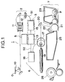
- the image forming apparatus 1 comprises an image reading means 2, an image treating means 3, an image signal generating device 5, an image writing means 6, an image forming means 7 and the like.
- the image reading means 2 is provided with a lighting device 10 for lighting and scanning an original rested on an original glass support 10 at a predetermined reading position thereof. Light emitted from the lighting device 10 is reflected by the original, and the reflected light is directed to a CCD (photoelectric conversion element) 12 acting as the reading means via an optical system 11 comprising mirrors and lenses.
- the CCD 12 cooperates with the optical system 11 to convert an original image into an input image signal S1 (electric signal) of eight-bit with the resolving power of 400 dpi.
- the image treating means 3 has a look-up table (LUT) 13 which is an image signal conversion table through which the input image signal S1 from the CCD 12 is treated to be outputted as an output image signal S2.
- An auxiliary table 15 is connected to the LUT 13 to correct an image data of the LUT 13.
- the LUT 13 and the auxiliary table 15 will be fully described later.
- the image signal generating device 5 is connected to the image treating means 3 so that it can generate any reference image signal for the LUT 13 of the image treating means 3 at any pattern and also generate a predetermined check pattern.
- a predetermined check pattern For example, from this check pattern, an image pattern as shown in Fig. 7 is formed through a predetermined image forming process including the image forming means 7 which will be described later.
- the image pattern is so formed that the density thereof from a while portion (00h) to a black portion (FFh) is gradually increased at seventeen steps per 10h (incidentally, the values 00h, FFh, 10h and the like are hexadecimal numbers, and the explanation of the intermediate steps will not be omitted).
- the image writing-in means 6 has a laser driver circuit 16 for driving a semi-conductor laser 17 on the basis of the output image signal S2 from the LUT 13.
- a laser beam emitted from the semi-conductor laser 17 is deflected by a rotating polygonal reflection mirror 19 and then is sent to a photosensitive drum (image bearing member) 21 via a mirror 20.
- the image forming means 7 comprises a charger 22, a developing device 23 and a cleaner 25 which are arranged around the photosensitive drum 21 and is so designed that the photosensitive drum 21 is uniformly charged by the charger 22, an electrostatic latent image is formed on the photosensitive drum by illuminating the laser light thereon to perform the exposure, and the latent image is developed by the developing device 23 with developer (toner) as a toner image.
- the toner image is transferred onto a recording sheet P supplied from a sheet supply and feed device (not shown) to the photosensitive drum 21, and then is fixed to the recording sheet by a fixing device 26. Thereafter, the recording sheet is ejected out of the image forming apparatus 1 as a finished output image (copy).
- a look-up table 13 having a property curve shown in Fig. 3 is formed in the manner described in connection with Fig. 2 as a conventional case.
- the look-up table (LUT) 13 serves to convert the image signal, i.e., a value of the input image signal S1 from the image reading means 2 into a value of the output image signal S2 which is to be outputted to the image writing-in means 6.
- the image data are outputted by the image signal generating device 5 connected to the image treating means 3 of the image forming system at seventeen steps per 10h (hexadecimal number) from 00h to FFh.
- the image data are sent to the image writing means 6 and the image forming means 7 via the LUT 13 and are outputted on the recording sheet P as the image pattern through the predetermined developing process.
- a stripe-pattern the density D1 of which is gradually increased from the white portion to the black portion is outputted as the image pattern.
- the recording sheet on which the image pattern was formed is rested on the reading position (original glass support), and the density of the image pattern is read by the image reading means 2.
- the output property of the image forming means 7 is not changed from the property when the LUT 13 is formed, the input image signal S1 inputted to the image treating means 3 from the image reading means 2 is to be the same as the output image signal S2 outputted from the image treating means 3 to the image forming means 7, as shown by a straight line (d) in Fig. 4.
- the auxiliary table 15 is formed in the same manner as the formation of the normal LUT 13 to correct the difference, thereby correcting the data in the LUT 13 to correspond to the property of the image forming means 7 at this point. Accordingly, by converting the input image signal S1 into the output image signal S2 through the auxiliary table 15 and the LUT 13, it is possible to always provide the proper image density D1 of the whole image, regardless of the deterioration of the property of the image forming means 7.
- the LUT 13 which is firstly set should not correct the relation between the output image signal S2 and the output image density D1 linearly, but may correct non-linearly.
- Fig. 5 shows another embodiment of the present invention.
- the formation of the look-up table is effected by the image forming apparatus itself so that the LUT 13 and the auxiliary table 15 as in the previous embodiment are unified in one lot. Since the construction and function of the image forming apparatus according to this embodiment are similar to those of the previous embodiment, only the difference will be described.
- the auxiliary table 15 as in the previous embodiment is not provided, and thus, the input image signal S1 is directly inputted to a look-up table (LUT) 13' without passing through any auxiliary table.
- the image signal generating device 5 is not connected to the LUT 13' but to the laser driver circuit 16 of the image writing means 6 so that the image signal from the image signal generating device 5 is directly inputted to the laser driver circuit 16 without passing through the LUT 13'.
- the check pattern the image density of which is gradually and steppingly varied is outputted.
- the check pattern does not pass through the LUT 13'.
- the output property of the image forming means 7 at this point can be judged.
- the LUT 13' is formed in the same manner as the formation of the normal LUT. In the formation of the LUT 13', since the image data are seventeen, the data between these image data are sought by the linear interpolation (Fig. 6).
- the image pattern was read.
- the recording sheet P is fed in a direction B (Fig. 7) at the image forming means, although the dispersion in the density can be averaged regarding a direction A (widthwise direction of the recording sheet P) perpendicular to the direction B, the unevenness of the density in the direction B is apt to affect an influence. That is, since the each step of density (for example, 70h) is formed substantially along a straight line, the difference in density in the longitudinal direction can be detected, but it is difficult to detect the difference in density in the widthwise direction. Namely, the output property can merely be detected linearly.
- the image density of which is varied in both longitudinal and widthwise directions as shown in Fig. 8 it is possible to perform the correction more properly as a whole.
- the image pattern as shown in Fig. 8 since the difference in the output image density D1 regarding the same image data can be detected, it is possible to detect the abnormity in the image forming apparatus. More particularly, if the dispersion or difference in the density regarding the same pattern is greater than 10h, it is assumed that the abnormity in the image forming apparatus occurs; by such diagnostic routine, it is possible to check the image forming apparatus.
- Fig. 9 shows a further embodiment of the present invention.
- the reference numeral 10 denotes a lighting device 10 for lighting an original rested on an original glass support 0; 11 denotes an optical system for projecting an original image; 12 denotes a CCD (reading means) for cooperating with the optical system to convert the original image into an electric signal of eight-bit with the resolving power of 400 dpi; 84 denotes an image treating device for treating an image signal; and 85 denotes a laser driver circuit for driving a semi-conductor laser unit (laser light source) 17 in response to the image signal.
- a lighting device 10 for lighting an original rested on an original glass support 0
- 11 denotes an optical system for projecting an original image
- 12 denotes a CCD (reading means) for cooperating with the optical system to convert the original image into an electric signal of eight-bit with the resolving power of 400 dpi
- 84 denotes an image treating device for treating an image signal
- the image treating device 84 is incorporated into a CPU 82, together with a memory 80 storing a light amount table corresponding to the image density, and a calculating means 81.
- the laser driver circuit 85 incorporates therein an auto power controller (referred to as "APC” hereinafter) 83 acting as a control means for monitoring the light amount of the laser and for correcting the light amount of the semi-conductor laser unit 17 on the basis of the comparison result from the calculating means 81.
- APC auto power controller
- a laser beam emitted from the semi-conductor laser unit 17 is deflected by a rotating polygonal reflection mirror 19 and then is sent to a photosensitive drum 21 via a mirror 20.
- the reference numeral 7 denotes an electrophotographic image forming portion; 23 denotes a developing device; 26 denotes a fixing device; and 5 denotes an image signal generating device (generating means) for generating any image signal (reference signal) at any pattern.
- Figs. 10A to 10D are views for explaining the semi-conductor laser unit 17.
- Fig. 10A shows an appearance of the laser unit.
- the semi-conductor laser unit 17 comprises a semi-conductor laser element 61 and a collimator lens 62 (Fig. 10B) which are housed in a lens-barrel 86 (Fig. 10A).
- the semi-conductor laser element 61 includes a semi-conductor laser chip 611 mounted on a stay 612 made of copper.
- the laser beams are emitted forwardly and rearwardly as shown in Fig. 10D.
- the forward laser beam comes out from a case 614 through a window 613, and the rearward laser beam is illuminated on a laser light intensity monitoring pin photodiode (referred to as "PD" hereinafter) 615.
- PD laser light intensity monitoring pin photodiode
- the wave length of the semi-conductor laser is 780 nm.
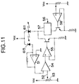
- Fig. 11 is a circuit diagram for explaining the semi-conductor laser driver circuit 85.
- the APC 83 operates as follows.
- the above-mentioned semi-conductor laser chip 611 and DP 615 are depicted in the circuit.
- a current proportional to the laser light amount is inputted to a current/voltage converter 51.
- the reference numeral 52 denotes a target value for the light amount of the emitted laser, which is set by a volume 53.
- the actual light amount is compared with the target value by a comparator 54, and an output from the comparator 54 controls a constant current circuit 55.
- the constant current circuit 55 acts as a bias current source for the semi-conductor laser.
- the reference numeral 56 denotes a data signal for turning the laser ON/OFF; and 57 denotes a high speed switching element of GaAs system for controlling the current in response to the data signal (voltage signal).
- a constant current circuit 58 provides a drive current for turning the semi-conductor laser ON/OFF.
- any check reference signal for example, check reference signal regarding a halftone image
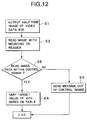
- the semi-conductor laser unit 17 emits the laser light to form an image on the photosensitive drum 21 (step S1).
- the light amount of the laser is monitored by the APC 83.
- the formed image is transferred onto a recording sheet P.
- This recording sheet is then rested on the original glass support 0, and the image on the recording sheet is read by the lighting device 10 and the optical system 11 photoelectrically (step S2).
- the read image is converted into the image signal by the conversion means, and the density data of the image is compared with the light amount table in the memory 80 (Fig. 13A) by the calculating means 81 (step S3). If the read image data is within a control range, the APC 83 corrects the laser light amount (upon the emission of the check signal) on the basis of the comparison result from the calculating means 81.
- the measured image data is of eight-bit from 0 to 255 (0 is all white, 255 is all black, and the other are grey steps).
- the data has normally a HEX (hexadecimal) form.
- the read value should be 80h (underlined) (it has been so set initially).
- the target value of the APC 83 is initially set at 5. In this condition, the laser 17 can be powered up by 4 steps at the maximum. In other words, the reserve power of the APC target value is +4.
- This graph of Fig. 13A indicates that, if the density of the image is decreased due to the deterioration of the image forming apparatus or the like, the control can be effected by the read value of 40h.
- the upper limit of the control depends upon the upper limit of the laser power
- the upper limit of the control can be determined in dependence upon the APC target value when the image is read, as follows: 80h - (9 - present target value)
- x 10h upper limit of control range Since, if the APC target value excdees 9, it is feared that the semi-conductor laser unit 17 is broken, when the control to be performed is out of this control range, a message for checking the image forming apparatus is emitted (step S5 in Fig. 12).
- Fig. 13B shows the transition or change in the image density in this embodiment.
- the endurance test was effected by using the standard 4% original, and the maximum density D max was measured each 1000 copy sheets.
- the corrections of the image density were effected at 20000, 38000 and 53000 copy sheets, respectively. In any case, the proper image density was restored only by the single feedback.
- the laser light amount is adjusted not merely by changing the current value, but by changing the target value of the APC means, even when the laser element itself is deteriorated for a long time, it is possible to expose the photosensitive drum with proper laser light amount, and thus, to form an image having the stable density gradation.
- the deterioration of the image due to endurance revealed itself as the reduction in the image density for the most part (90% or more).
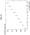
- the APC target values 1 to 4 in the table of Fig. 13A were almost not used. Accordingly, in an embodiment shown in Fig. 14, by setting the initial target value of the APC 83 to 3, it is possible to widen the range of the correction for the reduction in density.
- the APC target value is changed along an upper broken line ( 1 ); whereas, when the measured image data becomes greater, the APC target value is changed along a lower broken line ( 2 ).
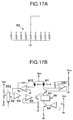
- the APC value was previously set to have a predetermined resistance value, as shown in Fig. 17A (showing the details of the volume 53 of Fig. 11), for the reason that the excessive current is prevented from flowing in the semi-conductor laser unit 17.
- the APC target values were desultory values.
- a limiter circuit 551 is added to the APC circuit. Since the excessive current is prevented from flowing in the semi-conductor laser unit 17 by the limiter circuit 551, the setting values of the APC 83 can be continuously changed by a soft volume 552. A table used in this embodiment is shown in Fig. 16. Since the APC target value can be changed continuously, the control can be effected more smoothly.
- the laser light source is not limited to the semi-conductor laser, but may be a gas laser, a pigment laser or the like.
- the present invention provides an image forming apparatus comprising reading means for converting image light obtained by optically scanning an original into an electric image signal, image signal conversion table for converting the image signal from the reading means in response to the property of the image forming system, image signal generating means for generating a reference image signal, and image forming means for forming an image on a recording sheet in response to the image signal.
- the image is formed on the recording sheet by the image forming means in response to the image signal emitted from the image signal generating means, and image light obtained by optically scanning the recording sheet is converted into an image signal by the reading means, and the image signal conversion table is corrected on the basis of this image signal.
Landscapes
- Engineering & Computer Science (AREA)
- Multimedia (AREA)
- Signal Processing (AREA)
- Physics & Mathematics (AREA)
- Optics & Photonics (AREA)
- Exposure Or Original Feeding In Electrophotography (AREA)
- Control Or Security For Electrophotography (AREA)
- Facsimile Image Signal Circuits (AREA)
- Laser Beam Printer (AREA)
Applications Claiming Priority (4)
| Application Number | Priority Date | Filing Date | Title |
|---|---|---|---|
| JP289207/91 | 1991-10-08 | ||
| JP3289207A JPH05103163A (ja) | 1991-10-08 | 1991-10-08 | 画像形成装置 |
| JP3302350A JPH05114962A (ja) | 1991-10-22 | 1991-10-22 | 画像形成装置 |
| JP302350/91 | 1991-10-22 |
Publications (2)
| Publication Number | Publication Date |
|---|---|
| EP0536733A1 true EP0536733A1 (fr) | 1993-04-14 |
| EP0536733B1 EP0536733B1 (fr) | 1998-05-27 |
Family
ID=26557508
Family Applications (1)
| Application Number | Title | Priority Date | Filing Date |
|---|---|---|---|
| EP92117139A Expired - Lifetime EP0536733B1 (fr) | 1991-10-08 | 1992-10-07 | Méthode de contrÔle d'un appareil de formation d'images |
Country Status (3)
| Country | Link |
|---|---|
| US (1) | US6133934A (fr) |
| EP (1) | EP0536733B1 (fr) |
| DE (1) | DE69225664T2 (fr) |
Cited By (1)
| Publication number | Priority date | Publication date | Assignee | Title |
|---|---|---|---|---|
| EP0596345A1 (fr) * | 1992-11-04 | 1994-05-11 | Eastman Kodak Company | Calibration d'une imprimante à laser |
Families Citing this family (3)
| Publication number | Priority date | Publication date | Assignee | Title |
|---|---|---|---|---|
| CA2126535C (fr) | 1993-12-28 | 2000-12-19 | Ichiro Nomura | Appareil a faisceau electronique et appareil d'imagerie |
| US7162172B2 (en) * | 2004-11-30 | 2007-01-09 | Xerox Corporation | Semi-automatic image quality adjustment for multiple marking engine systems |
| US7379682B2 (en) * | 2005-09-30 | 2008-05-27 | Lexmark International, Inc. | Optimization of operating parameters, including imaging power, in an electrophotographic device |
Citations (4)
| Publication number | Priority date | Publication date | Assignee | Title |
|---|---|---|---|---|
| EP0264886A2 (fr) * | 1986-10-20 | 1988-04-27 | Fuji Photo Film Co., Ltd. | Procédé et appareil d'analyse à faisceau laser |
| EP0269033A2 (fr) * | 1986-11-25 | 1988-06-01 | E.I. Du Pont De Nemours And Company | Système de réglage d'exposition pour films électrographiques à mouvement continu |
| US4751377A (en) * | 1985-12-27 | 1988-06-14 | Fuji Photo Film Co., Ltd. | Light beam scanning recording apparatus and method of correcting intensity of image to be recorded thereby |
| EP0420573A2 (fr) * | 1989-09-26 | 1991-04-03 | Canon Kabushiki Kaisha | Appareil de contrôle de la quantité de lumière |
Family Cites Families (8)
| Publication number | Priority date | Publication date | Assignee | Title |
|---|---|---|---|---|
| JPH0422600Y2 (fr) * | 1985-07-02 | 1992-05-25 | ||
| US4710785A (en) * | 1986-12-12 | 1987-12-01 | Eastman Kodak Company | Process control for electrostatographic machine |
| US4779106A (en) * | 1986-12-12 | 1988-10-18 | Eastman Kodak Company | Process control for electrostatographic machine |
| US5202773A (en) * | 1989-12-22 | 1993-04-13 | Fuji Xerox Co., Ltd. | Multiple value image input device with chromatic gradation correction |
| US5214518A (en) * | 1989-12-22 | 1993-05-25 | Fuji Xerox Co., Ltd. | Multiple value image input equipment |
| JP3143484B2 (ja) * | 1991-02-22 | 2001-03-07 | キヤノン株式会社 | 画像処理装置 |
| US5504517A (en) * | 1991-04-04 | 1996-04-02 | Canon Kabushiki Kaisha | Laser scanner control circuit which is used in image forming apparatus and driver IC for use in such a circuit |
| US5155529A (en) * | 1991-04-22 | 1992-10-13 | Rushing Allen J | Detection of transfer and fusing problems in electrostatographic machines |
-
1992
- 1992-10-07 EP EP92117139A patent/EP0536733B1/fr not_active Expired - Lifetime
- 1992-10-07 DE DE69225664T patent/DE69225664T2/de not_active Expired - Fee Related
-
1995
- 1995-09-13 US US08/527,383 patent/US6133934A/en not_active Expired - Fee Related
Patent Citations (4)
| Publication number | Priority date | Publication date | Assignee | Title |
|---|---|---|---|---|
| US4751377A (en) * | 1985-12-27 | 1988-06-14 | Fuji Photo Film Co., Ltd. | Light beam scanning recording apparatus and method of correcting intensity of image to be recorded thereby |
| EP0264886A2 (fr) * | 1986-10-20 | 1988-04-27 | Fuji Photo Film Co., Ltd. | Procédé et appareil d'analyse à faisceau laser |
| EP0269033A2 (fr) * | 1986-11-25 | 1988-06-01 | E.I. Du Pont De Nemours And Company | Système de réglage d'exposition pour films électrographiques à mouvement continu |
| EP0420573A2 (fr) * | 1989-09-26 | 1991-04-03 | Canon Kabushiki Kaisha | Appareil de contrôle de la quantité de lumière |
Non-Patent Citations (1)
| Title |
|---|
| PATENT ABSTRACTS OF JAPAN vol. 7, no. 214 (E-199)(1359) 21 September 1983 & JP-A-58 106 953 ( RICOH KK ) 25 June 1983 * |
Cited By (1)
| Publication number | Priority date | Publication date | Assignee | Title |
|---|---|---|---|---|
| EP0596345A1 (fr) * | 1992-11-04 | 1994-05-11 | Eastman Kodak Company | Calibration d'une imprimante à laser |
Also Published As
| Publication number | Publication date |
|---|---|
| EP0536733B1 (fr) | 1998-05-27 |
| DE69225664D1 (de) | 1998-07-02 |
| US6133934A (en) | 2000-10-17 |
| DE69225664T2 (de) | 1998-12-03 |
Similar Documents
| Publication | Publication Date | Title |
|---|---|---|
| US5912694A (en) | Laser diode driving circuit, semiconductor integrated circuit for driving laser diode, and image recording apparatus | |
| US6370175B1 (en) | Laser beam luminous energy correction method, laser driving apparatus, laser beam scanner and image recording device | |
| US5966395A (en) | Semiconductor laser drive device and image recording device | |
| JPH0422600Y2 (fr) | ||
| US6324197B1 (en) | Power controller for semiconductor laser device | |
| CN107870540B (zh) | 图像形成装置 | |
| US5726437A (en) | Light intensity control device | |
| US5491506A (en) | Light quantity setting value determination with improved reliability | |
| JP3245205B2 (ja) | 画像形成装置 | |
| US6259466B1 (en) | Light source drive apparatus and image formation apparatus | |
| KR100498666B1 (ko) | 발광 제어 장치 및 화상 형성 장치 | |
| US5473153A (en) | Light intensity control circuit for an optical scanning unit | |
| JPH0969662A (ja) | 光走査装置の光強度変調回路 | |
| US6133934A (en) | Image forming apparatus having an image conversion table for correcting a property of the apparatus | |
| US20170153588A1 (en) | Image forming apparatus using test images to adjust position of latent image | |
| US5305337A (en) | Laser controller | |
| US20080084469A1 (en) | Image forming apparatus and method of controlling the same | |
| US5959650A (en) | Apparatus for forming an image with use of electrophotographic process | |
| US5859659A (en) | Laser beam scanning device and method including light intensity adjustment | |
| US5719613A (en) | Apparatus for forming an image with use of electrophotographic process | |
| JPH0698104A (ja) | Ld駆動回路およびシェーディング補正方法 | |
| JP2002225344A (ja) | 画像形成方法および画像形成装置 | |
| JP3135281B2 (ja) | 画像形成装置 | |
| US5754922A (en) | Automatic exposure adjusting method and apparatus | |
| US5950039A (en) | Image forming apparatus having circuits for adjusting light beam intensity and diameter |
Legal Events
| Date | Code | Title | Description |
|---|---|---|---|
| PUAI | Public reference made under article 153(3) epc to a published international application that has entered the european phase |
Free format text: ORIGINAL CODE: 0009012 |
|
| AK | Designated contracting states |
Kind code of ref document: A1 Designated state(s): DE FR GB IT |
|
| 17P | Request for examination filed |
Effective date: 19930831 |
|
| 17Q | First examination report despatched |
Effective date: 19951031 |
|
| GRAG | Despatch of communication of intention to grant |
Free format text: ORIGINAL CODE: EPIDOS AGRA |
|
| GRAG | Despatch of communication of intention to grant |
Free format text: ORIGINAL CODE: EPIDOS AGRA |
|
| GRAH | Despatch of communication of intention to grant a patent |
Free format text: ORIGINAL CODE: EPIDOS IGRA |
|
| GRAH | Despatch of communication of intention to grant a patent |
Free format text: ORIGINAL CODE: EPIDOS IGRA |
|
| GRAA | (expected) grant |
Free format text: ORIGINAL CODE: 0009210 |
|
| AK | Designated contracting states |
Kind code of ref document: B1 Designated state(s): DE FR GB IT |
|
| REF | Corresponds to: |
Ref document number: 69225664 Country of ref document: DE Date of ref document: 19980702 |
|
| ITF | It: translation for a ep patent filed | ||
| ET | Fr: translation filed | ||
| PLBE | No opposition filed within time limit |
Free format text: ORIGINAL CODE: 0009261 |
|
| 26N | No opposition filed | ||
| REG | Reference to a national code |
Ref country code: GB Ref legal event code: IF02 |
|
| PGFP | Annual fee paid to national office [announced via postgrant information from national office to epo] |
Ref country code: DE Payment date: 20071004 Year of fee payment: 16 |
|
| PGFP | Annual fee paid to national office [announced via postgrant information from national office to epo] |
Ref country code: IT Payment date: 20071026 Year of fee payment: 16 |
|
| PGFP | Annual fee paid to national office [announced via postgrant information from national office to epo] |
Ref country code: FR Payment date: 20071009 Year of fee payment: 16 Ref country code: GB Payment date: 20071003 Year of fee payment: 16 |
|
| GBPC | Gb: european patent ceased through non-payment of renewal fee |
Effective date: 20081007 |
|
| REG | Reference to a national code |
Ref country code: FR Ref legal event code: ST Effective date: 20090630 |
|
| PG25 | Lapsed in a contracting state [announced via postgrant information from national office to epo] |
Ref country code: DE Free format text: LAPSE BECAUSE OF NON-PAYMENT OF DUE FEES Effective date: 20090501 Ref country code: IT Free format text: LAPSE BECAUSE OF NON-PAYMENT OF DUE FEES Effective date: 20081007 |
|
| PG25 | Lapsed in a contracting state [announced via postgrant information from national office to epo] |
Ref country code: FR Free format text: LAPSE BECAUSE OF NON-PAYMENT OF DUE FEES Effective date: 20081031 |
|
| PG25 | Lapsed in a contracting state [announced via postgrant information from national office to epo] |
Ref country code: GB Free format text: LAPSE BECAUSE OF NON-PAYMENT OF DUE FEES Effective date: 20081007 |