EP0536733B1 - Méthode de contrÔle d'un appareil de formation d'images - Google Patents
Méthode de contrÔle d'un appareil de formation d'images Download PDFInfo
- Publication number
- EP0536733B1 EP0536733B1 EP92117139A EP92117139A EP0536733B1 EP 0536733 B1 EP0536733 B1 EP 0536733B1 EP 92117139 A EP92117139 A EP 92117139A EP 92117139 A EP92117139 A EP 92117139A EP 0536733 B1 EP0536733 B1 EP 0536733B1
- Authority
- EP
- European Patent Office
- Prior art keywords
- image
- light amount
- image signal
- laser beam
- generating means
- Prior art date
- Legal status (The legal status is an assumption and is not a legal conclusion. Google has not performed a legal analysis and makes no representation as to the accuracy of the status listed.)
- Expired - Lifetime
Links
Images


Classifications
-
- H—ELECTRICITY
- H04—ELECTRIC COMMUNICATION TECHNIQUE
- H04N—PICTORIAL COMMUNICATION, e.g. TELEVISION
- H04N1/00—Scanning, transmission or reproduction of documents or the like, e.g. facsimile transmission; Details thereof
- H04N1/40—Picture signal circuits
- H04N1/407—Control or modification of tonal gradation or of extreme levels, e.g. background level
- H04N1/4076—Control or modification of tonal gradation or of extreme levels, e.g. background level dependent on references outside the picture
- H04N1/4078—Control or modification of tonal gradation or of extreme levels, e.g. background level dependent on references outside the picture using gradational references, e.g. grey-scale test pattern analysis
-
- H—ELECTRICITY
- H04—ELECTRIC COMMUNICATION TECHNIQUE
- H04N—PICTORIAL COMMUNICATION, e.g. TELEVISION
- H04N1/00—Scanning, transmission or reproduction of documents or the like, e.g. facsimile transmission; Details thereof
- H04N1/40—Picture signal circuits
- H04N1/40025—Circuits exciting or modulating particular heads for reproducing continuous tone value scales
- H04N1/40037—Circuits exciting or modulating particular heads for reproducing continuous tone value scales the reproducing element being a laser
Definitions
- the present invention relates to a method for controlling an image forming apparatus of digital type, and more particularly, it relates to a method carried out by an image forming apparatus having a table for coordinating or corresponding an image signal from a reading means to a recording means.
- a laser beam scanning method and apparatus for recording a continuous tone image by scanning a laser beam emitted by a semiconductor laser on a photosensitive material by a beam scanning system, and controlling a drive current for the semiconductor laser based on a light emission level instructing signal corresponding to an image signal, thereby to modulate the intensity of the laser beam.
- the laser beam intensity is detected, and a feedback signal corresponding to the detected intensity is fed back to the light emission level instruction signal.
- the light emission level instruction signal is corrected by a correction table to compensate for nonlinearity of drive current-optical output characteristics of the semiconductor laser and/or nonlinearity of incident light intensity-optical transmittance characteristics of an optical element of the beam scanning system, thereby to make linear the relationship between the intensity of the laser beam based on the corrected light emission level instructing signal and the uncorrected light emission level instruction signal.
- Document EP-A-O 269 033 shows an exposure control system which permits accurate reproduction of optical density levels on a final image. Said system is characterized by a dynamically corrected look-up table. The look-up table is used to calculate each desired exposure intensity level for each image pixel on the basis of data obtained during the exposure and development of an immediately preceding image.
- Document US-A-4,751,377 shows that in a light beam scanning recording apparatus, a light beam is modulated by a modulator according to image signals and is caused to scan a photosensitive recording material, and the recording material is developed.
- the apparatus is provided with a signal converting section which converts image signals to be input into the modulator according to a predetermined conversion table so that desired image densities can be obtained on the recording material.
- a test pattern signal generating section which generates test pattern signals bearing thereon different image densities and inputs them into the modulator as well as an image density measuring system which measures the image densities of the test pattern on the recording material developed after scanning by a light beam modulated according to the test pattern signal are provided.
- a conversion table making section which determines, on the basis of the relation between the test pattern signals and the image densities of the test pattern measured by the image density measuring system and desired image signal-image density characteristics, the image signals corresponding to the image densities obtained by the respective test pattern signals referring to the desired image signal-image density characteristics, thereby obtaining the relation between the image signals and the test pattern signals, and makes the conversion table on the basis of the relation between the image signals and the test pattern signal.
- a conversion table for coordinating an image signal from a reading means for reading an original to a recording means.
- a conversion table cannot perform the proper conversion, thus arising a problem that an outputted image differs froma desired one.
- an image signal conversion table (referred to as "LUT” or “look up table” hereinafter) is used for correcting the output property of the apparatus and for emphasizing a specific density area.
- LUT image signal conversion table
- the look-up table is incorporated into the image treating means and serves to convert an input image signal inputted from the image reading means to the image treating means into an output image signal which is in turn inputted to the image writing means.
- the look-up table is formed in consideration of the output property of the printer, if the output property of the printer is varied, for example, by the "deterioration and/or contamination" of an image forming means of the printer, the look-up table cannot perform the proper correction. Further, if the value to be corrected is too great (for example, when the actual output property greatly deviated from the ideal output property (straight line) should be corrected to a value on the straight line), the look-up table has the tendency to emphasize the minor change in the output property greatly, and thus, the look-up table is not suitable in the practical use.
- an image forming apparatus having a light amount table for coordinating an image density signal from a reading means to a laser amount of a recording means, when parts of the apparatus are deteriorated or the environmental conditions are changed, the light amount table cannot operate correctly, thus arising a problem that a proper image cannot be reproduced.
- An object of the present invention is to provide a method for controlling an image forming apparatus having a light amount table, which can reproduce the proper image even if the property of the apparatus is varied.
- Fig. 1 shows an apparatus for carrying out a method according to an embodiment of the present invention.
- the reference numeral 10 denotes a lighting device 10 for lighting an original rested on an original glass support 0; 11 denotes an optical system for projecting an original image; 12 denotes a CCD (reading means) for cooperating with the optical system to convert the original image into an electric signal of eight-bit with the resolving power of 400 dpi; 84 denotes an image treating device for treating an image signal; and 85 denotes a laser driver circuit for driving a semi-conductor laser unit (laser light source) 17 in response to the image signal.
- a lighting device 10 for lighting an original rested on an original glass support 0
- 11 denotes an optical system for projecting an original image
- 12 denotes a CCD (reading means) for cooperating with the optical system to convert the original image into an electric signal of eight-bit with the resolving power of 400 dpi
- 84 denotes an image treating
- the image treating device 84 is incorporated into a CPU 82, together with a memory 80 storing a light amount table corresponding to the image density, and a calculating means 81.
- the laser driver circuit 85 incorporates therein an auto power controller (referred to as "APC” hereinafter) 83 acting as a control means for monitoring the light amount of the laser and for correcting the light amount of the semi-conductor laser unit 17 on the basis of the comparison result from the calculating means 81.
- APC auto power controller
- a laser beam emitted from the semi-conductor laser unit 17 is deflected by a rotating polygonal reflection mirror 19 and then is sent to a photosensitive drum 21 via a mirror 20.
- the reference numeral 7 denotes an electrophotographic image forming portion; 23 denotes a developing device; 26 denotes a fixing device; and 5 denotes an image signal generating device (generating means) for generating any image signal (reference signal) at any pattern.
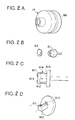
- Figs. 2A to 2D are views for explaining the semi-conductor laser unit 17.
- Fig. 2A shows an appearance of the laser unit.
- the semi-conductor laser unit 17 comprises a semi-conductor laser element 61 and a collimator lens 62 (Fig. 2B) which are housed in a lens-barrel 86 (Fig. 2A).
- the semi-conductor laser element 61 includes a semi-conductor laser chip 611 mounted on a stay 612 made of copper.
- the laser beams are emitted forwardly and rearwardly as shown in Fig. 2D.
- the forward laser beam comes out from a case 614 through a window 613, and the rearward laser beam is illuminated on a laser light intensity monitoring pin photodiode (referred to as "PD" hereinafter) 615.
- PD laser light intensity monitoring pin photodiode
- the wave length of the semi-conductor laser is 780 nm.
- Fig. 3 is a circuit diagram for explaining the semi-conductor laser driver circuit 85.
- the APC 83 operates as follows.
- the above-mentioned semi-conductor laser chip 611 and DP 615 are depicted in the circuit.
- a current proportional to the laser light amount is inputted to a current/voltage converter 51.
- the reference numeral 52 denotes a target value for the light amount of the emitted laser, which is set by a volume 53.
- the actual light amount is compared with the target value by a comparator 54, and an output from the comparator 54 controls a constant current circuit 55.
- the constant current circuit 55 acts as a bias current source for the semi-conductor laser.
- the reference numeral 56 denotes a data signal for turning the laser ON/OFF; and 57 denotes a high speed switching element of GaAs system for controlling the current in response to the data signal (voltage signal).
- a constant current circuit 58 provides a drive current for turning the semi-conductor laser ON/OFF.
- step S1 the operation of the image forming apparatus of Fig, 1 will be explained with reference to a flow chart shown in Fig. 4.
- the semi-conductor laser unit 17 emits the laser light to form an image on the photosensitive drum 21 (step S1).
- the light amount of the laser is monitored by the APC 83.
- the formed image is transferred onto a recording sheet P.
- This recording sheet is then rested on the original glass support 0, and the image on the recording sheet is read by the lighting device 10 and the optical system 11 photoelectrically (step S2).
- the read image is converted into the image signal by the conversion means, and the density data of the image is compared with the light amount table in the memory 80 (Fig. 5A) by the calculating means 81 (step S3). If the read image data is within a control range, the APC 83 corrects the laser light amount (upon the emission of the check signal) on the basis of the comparison result from the calculating means 81.
- the measured image data is of eight-bit from 0 to 255 (0 is all white, 255 is all black, and the other are grey steps).
- the data has normally a HEX (hexadecimal) form.
- the read value should be 80h (underlined) (it has been so set initially).
- the target value of the APC 83 is initially set at 5. In this condition, the laser 17 can be powered up by 4 steps at the maximum. In other words, the reserve power of the APC target value is +4.
- This graph of Fig. 5A indicates that, if the density of the image is decreased due to the deterioration of the image forming apparatus or the like, the control can be effected by the read value of 40h.
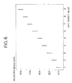
- Fig. 5B shows the transition or change in the image density in this embodiment.
- the endurance test was effected by using the standard 4% original, and the maximum density D max was measured each 1000 copy sheets.
- the corrections of the image density were effected at 20000, 38000 and 53000 copy sheets, respectively. In any case, the proper image density was restored only by the single feedback.
- the laser light amount is adjusted not merely by changing the current value, but by changing the target value of the APC means, even when the laser element itself is deteriorated for a long time, it is possible to expose the photosensitive drum with proper laser light amount, and thus, to form an image having the stable density gradation.
- the deterioration of the image due to endurance revealed itself as the reduction in the image density for the most part (90% or more).
- the APC target values 1 to 4 in the table of Fig. 5A were almost not used. Accordingly, in an embodiment shown in Fig. 6, by setting the initial target value of the APC 83 to 3, it is possible to widen the range of the correction for the reduction in density.
- the APC target value is changed along an upper broken line (1 ⁇ ); whereas, when the measured image data becomes greater, the APC target value is changed along a lower broken line (2 ⁇ ).
- the APC value was previously set to have a predetermined resistance value, as shown in Fig. 9A (showing the details of the part 53 of Fig. 3), for the reason that the excessive current is prevented from flowing in the semi-conductor laser unit 17.
- the APC target values were desultory values.
- a limiter circuit 551 is added to the APC circuit. Since the excessive current is prevented from flowing in the semi-conductor laser unit 17 by the limiter circuit 551, the setting values of the APC 83 can be continuously changed by a soft volume 552.
- a table used in this apparatus is shown in Fig. 8. Since the APC target value can be changed continuously, the control can be effected more smoothly.
- the laser light source is not limited to the semi-conductor laser, but may be a gas laser, a pigment laser or the like.
Landscapes
- Engineering & Computer Science (AREA)
- Multimedia (AREA)
- Signal Processing (AREA)
- Physics & Mathematics (AREA)
- Optics & Photonics (AREA)
- Exposure Or Original Feeding In Electrophotography (AREA)
- Control Or Security For Electrophotography (AREA)
- Facsimile Image Signal Circuits (AREA)
- Laser Beam Printer (AREA)
Claims (4)
- Procédé de commande d'un appareil de formation d'images, comportant :caractérisé par les étapes dans lesquellesl'émission par un moyen (611) de génération d'un faisceau laser d'un faisceau laser de la même valeur de l'avant à l'arrière de celui-ci en réponse à un signal d'image ;la détection, par un moyen (615) de détection de quantité de lumière, d'une quantité de lumière du faisceau arrière émis depuis ledit moyen (611) de génération de faisceau laser ;la commande par un moyen de commande (55) de la puissance fournie audit moyen (611) de génération de faisceau laser sur la base d'un résultat de comparaison entre la quantité de lumière détectée dudit moyen (615) de détection de quantité de lumière et une valeur réelle (52) de consigne de la quantité de lumière ;la génération, par un moyen (5) de génération de signal d'image, d'un signal d'image de référence ; etla formation, par un moyen (7) de formation d'images, d'une image en émettant le faisceau avant émis depuis ledit moyen (611) de génération de faisceau laser en réponse à un signal d'image ;on forme une image de référence sur une feuille d'enregistrement en émettant le faisceau avant depuis ledit moyen (611) de génération de faisceau laser en réponse audit signal d'image de référence généré par ledit moyen (5) de génération de signal d'image ;on obtient des données de densité de ladite image de référence en convertissant la lumière d'une image obtenue par un balayage optique de ladite image de référence formée sur ladite feuille d'enregistrement, en un signal d'image électrique ;on compare lesdites données de densité à des données d'une table (80) de quantités de lumière ; eton modifie ladite valeur réelle (52) de consigne de quantité de lumière sur la base du résultat de la comparaison entre lesdites données de densité et lesdites données de la table de quantité de lumière.
- Procédé selon la revendication 1, caractérisé par les autres étapes dans lesquelles on détermine si lesdites données de densité obtenues sont comprises dans une plage de commande, et on modifie ladite valeur réelle de consigne de quantité de lumière uniquement si les données de densité obtenues sont comprises dans ladite plage de commande.
- Procédé selon la revendication 2, caractérisé par l'autre étape dans laquelle on calcule la limite supérieure de la plage de commande sur la base desdites données de densité obtenues et de ladite valeur réelle de consigne de quantité de lumière.
- Procédé selon l'une quelconque des revendications précédentes, caractérisé en ce qu'une hystérésis est prévue dans les données de la table de quantités de lumière.
Applications Claiming Priority (4)
| Application Number | Priority Date | Filing Date | Title |
|---|---|---|---|
| JP289207/91 | 1991-10-08 | ||
| JP3289207A JPH05103163A (ja) | 1991-10-08 | 1991-10-08 | 画像形成装置 |
| JP3302350A JPH05114962A (ja) | 1991-10-22 | 1991-10-22 | 画像形成装置 |
| JP302350/91 | 1991-10-22 |
Publications (2)
| Publication Number | Publication Date |
|---|---|
| EP0536733A1 EP0536733A1 (fr) | 1993-04-14 |
| EP0536733B1 true EP0536733B1 (fr) | 1998-05-27 |
Family
ID=26557508
Family Applications (1)
| Application Number | Title | Priority Date | Filing Date |
|---|---|---|---|
| EP92117139A Expired - Lifetime EP0536733B1 (fr) | 1991-10-08 | 1992-10-07 | Méthode de contrÔle d'un appareil de formation d'images |
Country Status (3)
| Country | Link |
|---|---|
| US (1) | US6133934A (fr) |
| EP (1) | EP0536733B1 (fr) |
| DE (1) | DE69225664T2 (fr) |
Families Citing this family (4)
| Publication number | Priority date | Publication date | Assignee | Title |
|---|---|---|---|---|
| US5281979A (en) * | 1992-11-04 | 1994-01-25 | Eastman Kodak Company | Laser printer calibration |
| CA2126535C (fr) | 1993-12-28 | 2000-12-19 | Ichiro Nomura | Appareil a faisceau electronique et appareil d'imagerie |
| US7162172B2 (en) * | 2004-11-30 | 2007-01-09 | Xerox Corporation | Semi-automatic image quality adjustment for multiple marking engine systems |
| US7379682B2 (en) * | 2005-09-30 | 2008-05-27 | Lexmark International, Inc. | Optimization of operating parameters, including imaging power, in an electrophotographic device |
Family Cites Families (12)
| Publication number | Priority date | Publication date | Assignee | Title |
|---|---|---|---|---|
| JPH0422600Y2 (fr) * | 1985-07-02 | 1992-05-25 | ||
| US4751377A (en) * | 1985-12-27 | 1988-06-14 | Fuji Photo Film Co., Ltd. | Light beam scanning recording apparatus and method of correcting intensity of image to be recorded thereby |
| EP0264886B1 (fr) * | 1986-10-20 | 1994-06-08 | Fuji Photo Film Co., Ltd. | Procédé et appareil d'analyse à faisceau laser |
| US4816863A (en) * | 1986-11-25 | 1989-03-28 | E. I. Du Pont De Nemours And Company | Exposure control system for continuous tone electrophotographic film |
| US4710785A (en) * | 1986-12-12 | 1987-12-01 | Eastman Kodak Company | Process control for electrostatographic machine |
| US4779106A (en) * | 1986-12-12 | 1988-10-18 | Eastman Kodak Company | Process control for electrostatographic machine |
| JP2905229B2 (ja) * | 1989-09-26 | 1999-06-14 | キヤノン株式会社 | 光ビーム駆動装置 |
| US5202773A (en) * | 1989-12-22 | 1993-04-13 | Fuji Xerox Co., Ltd. | Multiple value image input device with chromatic gradation correction |
| US5214518A (en) * | 1989-12-22 | 1993-05-25 | Fuji Xerox Co., Ltd. | Multiple value image input equipment |
| JP3143484B2 (ja) * | 1991-02-22 | 2001-03-07 | キヤノン株式会社 | 画像処理装置 |
| US5504517A (en) * | 1991-04-04 | 1996-04-02 | Canon Kabushiki Kaisha | Laser scanner control circuit which is used in image forming apparatus and driver IC for use in such a circuit |
| US5155529A (en) * | 1991-04-22 | 1992-10-13 | Rushing Allen J | Detection of transfer and fusing problems in electrostatographic machines |
-
1992
- 1992-10-07 EP EP92117139A patent/EP0536733B1/fr not_active Expired - Lifetime
- 1992-10-07 DE DE69225664T patent/DE69225664T2/de not_active Expired - Fee Related
-
1995
- 1995-09-13 US US08/527,383 patent/US6133934A/en not_active Expired - Fee Related
Also Published As
| Publication number | Publication date |
|---|---|
| EP0536733A1 (fr) | 1993-04-14 |
| DE69225664D1 (de) | 1998-07-02 |
| US6133934A (en) | 2000-10-17 |
| DE69225664T2 (de) | 1998-12-03 |
Similar Documents
| Publication | Publication Date | Title |
|---|---|---|
| US5912694A (en) | Laser diode driving circuit, semiconductor integrated circuit for driving laser diode, and image recording apparatus | |
| JP3700296B2 (ja) | 半導体レーザ駆動装置および画像記録装置 | |
| US4905023A (en) | Image forming apparatus including digital image signal input means | |
| US5359433A (en) | Image processing apparatus with reduced image deterioration in highlight portions | |
| US5726437A (en) | Light intensity control device | |
| JP3245205B2 (ja) | 画像形成装置 | |
| US5832012A (en) | Laser scanning unit having automatic power control function | |
| US5473153A (en) | Light intensity control circuit for an optical scanning unit | |
| EP0536733B1 (fr) | Méthode de contrÔle d'un appareil de formation d'images | |
| US4984015A (en) | Exposure method and apparatus | |
| US5959650A (en) | Apparatus for forming an image with use of electrophotographic process | |
| JPS63209270A (ja) | 半導体レ−ザのドル−プ補正装置 | |
| US5859659A (en) | Laser beam scanning device and method including light intensity adjustment | |
| US5719613A (en) | Apparatus for forming an image with use of electrophotographic process | |
| US6384856B2 (en) | Image formation apparatus correction system | |
| US20050030435A1 (en) | Image forming method and apparatus | |
| JP2002225344A (ja) | 画像形成方法および画像形成装置 | |
| US5761231A (en) | Method and circuit arrangement for regulating the luminous power of a laser diode | |
| EP0989736B1 (fr) | Procédé et dispositif de contrôle d'un laser avec un seuil de niveau de courant | |
| US6219084B1 (en) | Method and device for controlling a laser having a threshold current level | |
| JP2698099B2 (ja) | 画像形成装置 | |
| JP2003087508A (ja) | 画像形成装置 | |
| JP3197017B2 (ja) | デジタル画像形成法 | |
| JPH05188709A (ja) | 画像形成装置 | |
| JP3728090B2 (ja) | 画像形成装置 |
Legal Events
| Date | Code | Title | Description |
|---|---|---|---|
| PUAI | Public reference made under article 153(3) epc to a published international application that has entered the european phase |
Free format text: ORIGINAL CODE: 0009012 |
|
| AK | Designated contracting states |
Kind code of ref document: A1 Designated state(s): DE FR GB IT |
|
| 17P | Request for examination filed |
Effective date: 19930831 |
|
| 17Q | First examination report despatched |
Effective date: 19951031 |
|
| GRAG | Despatch of communication of intention to grant |
Free format text: ORIGINAL CODE: EPIDOS AGRA |
|
| GRAG | Despatch of communication of intention to grant |
Free format text: ORIGINAL CODE: EPIDOS AGRA |
|
| GRAH | Despatch of communication of intention to grant a patent |
Free format text: ORIGINAL CODE: EPIDOS IGRA |
|
| GRAH | Despatch of communication of intention to grant a patent |
Free format text: ORIGINAL CODE: EPIDOS IGRA |
|
| GRAA | (expected) grant |
Free format text: ORIGINAL CODE: 0009210 |
|
| AK | Designated contracting states |
Kind code of ref document: B1 Designated state(s): DE FR GB IT |
|
| REF | Corresponds to: |
Ref document number: 69225664 Country of ref document: DE Date of ref document: 19980702 |
|
| ITF | It: translation for a ep patent filed | ||
| ET | Fr: translation filed | ||
| PLBE | No opposition filed within time limit |
Free format text: ORIGINAL CODE: 0009261 |
|
| 26N | No opposition filed | ||
| REG | Reference to a national code |
Ref country code: GB Ref legal event code: IF02 |
|
| PGFP | Annual fee paid to national office [announced via postgrant information from national office to epo] |
Ref country code: DE Payment date: 20071004 Year of fee payment: 16 |
|
| PGFP | Annual fee paid to national office [announced via postgrant information from national office to epo] |
Ref country code: IT Payment date: 20071026 Year of fee payment: 16 |
|
| PGFP | Annual fee paid to national office [announced via postgrant information from national office to epo] |
Ref country code: FR Payment date: 20071009 Year of fee payment: 16 Ref country code: GB Payment date: 20071003 Year of fee payment: 16 |
|
| GBPC | Gb: european patent ceased through non-payment of renewal fee |
Effective date: 20081007 |
|
| REG | Reference to a national code |
Ref country code: FR Ref legal event code: ST Effective date: 20090630 |
|
| PG25 | Lapsed in a contracting state [announced via postgrant information from national office to epo] |
Ref country code: DE Free format text: LAPSE BECAUSE OF NON-PAYMENT OF DUE FEES Effective date: 20090501 Ref country code: IT Free format text: LAPSE BECAUSE OF NON-PAYMENT OF DUE FEES Effective date: 20081007 |
|
| PG25 | Lapsed in a contracting state [announced via postgrant information from national office to epo] |
Ref country code: FR Free format text: LAPSE BECAUSE OF NON-PAYMENT OF DUE FEES Effective date: 20081031 |
|
| PG25 | Lapsed in a contracting state [announced via postgrant information from national office to epo] |
Ref country code: GB Free format text: LAPSE BECAUSE OF NON-PAYMENT OF DUE FEES Effective date: 20081007 |