EP0536763A1 - Hologramm und Vorrichtung zum Herstellen einer holographischen Platte - Google Patents
Hologramm und Vorrichtung zum Herstellen einer holographischen Platte Download PDFInfo
- Publication number
- EP0536763A1 EP0536763A1 EP92117231A EP92117231A EP0536763A1 EP 0536763 A1 EP0536763 A1 EP 0536763A1 EP 92117231 A EP92117231 A EP 92117231A EP 92117231 A EP92117231 A EP 92117231A EP 0536763 A1 EP0536763 A1 EP 0536763A1
- Authority
- EP
- European Patent Office
- Prior art keywords
- base plate
- hologram
- hologram element
- reflected
- opposite surfaces
- Prior art date
- Legal status (The legal status is an assumption and is not a legal conclusion. Google has not performed a legal analysis and makes no representation as to the accuracy of the status listed.)
- Granted
Links
Images


Classifications
-
- G—PHYSICS
- G03—PHOTOGRAPHY; CINEMATOGRAPHY; ANALOGOUS TECHNIQUES USING WAVES OTHER THAN OPTICAL WAVES; ELECTROGRAPHY; HOLOGRAPHY
- G03H—HOLOGRAPHIC PROCESSES OR APPARATUS
- G03H1/00—Holographic processes or apparatus using light, infrared or ultraviolet waves for obtaining holograms or for obtaining an image from them; Details peculiar thereto
- G03H1/02—Details of features involved during the holographic process; Replication of holograms without interference recording
- G03H1/0252—Laminate comprising a hologram layer
- G03H1/0256—Laminate comprising a hologram layer having specific functional layer
-
- G—PHYSICS
- G02—OPTICS
- G02B—OPTICAL ELEMENTS, SYSTEMS OR APPARATUS
- G02B27/00—Optical systems or apparatus not provided for by any of the groups G02B1/00 - G02B26/00, G02B30/00
- G02B27/01—Head-up displays
- G02B27/0101—Head-up displays characterised by optical features
- G02B27/0103—Head-up displays characterised by optical features comprising holographic elements
-
- G—PHYSICS
- G02—OPTICS
- G02B—OPTICAL ELEMENTS, SYSTEMS OR APPARATUS
- G02B5/00—Optical elements other than lenses
- G02B5/32—Holograms used as optical elements
-
- B—PERFORMING OPERATIONS; TRANSPORTING
- B60—VEHICLES IN GENERAL
- B60K—ARRANGEMENT OR MOUNTING OF PROPULSION UNITS OR OF TRANSMISSIONS IN VEHICLES; ARRANGEMENT OR MOUNTING OF PLURAL DIVERSE PRIME-MOVERS IN VEHICLES; AUXILIARY DRIVES FOR VEHICLES; INSTRUMENTATION OR DASHBOARDS FOR VEHICLES; ARRANGEMENTS IN CONNECTION WITH COOLING, AIR INTAKE, GAS EXHAUST OR FUEL SUPPLY OF PROPULSION UNITS IN VEHICLES
- B60K2360/00—Indexing scheme associated with groups B60K35/00 or B60K37/00 relating to details of instruments or dashboards
- B60K2360/20—Optical features of instruments
- B60K2360/33—Illumination features
- B60K2360/334—Projection means
-
- G—PHYSICS
- G02—OPTICS
- G02B—OPTICAL ELEMENTS, SYSTEMS OR APPARATUS
- G02B27/00—Optical systems or apparatus not provided for by any of the groups G02B1/00 - G02B26/00, G02B30/00
- G02B27/01—Head-up displays
- G02B27/0101—Head-up displays characterised by optical features
- G02B27/0103—Head-up displays characterised by optical features comprising holographic elements
- G02B2027/0109—Head-up displays characterised by optical features comprising holographic elements comprising details concerning the making of holograms
-
- G—PHYSICS
- G02—OPTICS
- G02B—OPTICAL ELEMENTS, SYSTEMS OR APPARATUS
- G02B27/00—Optical systems or apparatus not provided for by any of the groups G02B1/00 - G02B26/00, G02B30/00
- G02B27/01—Head-up displays
- G02B27/0101—Head-up displays characterised by optical features
- G02B2027/0118—Head-up displays characterised by optical features comprising devices for improving the contrast of the display / brillance control visibility
-
- G—PHYSICS
- G02—OPTICS
- G02B—OPTICAL ELEMENTS, SYSTEMS OR APPARATUS
- G02B27/00—Optical systems or apparatus not provided for by any of the groups G02B1/00 - G02B26/00, G02B30/00
- G02B27/01—Head-up displays
- G02B27/0101—Head-up displays characterised by optical features
- G02B2027/0118—Head-up displays characterised by optical features comprising devices for improving the contrast of the display / brillance control visibility
- G02B2027/012—Head-up displays characterised by optical features comprising devices for improving the contrast of the display / brillance control visibility comprising devices for attenuating parasitic image effects
-
- G—PHYSICS
- G02—OPTICS
- G02B—OPTICAL ELEMENTS, SYSTEMS OR APPARATUS
- G02B27/00—Optical systems or apparatus not provided for by any of the groups G02B1/00 - G02B26/00, G02B30/00
- G02B27/01—Head-up displays
- G02B27/0149—Head-up displays characterised by mechanical features
- G02B2027/0165—Head-up displays characterised by mechanical features associated with a head-down display
-
- G—PHYSICS
- G02—OPTICS
- G02B—OPTICAL ELEMENTS, SYSTEMS OR APPARATUS
- G02B27/00—Optical systems or apparatus not provided for by any of the groups G02B1/00 - G02B26/00, G02B30/00
- G02B27/0018—Optical systems or apparatus not provided for by any of the groups G02B1/00 - G02B26/00, G02B30/00 with means for preventing ghost images
-
- G—PHYSICS
- G03—PHOTOGRAPHY; CINEMATOGRAPHY; ANALOGOUS TECHNIQUES USING WAVES OTHER THAN OPTICAL WAVES; ELECTROGRAPHY; HOLOGRAPHY
- G03H—HOLOGRAPHIC PROCESSES OR APPARATUS
- G03H1/00—Holographic processes or apparatus using light, infrared or ultraviolet waves for obtaining holograms or for obtaining an image from them; Details peculiar thereto
- G03H1/02—Details of features involved during the holographic process; Replication of holograms without interference recording
- G03H1/0252—Laminate comprising a hologram layer
-
- G—PHYSICS
- G03—PHOTOGRAPHY; CINEMATOGRAPHY; ANALOGOUS TECHNIQUES USING WAVES OTHER THAN OPTICAL WAVES; ELECTROGRAPHY; HOLOGRAPHY
- G03H—HOLOGRAPHIC PROCESSES OR APPARATUS
- G03H1/00—Holographic processes or apparatus using light, infrared or ultraviolet waves for obtaining holograms or for obtaining an image from them; Details peculiar thereto
- G03H1/04—Processes or apparatus for producing holograms
- G03H1/0486—Improving or monitoring the quality of the record, e.g. by compensating distortions, aberrations
-
- G—PHYSICS
- G03—PHOTOGRAPHY; CINEMATOGRAPHY; ANALOGOUS TECHNIQUES USING WAVES OTHER THAN OPTICAL WAVES; ELECTROGRAPHY; HOLOGRAPHY
- G03H—HOLOGRAPHIC PROCESSES OR APPARATUS
- G03H1/00—Holographic processes or apparatus using light, infrared or ultraviolet waves for obtaining holograms or for obtaining an image from them; Details peculiar thereto
- G03H1/04—Processes or apparatus for producing holograms
- G03H1/0402—Recording geometries or arrangements
- G03H2001/0415—Recording geometries or arrangements for recording reflection holograms
- G03H2001/0417—Recording geometries or arrangements for recording reflection holograms for recording single beam Lippmann hologram wherein the object is illuminated by reference beam passing through the recording material
-
- G—PHYSICS
- G03—PHOTOGRAPHY; CINEMATOGRAPHY; ANALOGOUS TECHNIQUES USING WAVES OTHER THAN OPTICAL WAVES; ELECTROGRAPHY; HOLOGRAPHY
- G03H—HOLOGRAPHIC PROCESSES OR APPARATUS
- G03H2223/00—Optical components
- G03H2223/18—Prism
-
- G—PHYSICS
- G03—PHOTOGRAPHY; CINEMATOGRAPHY; ANALOGOUS TECHNIQUES USING WAVES OTHER THAN OPTICAL WAVES; ELECTROGRAPHY; HOLOGRAPHY
- G03H—HOLOGRAPHIC PROCESSES OR APPARATUS
- G03H2223/00—Optical components
- G03H2223/25—Index matching material
-
- G—PHYSICS
- G03—PHOTOGRAPHY; CINEMATOGRAPHY; ANALOGOUS TECHNIQUES USING WAVES OTHER THAN OPTICAL WAVES; ELECTROGRAPHY; HOLOGRAPHY
- G03H—HOLOGRAPHIC PROCESSES OR APPARATUS
- G03H2240/00—Hologram nature or properties
- G03H2240/50—Parameters or numerical values associated with holography, e.g. peel strength
- G03H2240/54—Refractive index
-
- G—PHYSICS
- G03—PHOTOGRAPHY; CINEMATOGRAPHY; ANALOGOUS TECHNIQUES USING WAVES OTHER THAN OPTICAL WAVES; ELECTROGRAPHY; HOLOGRAPHY
- G03H—HOLOGRAPHIC PROCESSES OR APPARATUS
- G03H2240/00—Hologram nature or properties
- G03H2240/50—Parameters or numerical values associated with holography, e.g. peel strength
- G03H2240/55—Thickness
-
- G—PHYSICS
- G03—PHOTOGRAPHY; CINEMATOGRAPHY; ANALOGOUS TECHNIQUES USING WAVES OTHER THAN OPTICAL WAVES; ELECTROGRAPHY; HOLOGRAPHY
- G03H—HOLOGRAPHIC PROCESSES OR APPARATUS
- G03H2250/00—Laminate comprising a hologram layer
- G03H2250/32—Antireflective layer
-
- G—PHYSICS
- G03—PHOTOGRAPHY; CINEMATOGRAPHY; ANALOGOUS TECHNIQUES USING WAVES OTHER THAN OPTICAL WAVES; ELECTROGRAPHY; HOLOGRAPHY
- G03H—HOLOGRAPHIC PROCESSES OR APPARATUS
- G03H2250/00—Laminate comprising a hologram layer
- G03H2250/37—Enclosing the photosensitive material
-
- G—PHYSICS
- G03—PHOTOGRAPHY; CINEMATOGRAPHY; ANALOGOUS TECHNIQUES USING WAVES OTHER THAN OPTICAL WAVES; ELECTROGRAPHY; HOLOGRAPHY
- G03H—HOLOGRAPHIC PROCESSES OR APPARATUS
- G03H2250/00—Laminate comprising a hologram layer
- G03H2250/39—Protective layer
-
- G—PHYSICS
- G03—PHOTOGRAPHY; CINEMATOGRAPHY; ANALOGOUS TECHNIQUES USING WAVES OTHER THAN OPTICAL WAVES; ELECTROGRAPHY; HOLOGRAPHY
- G03H—HOLOGRAPHIC PROCESSES OR APPARATUS
- G03H2260/00—Recording materials or recording processes
- G03H2260/10—Dichromated gelatine or equivalents
Definitions
- This invention relates to a hologram. This invention also relates to an apparatus for manufacturing a holographic plate.
- head-up displays Systems commonly used in aircraft to display images of instruments in the field of view of a pilot are termed "head-up displays”. Some of the head-up displays employ holograms to project a virtual image of an instrument into the pilot's field of view as the pilot looks through the forward window of the aircraft.
- holograms used in head-up displays generate an acceptably low level of noise or ghost.
- Japanese published unexamined patent application 62-80687 discloses the fabrication of a hologram in which an antireflection film is formed on a photosensitive film of a hologram-forming base plate (substrate).
- the antireflection film decreases reflection of reference light at the boundary between air and the photosensitive film so that spurious hologram recordings are reduced.
- the reduction of spurious hologram recordings enables a decrease in the level of noise or ghost when an image is reproduced or indicated by using the resultant hologram.
- a first aspect of this invention provides a hologram comprising an optically transparent base plate having first and second opposite surfaces; a hologram element provided on the first surface of the base plate and having a predetermined holographic pattern; an optically transparent member having first and second opposite surfaces, wherein the first surface of the member faces the hologram element; and means for preventing light, which successively passes through the transparent base plate, the hologram element, and the member and is then reflected at a boundary between the second surface of the member and an atmosphere, from travelling back to the hologram element.
- a second aspect of this invention provides a hologram comprising an optically transparent base plate having first and second opposite surfaces; a hologram element provided on the first surface of the base plate and having a predetermined holographic pattern; a first reflection control layer being optically transparent and being provided at a side of the second surface of the base plate for preventing light, which is applied toward the second surface of the base plate and is reflected at a boundary between the second surface of the base plate and an atmosphere, from travelling in a direction equal to a direction of travel of reconstructed light generated via the hologram element; an optically transparent member having first and second opposite surfaces, wherein the first surface of the member faces the hologram element; and a second reflection control layer provided on the second surface of the member for preventing light, which successively passes through the transparent base plate, the hologram element, and the member and is then reflected at a boundary between the second surface of the member and an atmosphere, from travelling back to the hologram element.
- a third aspect of this invention provides a hologram comprising an optically transparent base plate having first and second opposite surfaces; a hologram element provided on the first surface of the base plate and having a predetermined holographic pattern; a first optically transparent member having first and second opposite surfaces, wherein the first surface of the first member faces the hologram element; first means for preventing light, which successively passes through the transparent base plate, the hologram element, and the first member and is then reflected at a boundary between the second surface of the first member and an atmosphere, from travelling back to the hologram element; a second optically transparent member having first and second opposite surfaces, wherein the first surface of the second member faces the second surface of the base plate; and second means for preventing light, which is applied toward the second surface of the second member and is reflected at a boundary between the second surface of the second member and an atmosphere, from travelling in a direction equal to a direction of travel of reconstructed light generated via the hologram element.
- a fourth aspect of this invention provides an apparatus for manufacturing a holographic plate which comprises an optically transparent base plate having first and second opposite surfaces; a hologram-forming photosensitive layer provided on the first surface of the base plate; an optical element for copy which has first and second opposite surfaces, wherein the first surface of the element faces the photosensitive layer; a reflecting film formed on the second surface of the element; and means for preventing light, which successively passes through the transparent base plate, the photosensitive layer, and the element and is then reflected by the reflecting film and successively passes through the element, the photosensitive layer, and the transparent base plate, from being reflected at the second surface of the base plate.
- the member and the first and second members serve to cover the base plate, they may also be referred to as cover members or cover plates.
- the cover members and the base plate may be made of glass such as soda glass or various plastics. It is preferable that a surface of the first member which faces an atmosphere has an antireflection film. It is preferable that a surface of the second member which faces an atmosphere has an anti-scattering film.
- the anti-scattering film has such a light absorbing function as to prevent light, which successively passes through the transparent base plate, the hologram element, and the first member and is then reflected at a boundary between the second surface of the first member and an atmosphere, from travelling back to the hologram element.
- the antireflection film serves to prevent light, which is applied toward the hologram element via the second surface of the second member, from being reflected at a boundary between the second surface of the second member and an atmosphere.
- the anti-scattering film may use a tape or a mixture of black or other pigment and epoxy, melanin, acrylic, or other synthetic resin binder.
- the anti-scattering film may also be made of a black paint.
- the antireflection film may be mode of MgF2, TiO2, ZrO2, or SiO2.
- the antireflection film may be composed of a single layer of MgF2, TiO2, ZrO2, or SiO2.
- the antireflection film may have a laminated structure of layers of these substances.
- the refractive indexes of the member, the first and second members, and the base plate are substantially equal to the refractive index of the dichromated gelatin layer.
- the refractive indexes of the member, the first and second members, and the base plate are preferably in the range of 1.5 to 1.6.
- the member and the base plate with the hologram element may be bonded together by sealing material provided therebetween.
- the first member, the base plate with the hologram element, and the second member may be bonded together by sealing material provided therebetween.
- the sealing material is made of organic resin of an ultraviolet-ray hardening type or organic resin of a thermosetting type.
- the sealing material may be designed so as to protect the hologram element from moisture of an atmosphere.
- a sealing width "W” is defined as a width of a region filled with only the sealing material by which the hologram element is separated from an atmosphere.
- the sealing width "W” is chosen in consideration of moisture absorption characteristics of the sealing material and conditions of practical use of the hologram.
- the sealing width "W” is shown in Figs. 1 and 2.
- the hologram element is made by exposing photopolymer or photosensitive material, such as dichromated gelatin, agar, or albumen, to light.
- the hologram element is most preferably made of dichromated gelatin.
- the hologram element may be of an embossed structure.
- a medium (corresponding to a holographic pattern) recorded on the photosensitive material, that is, the hologram element, is a lens in embodiments of this invention. Letters, numerals, or pictures may be recorded on the hologram element as a recorded medium.
- Laser light is used in the exposure process on the photosensitive material.
- interference fringes of the laser light which correspond to the holographic pattern are recorded on the photosensitive material.
- the pitch of the interference fringes on the photosensitive material can be varied by changing the incident angle of the laser light with respect to the photosensitive material. It is understood from the characteristics of Bragg reflection that the wavelength of light reconstructed by the hologram element depends on the pitch of the holographic pattern on the hologram element.
- holographic patterns having different pitches can be recorded on the photosensitive material. This technique enables the addition of a filtering function to the hologram element.
- a hologram element having holographic patters of different pitches when a white light beam is applied to the hologram element, light beams of different colors can be reconstructed.
- optical transparent means both “fully transparent” and “semitransparent”. In a special case, “optically transparent” means “opaque”.
- This invention can suppress the surface reflection and the scattering of transmission light passing through the hologram element which would cause noise or ghost light.
- a light beam is incident to one surface of the base plate.
- the incident light beam successively passes through the base plate, the photosensitive layer, and the element for copy, and is then reflected by the reflecting film on one surface of the element for copy.
- the resultant reflected light beam successively passes through the element for copy, the photosensitive layer, and the base plate. Since a re-reflection preventing device is provided on the surface of the base plate, the reflected light passes through and exits from the base plate without being reflected at a boundary between the base plate and the re-reflection preventing device.
- Fig. 1 is a sectional view of a hologram according to an embodiment of this invention.
- Fig. 2 is a plan view of the hologram of Fig. 1.
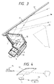
- Fig. 3 is a sectional view of an automotive head-up display using the hologram of Figs. 1 and 2.
- Fig. 4 is a perspective diagram of the automotive head-up display of Fig. 3.
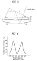
- Fig. 5 is a sectional view of an optical arrangement used in the fabrication of the hologram of Figs. 1 and 2.
- Fig. 6 is a diagram showing the relation between the diffraction efficiency and the reconstructed light wavelength in holograms in embodiments of this invention.
- Fig. 7 is a diagram showing the noise ratios of examples of holograms in embodiments of this invention.
- Fig. 8 is a sectional view of a first modified hologram according to an embodiment of this invention.
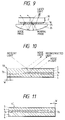
- Fig. 9 is a sectional view of an optical arrangement used in the fabrication of a hologram.
- Fig. 10 is a sectional view of a second modified hologram according to an embodiment of this invention.
- Fig. 11 is a sectional view of a third modified hologram according to an embodiment of this invention.
- a hologram 1 includes a transparent base plate (substrate) 2 made of glass and having, for example, a rectangular shape.
- the base plate 2 has a predetermined uniform thickness.
- the base plate 2 has opposite larger surfaces, that is, upper and lower surfaces in Fig. 1.
- a given area of the lower surface of the base plate 2 except edges thereof is provided or coated with a film of a hologram element 1a which has a predetermined uniform thickness and which has a rectangular shape similar to but smaller than the shape of the base plate 2.
- the hologram element 1a holds a predetermined pattern or a predetermined recorded medium.
- the predetermined pattern (the recorded medium) provided by interference fringes are recorded on the photosensitive material.
- the recorded medium corresponds to a concave lens serving as a magnifying lens.
- Interference fringes having a pitch of 290 nm and interference fringes having a pitch of 320 nm are recorded on the hologram element 1a. These recordings are executed by changing a direction or angle of a laser light beam being incident to the photosensitive material and forming the interference fringes.
- the interference fringes are of two different shape types having predetermined curvatures to simultaneously record information of the concave lens and information of color.
- a transparent cover plate 3 made of glass extends above the base plate 2.
- the cover plate 3 has a rectangular shape equal to the shape of the base plate 2 and is aligned with the base plate 2.
- the cover plate 3 has a predetermined uniform thickness.
- the cover plate 3 has opposite larger surfaces, that is, upper and lower surfaces in Fig. 1.
- the entire area of the upper surface of the cover plate 3 is coated with an antireflection film 5 having a predetermined uniform thickness. The antireflection film 5 is exposed to atmosphere.
- a transparent cover plate 4 made of glass extends below the base plate 2.
- the cover plate 4 has a rectangular shape equal to the shape of the base plate 2 and is aligned with the base plate 2.
- the cover plate 4 has a predetermined uniform thickness.
- the cover plate 4 has opposite larger surfaces, that is, upper and lower surfaces in Fig. 1.
- the entire area of the lower surface of the cover plate 4 is coated with an anti-scattering film 6 having a predetermined uniform thickness. The anti-scattering film 6 is exposed to atmosphere.
- a layer 7a of transparent sealing material which has a predetermined uniform thickness is provided between the base plate 2 and the cover plate 3.
- a layer 7b of transparent sealing material is provided between the hologram element 1a and the cover plate 4, and between the edges of the base plate 2 and the cover plate 4.
- the hologram element 1a is isolated from atmosphere by the sealing layer 7b so that it is protected from moisture of atmosphere.
- portions of the sealing layer 7b which effect the isolation of the hologram element 1a from atmosphere have a predetermined width (sealing width) "W".
- a beam of incident light enters the hologram 1 via the antireflection film 5.
- the incident light beam successively passes through the antireflection film 5, the cover plate 5, the sealing layer 7a, and the base plate 2, and then reaches the hologram element 1a.
- the incident light beam is diffracted and reflected by the predetermined pattern on the hologram element 1a, being converted into a diffraction-resultant light beam or a reconstructed light beam.
- the reconstructed light beam moves back through the base plate 2, the sealing layer 7a, the cover plate 3, and the antireflection film 5.
- the reconstructed light beam exits from the hologram 1.
- the hologram 1 of Figs. 1 and 2 can be used in a head-up display for an automotive vehicle.
- the head-up display includes an indicator frame 13 on which an incandescent light 8, a liquid crystal panel 9, a mirror 10, and the hologram 1 are supported.
- the liquid crystal panel 9 is located in front of the incandescent light 8.
- the liquid crystal panel 9 functions to indicate information of a vehicle speed, master warning, a direction, a map, and others.
- the indicator assembly 13 is located near a vehicle instrument panel 15.
- the head-up display of Figs. 3 and 4 operates as follows.
- a light beam emitted from the incandescent light 8 passes through the liquid crystal panel 9, and then reaches the mirror 10. While the light beam passes through the liquid crystal panel 9, it carries information indicated by the liquid crystal panel 9.
- the light beam is reflected by the mirror 10, and then reaches the hologram 1.
- the light beam is diffracted and reflected by the hologram 1, being converted into a reconstructed light beam.
- the reconstructed light beam exits from the hologram element 1, and then reaches a film 11 on a vehicle windshield 12.
- the formation of the film 11 on the vehicle windshield is based on a vapor deposition process.
- the reconstructed light beam is reflected by the film 11 on the windshield 11 toward driver's eyes.
- a virtual image 14 of the information indicated by the liquid crystal panel 9 is projected into the driver's field of view as the driver looks through the windshield 11.
- the antireflection film 5 prevents the incident light beam from being reflected at a boundary between the antireflection film 5 and atmosphere.
- the antireflection film 5 may be designed so as to prevent the incident light beam, which has been reflected at a boundary between the second surface of the base plate and atmosphere, from travelling in a direction equal to a direction of travel of the reconstructed light generated via the hologram element.
- the antireflection film 5 reduces noise or ghost light.
- the anti-scattering film 6 prevents the light beam, which has successively passed through the base plate 2, the hologram element 1a, and the cover plate 4 and has then been reflected at a boundary between the lower surface of the cover plate 4 and atmosphere, from travelling back to the hologram clement 1a.
- the anti-scattering film 6 reduces noise or ghost light.
- Fig. 8 shows a first modified hologram 1A which is similar to the hologram 1 of Figs. 1 and 2 except for design changes described hereinafter.
- the hologram 1A includes a base plate 2A, the size of which is reduced in comparison with the size of the base plate 2 of Figs. 1 and 2 by a value corresponding to the sealing layer width "W".
- the entire area of the lower surface of the base plate 2A contacts a hologram element 1a.
- the combination of the base plate 2A and the hologram element 1a are completely surrounded by sealing material 7.
- Fig. 10 shows a second modified hologram 1B which is similar to the hologram 1 of Figs. 1 and 2 except for design changes described hereinafter.
- the cover plate 3 and the sealing layer 7a are omitted.
- the hologram 1B of Fig. 10 includes a base plate 2, the upper surface of which is coated with an antireflection film 5.
- Fig. 11 shows a third modified hologram 1C which is similar to the hologram 1B of Fig. 10 except for design changes described hereinafter.
- the hologram 1C of Fig. 11 is inverted with respect to the hologram 1B of Fig. 10.
- the surface of a base plate 2 which is remote from a hologram element 1a is coated with an anti-scattering film 6, and the surface of a cover plate 4 which is remote from the hologram element 1a is coated with an antireflection film 5.
- the hologram of Figs. 1 and 2 was fabricated as follows. First, as shown in Fig. 5, a transparent base plate 2 made of glass was prepared, and a layer 1a of photosensitive material was formed on one surface of the base plate 2.
- the photosensitive material used dichromated gelatin (D. C. G).
- the photosensitive layer 1a had a thickness of 10 ⁇ m to 40 ⁇ m. After the photosensitive layer 1a was subjected to gelation or was dried, it was stabilized within atmosphere having a temperature of 20 °C and a relative humidity (RH) of 50%. Then, a predetermined pattern corresponding to a concave lens or a magnifying lens was recorded on the photosensitive layer 1a.
- RH relative humidity
- the photosensitive layer 1a was successively subjected to a development process and a drying process so that the photosensitive layer 1a was made into a hologram element.
- the base plate 2 with the hologram element 1a was placed between the cover plates 3 and 4 while a sealing layer 7a including adhesive was provided between the base plate 2 and the cover plate 3 and a sealing layer 7b including adhesive was provided between the cover plate 4 and the base plate 2 with the hologram element 1a.
- the cover plate 3 with the antireflection film 5, the base plate 2 with the hologram element 1a, and the cover plate 4 with the anti-scattering film 6 were bonded together by the sealing layers 7a and 7b.
- the recording of the predetermined pattern on the photosensitive layer 1a was executed as follows. As shown in Fig. 5, the base plate 2 with the photosensitive layer 1a was placed between a lens 26 and a prism 27.
- the lens 26 was a recorded medium or an optical element for copy.
- the predetermined pattern recorded on the photosensitive layer 1a corresponded to the lens 26.
- the lens 26 had a flat surface which faced the photosensitive layer 1a on the base plate 2.
- the lens 26 had a curved surface opposite the flat surface thereof.
- the curved surface of the lens 26 faced atmosphere, and was coated with a reflecting film 26a.
- the surface of the base plate 2 which was remote from the photosensitive layer 1a faced a flat bottom surface of the prism 27.
- the prism 27 served as a re-reflection preventing device.
- the lens 26 and the prism 27 had refractive indexes which were approximately equal to the refractive index of the base plate 2.
- the lens 26 had a predetermined focal length.
- Silicone oil 25 was provided between the base plate 2 with the photosensitive layer 1a and the lens 26, and between the base plate 2 and the prism 27.
- the silicone oil 25 served as refractive index matching liquid.
- An argon laser light beam having a wavelength of 514.5 nm was applied to an input surface of the prism 27. After the light beam entered the prism 27 via its input surface, the light beam successively passed through the prism 27, the silicone oil 25, the base plate 2, the photosensitive layer 1a, the silicone oil 25, and the lens 26.
- the light beam travelled along a straight path.
- the light beam was reflected by the reflecting film 26a formed on the curved surface of the lens 26 which was remote from the photosensitive layer 1a.
- the reflected light beam travelled back through the lens 26 and the silicone oil 25, and then entered the photosensitive layer 1a.
- the forward light beam (incoming light beam) and the reflected light beam (return light beam) interfered with each other so that they formed interference fringes corresponding to a predetermined pattern determined by the lens 26.
- the predetermined pattern corresponding to the interference fringes were recorded on the photosensitive layer 1a.
- a portion of the reflected light beam was reflected by the surface of the base plate 2 while another portion of the reflected light beam entered the base plate 2 and then travelled through the base plate 2 and the silicone oil 25. Alter the light beam travelled through the silicone oil 25, it entered the prism 27 and then reached the input surface thereof. A portion of the light beam was reflected at the input surface of the prism 27.
- the angle ⁇ between the input surface and the bottom surface of the prism 27 was chosen so that the light beam reflected at the input surface of the did not return toward the photosensitive layer 1a. Thus, noise or spurious hologram recordings were eliminated.
- the angle ⁇ was preferably equal to 30°.
- a black paint was applied to a non-input surface (the left-hand surface in Fig. 5) of the prism 27 to prevent the light beam, which was reflected at the input surface, from being reflected again by the non-input surface toward the photosensitive layer 1a.
- the base plate 2 and the prism 27 had essentially the same refractive index, the reflected light beam travelled from the base plate 2 to the prism 27 via the silicone oil 25 without being reflected toward the photosensitive layer 1a at the surface of the base plate 2 which was close to the prism 27.
- noise or spurious hologram recordings were eliminated also.
- a transparent base plate made of soda glass was prepared.
- the base plate had a refractive index of about 1.52.
- the base plate had a size of 112 mm ⁇ 46 mm ⁇ 1.8 mm.
- the photosensitive layer had a thickness of 25 ⁇ m.
- the photosensitive material was made by dissolving 0.6 g (gram) of ammonium dichromate in 100 ml of 4% gelatine solution.
- the photosensitive material had a refractive index of about 1.55.
- the base plate with the photosensitive layer was placed in a drier for 72 hours.
- the drier was filled with atmosphere having a temperature of 20 °C and a relative humidity (RH) of 50%. Then, by using the optical arrangement of Fig. 5, a predetermined pattern corresponding to a concave lens or a magnifying lens 26 was recorded on the photosensitive layer in a light exposure process. Specifically, the photosensitive layer was exposed to an argon laser light beam with a wavelength of 514.5 nm while the incident angle of the light beam was changed between two predetermined angles. This change of the incident angle of the light beam was designed so that, during practical use of a resultant hologram, reconstructed light beams of two different colors or wavelengths (for example, 540 nm and 600 nm in the case of an incident angle of 33.5°) could be generated.
- RH relative humidity
- the total power of the laser light beam applied to the photosensitive layer was 500 mJ.
- the focal length of the lens 26 in the light exposure arrangement of Fig. 5 was 1,000 mm.
- the base plate with the photosensitive layer was washed in water until the color thereof was lost.
- the base plate with the photosensitive layer was dipped in commercially-available photography hardening fixer (for example, "Rapid Fixer” produced by Eastman Kodak Company) for 10 minutes.
- the base plate with the photosensitive layer was washed in water again, and was then dipped in 90% isopropanol solution for 10 minutes.
- the base plate with the photosensitive layer was dried by hot air.
- the base plate with the photosensitive layer was subjected to a thermally-ageing process to prevent a change of characteristics of the predetermined pattern on the photosensitive layer during practical use of the hologram.
- the base plate with the photosensitive layer was heated at 150 °C for 4 hours.
- edges of the photosensitive layer were removed. In this way, the photosensitive layer was made into a hologram element.
- a first cover plate having a size of 112 mm ⁇ 46 mm ⁇ 1.0 mm was prepared.
- the first cover plate had a 4-layer laminated structure in which of MgF2 layers and TiO2 layers alternated with each other.
- An antireflection film was formed on one surface of the first cover plate.
- the antireflection film had a luminous reflectance of 0.3%.
- a second cover plate having a size of 112 mm ⁇ 46 mm ⁇ 1.0 mm was prepared.
- An anti-scattering film having a thickness of 10 ⁇ m was formed on one surface of the second cover plate.
- the anti-scattering film was made by adding black pigment to epoxy resin at a weight ratio of 5% and mixing the black pigment and the epoxy resin.
- the black pigment used for example, "Glass Lite 500" produced by Ca shew.
- Sealing material having a refractive index of 1.55 was applied to the other surfaces of the first and second cover plates respectively so that layers of the sealing material were formed thereon.
- the sealing layers had a thickness of 50 ⁇ m.
- the sealing material was made of epoxy thermosetting resin (for example, "CS-2340-5" produced by Cemedine Company).
- the base plate with the hologram element was placed between the first and second cover plates as shown in Fig. 1, and they were bonded together by the sealing layers.
- ⁇ denoted a light wavelength changed at pitches of 10 nm
- R( ⁇ ) denoted a spectral reflection spectrum
- y( ⁇ ) denoted a color matching function of 1931CIE.
- a second example was similar to the first example except for a method of executing hologram recordings on a photosensitive layer.
- a surface of a base plate 2 which was remote from a photosensitive layer 1a was coated with an antireflection film 35.
- a lens 26 was placed in a manner such as to face the photosensitive layer 1a on the base plate 2.
- Silicone oil 25 serving as refractive index matching liquid was provided between the photosensitive layer 1a and the lens 26.
- An argon laser light beam was applied to the photosensitive layer 1a via the antireflection film 35 and the base plate 2.
- the incident angle ⁇ of the light beam was set to 20° and 39°. In other words, the incident angle ⁇ of the light beam was changed between 20° and 39°.
- a third example was similar to the first example except that an antireflection film was not formed.
- a fourth example was similar to the first example except that an anti-scattering film was not formed.
- a fifth example was similar to the first example except that sealing material was made of epoxy thermosetting resin having a refractive index of 1.41.
- the maximal value of the measured brightnesses which were obtained at points outside the normal image was used as the brightness of the noise image.
- the diffraction-wavelength characteristics of the holograms were given as illustrated in Fig. 6. As shown in Fig. 6, the diffraction efficiency was peaked at a reconstructed light wavelength of 540 nm and also at a reconstructed light wavelength of 600 nm.
- Fig. 7 shows the calculated noise ratios of the first, second, third, fourth, and fifth examples of holograms which were obtained at a reconstructed light wavelength of 540 nm.
- the first example of the hologram had the smallest noise ratio.
- an image indicated via the first example of the hologram was adequately clear. Setting the sealing layer width "W" to 5 mm ensured that the predetermined pattern on the hologram element did not disappear even after the hologram clement remained in atmosphere having a temperature of 65 °C and a relative humidity (RH) of 95% for 1,000 hours.
- RH relative humidity
Landscapes
- Physics & Mathematics (AREA)
- General Physics & Mathematics (AREA)
- Optics & Photonics (AREA)
- Holo Graphy (AREA)
- Diffracting Gratings Or Hologram Optical Elements (AREA)
Applications Claiming Priority (2)
| Application Number | Priority Date | Filing Date | Title |
|---|---|---|---|
| JP262008/91 | 1991-10-09 | ||
| JP26200891 | 1991-10-09 |
Publications (2)
| Publication Number | Publication Date |
|---|---|
| EP0536763A1 true EP0536763A1 (de) | 1993-04-14 |
| EP0536763B1 EP0536763B1 (de) | 1999-03-17 |
Family
ID=17369736
Family Applications (1)
| Application Number | Title | Priority Date | Filing Date |
|---|---|---|---|
| EP92117231A Expired - Lifetime EP0536763B1 (de) | 1991-10-09 | 1992-10-08 | Hologramm |
Country Status (3)
| Country | Link |
|---|---|
| US (2) | US5313317A (de) |
| EP (1) | EP0536763B1 (de) |
| DE (1) | DE69228644T2 (de) |
Cited By (5)
| Publication number | Priority date | Publication date | Assignee | Title |
|---|---|---|---|---|
| EP0772103A3 (de) * | 1995-10-30 | 1998-01-21 | Denso Corporation | Verfahren zur Herstellung eines Holograms und dieses Hologram verwendende Anzeigevorrichtung |
| EP1635231A3 (de) * | 2004-09-10 | 2008-10-01 | Ricoh Company, Ltd. | Holographisches Element, Herstellungsverfahren und optische Kopfeinrichtung mit einem solchen Element |
| EP2801867A1 (de) * | 2013-05-08 | 2014-11-12 | Bayer MaterialScience AG | Holografisches Aufzeichnungsmedium mit Anti-Halo-Schicht und Verfahren zu seiner Herstellung |
| CN106444022A (zh) * | 2015-08-07 | 2017-02-22 | 通用汽车环球科技运作有限责任公司 | 平视显示系统和装置 |
| EP3220186A4 (de) * | 2014-11-12 | 2018-10-24 | Nippon Seiki Co., Ltd. | Blickfeldanzeigevorrichtung |
Families Citing this family (87)
| Publication number | Priority date | Publication date | Assignee | Title |
|---|---|---|---|---|
| US7132200B1 (en) * | 1992-11-27 | 2006-11-07 | Dai Nippon Printing Co., Ltd. | Hologram recording sheet, holographic optical element using said sheet, and its production process |
| US5672448A (en) * | 1992-12-29 | 1997-09-30 | Nippondenso Co., Ltd. | Multi-exposure system for hologram |
| US5654116A (en) * | 1993-09-30 | 1997-08-05 | Nippondenso Co., Ltd. | Hologram |
| US5700550A (en) * | 1993-12-27 | 1997-12-23 | Toppan Printing Co., Ltd. | Transparent hologram seal |
| US5677701A (en) * | 1994-04-27 | 1997-10-14 | Nippondenso Co., Ltd. | Head-up displaying device for a vehicle |
| US7077984B1 (en) | 1996-07-12 | 2006-07-18 | Science Applications International Corporation | Electrically switchable polymer-dispersed liquid crystal materials |
| US7312906B2 (en) * | 1996-07-12 | 2007-12-25 | Science Applications International Corporation | Switchable polymer-dispersed liquid crystal optical elements |
| US6821457B1 (en) | 1998-07-29 | 2004-11-23 | Science Applications International Corporation | Electrically switchable polymer-dispersed liquid crystal materials including switchable optical couplers and reconfigurable optical interconnects |
| US5942157A (en) | 1996-07-12 | 1999-08-24 | Science Applications International Corporation | Switchable volume hologram materials and devices |
| US6867888B2 (en) * | 1996-07-12 | 2005-03-15 | Science Applications International Corporation | Switchable polymer-dispersed liquid crystal optical elements |
| DE19730563A1 (de) * | 1997-07-17 | 1999-02-11 | Daimler Benz Ag | Verwendung eines holographischen Bildschirmes als Darstellungsfläche in einem Fahrzeug |
| US6730442B1 (en) * | 2000-05-24 | 2004-05-04 | Science Applications International Corporation | System and method for replicating volume holograms |
| US20030016427A1 (en) * | 2001-04-26 | 2003-01-23 | Arnold Joe F. | Silicon rubber surfaces for biometric print TIR prisms |
| US6712121B2 (en) * | 2001-10-12 | 2004-03-30 | Kimberly-Clark Worldwide, Inc. | Antimicrobially-treated fabrics |
| DE10227467A1 (de) * | 2002-06-20 | 2004-01-08 | Bayerische Motoren Werke Ag | Holografisches Anzeigesystem |
| US7619739B1 (en) | 2002-08-29 | 2009-11-17 | Science Applications International Corporation | Detection and identification of biological agents using Bragg filters |
| US7018563B1 (en) | 2002-11-26 | 2006-03-28 | Science Applications International Corporation | Tailoring material composition for optimization of application-specific switchable holograms |
| US6950173B1 (en) | 2003-04-08 | 2005-09-27 | Science Applications International Corporation | Optimizing performance parameters for switchable polymer dispersed liquid crystal optical elements |
| GB0718706D0 (en) | 2007-09-25 | 2007-11-07 | Creative Physics Ltd | Method and apparatus for reducing laser speckle |
| US7864431B2 (en) * | 2008-06-04 | 2011-01-04 | Centre Luxembourgeois De Recherches Pour Le Verre Et La Ceramique S.A. (C.R.V.C.) | Windshield for use with head-up display and/or method of making the same |
| US9335604B2 (en) | 2013-12-11 | 2016-05-10 | Milan Momcilo Popovich | Holographic waveguide display |
| US11726332B2 (en) | 2009-04-27 | 2023-08-15 | Digilens Inc. | Diffractive projection apparatus |
| US8630041B2 (en) * | 2009-07-17 | 2014-01-14 | International Business Machines Corporation | Data storage assembly with diamond like carbon antireflective layer |
| US11300795B1 (en) | 2009-09-30 | 2022-04-12 | Digilens Inc. | Systems for and methods of using fold gratings coordinated with output couplers for dual axis expansion |
| US11320571B2 (en) | 2012-11-16 | 2022-05-03 | Rockwell Collins, Inc. | Transparent waveguide display providing upper and lower fields of view with uniform light extraction |
| US8233204B1 (en) | 2009-09-30 | 2012-07-31 | Rockwell Collins, Inc. | Optical displays |
| US10795160B1 (en) | 2014-09-25 | 2020-10-06 | Rockwell Collins, Inc. | Systems for and methods of using fold gratings for dual axis expansion |
| US8659826B1 (en) | 2010-02-04 | 2014-02-25 | Rockwell Collins, Inc. | Worn display system and method without requiring real time tracking for boresight precision |
| US9274349B2 (en) | 2011-04-07 | 2016-03-01 | Digilens Inc. | Laser despeckler based on angular diversity |
| US10670876B2 (en) | 2011-08-24 | 2020-06-02 | Digilens Inc. | Waveguide laser illuminator incorporating a despeckler |
| WO2016020630A2 (en) | 2014-08-08 | 2016-02-11 | Milan Momcilo Popovich | Waveguide laser illuminator incorporating a despeckler |
| WO2013027004A1 (en) | 2011-08-24 | 2013-02-28 | Milan Momcilo Popovich | Wearable data display |
| US9715067B1 (en) | 2011-09-30 | 2017-07-25 | Rockwell Collins, Inc. | Ultra-compact HUD utilizing waveguide pupil expander with surface relief gratings in high refractive index materials |
| US9507150B1 (en) | 2011-09-30 | 2016-11-29 | Rockwell Collins, Inc. | Head up display (HUD) using a bent waveguide assembly |
| US9366864B1 (en) | 2011-09-30 | 2016-06-14 | Rockwell Collins, Inc. | System for and method of displaying information without need for a combiner alignment detector |
| US8634139B1 (en) | 2011-09-30 | 2014-01-21 | Rockwell Collins, Inc. | System for and method of catadioptric collimation in a compact head up display (HUD) |
| US20150010265A1 (en) | 2012-01-06 | 2015-01-08 | Milan, Momcilo POPOVICH | Contact image sensor using switchable bragg gratings |
| US9523852B1 (en) | 2012-03-28 | 2016-12-20 | Rockwell Collins, Inc. | Micro collimator system and method for a head up display (HUD) |
| CN106125308B (zh) | 2012-04-25 | 2019-10-25 | 罗克韦尔柯林斯公司 | 用于显示图像的装置和方法 |
| US9211481B2 (en) * | 2012-07-27 | 2015-12-15 | Nb Tech Inc. | Visual display system and method of constructing a high-gain reflective beam-splitter |
| US9933684B2 (en) | 2012-11-16 | 2018-04-03 | Rockwell Collins, Inc. | Transparent waveguide display providing upper and lower fields of view having a specific light output aperture configuration |
| US9674413B1 (en) | 2013-04-17 | 2017-06-06 | Rockwell Collins, Inc. | Vision system and method having improved performance and solar mitigation |
| WO2015015138A1 (en) | 2013-07-31 | 2015-02-05 | Milan Momcilo Popovich | Method and apparatus for contact image sensing |
| US9244281B1 (en) | 2013-09-26 | 2016-01-26 | Rockwell Collins, Inc. | Display system and method using a detached combiner |
| US10732407B1 (en) | 2014-01-10 | 2020-08-04 | Rockwell Collins, Inc. | Near eye head up display system and method with fixed combiner |
| US9519089B1 (en) | 2014-01-30 | 2016-12-13 | Rockwell Collins, Inc. | High performance volume phase gratings |
| US9244280B1 (en) | 2014-03-25 | 2016-01-26 | Rockwell Collins, Inc. | Near eye display system and method for display enhancement or redundancy |
| WO2016020632A1 (en) | 2014-08-08 | 2016-02-11 | Milan Momcilo Popovich | Method for holographic mastering and replication |
| US10241330B2 (en) | 2014-09-19 | 2019-03-26 | Digilens, Inc. | Method and apparatus for generating input images for holographic waveguide displays |
| US10088675B1 (en) | 2015-05-18 | 2018-10-02 | Rockwell Collins, Inc. | Turning light pipe for a pupil expansion system and method |
| US9715110B1 (en) | 2014-09-25 | 2017-07-25 | Rockwell Collins, Inc. | Automotive head up display (HUD) |
| EP3245444B1 (de) | 2015-01-12 | 2021-09-08 | DigiLens Inc. | Umweltisolierte wellenleiteranzeige |
| US9632226B2 (en) | 2015-02-12 | 2017-04-25 | Digilens Inc. | Waveguide grating device |
| US11366316B2 (en) | 2015-05-18 | 2022-06-21 | Rockwell Collins, Inc. | Head up display (HUD) using a light pipe |
| US10247943B1 (en) | 2015-05-18 | 2019-04-02 | Rockwell Collins, Inc. | Head up display (HUD) using a light pipe |
| US10126552B2 (en) | 2015-05-18 | 2018-11-13 | Rockwell Collins, Inc. | Micro collimator system and method for a head up display (HUD) |
| US10108010B2 (en) | 2015-06-29 | 2018-10-23 | Rockwell Collins, Inc. | System for and method of integrating head up displays and head down displays |
| US10690916B2 (en) | 2015-10-05 | 2020-06-23 | Digilens Inc. | Apparatus for providing waveguide displays with two-dimensional pupil expansion |
| US10598932B1 (en) | 2016-01-06 | 2020-03-24 | Rockwell Collins, Inc. | Head up display for integrating views of conformally mapped symbols and a fixed image source |
| CN108780224B (zh) | 2016-03-24 | 2021-08-03 | 迪吉伦斯公司 | 用于提供偏振选择性全息波导装置的方法和设备 |
| WO2017178781A1 (en) | 2016-04-11 | 2017-10-19 | GRANT, Alastair, John | Holographic waveguide apparatus for structured light projection |
| EP3548939A4 (de) | 2016-12-02 | 2020-11-25 | DigiLens Inc. | Wellenleitervorrichtung mit gleichmässiger ausgabebeleuchtung |
| WO2018129398A1 (en) | 2017-01-05 | 2018-07-12 | Digilens, Inc. | Wearable heads up displays |
| US10295824B2 (en) | 2017-01-26 | 2019-05-21 | Rockwell Collins, Inc. | Head up display with an angled light pipe |
| DE102017216898A1 (de) * | 2017-09-25 | 2019-03-28 | Robert Bosch Gmbh | Optisches Element |
| CN111386495B (zh) | 2017-10-16 | 2022-12-09 | 迪吉伦斯公司 | 用于倍增像素化显示器的图像分辨率的系统和方法 |
| US10914950B2 (en) | 2018-01-08 | 2021-02-09 | Digilens Inc. | Waveguide architectures and related methods of manufacturing |
| KR102745805B1 (ko) | 2018-01-08 | 2024-12-20 | 디지렌즈 인코포레이티드. | 광 도파관의 제조 방법 |
| EP3710876A4 (de) | 2018-01-08 | 2022-02-09 | DigiLens Inc. | Systeme und verfahren zur herstellung von wellenleiterzellen |
| US10732569B2 (en) | 2018-01-08 | 2020-08-04 | Digilens Inc. | Systems and methods for high-throughput recording of holographic gratings in waveguide cells |
| US11402801B2 (en) | 2018-07-25 | 2022-08-02 | Digilens Inc. | Systems and methods for fabricating a multilayer optical structure |
| US20200225471A1 (en) | 2019-01-14 | 2020-07-16 | Digilens Inc. | Holographic Waveguide Display with Light Control Layer |
| US20200247017A1 (en) | 2019-02-05 | 2020-08-06 | Digilens Inc. | Methods for Compensating for Optical Surface Nonuniformity |
| US20220283377A1 (en) | 2019-02-15 | 2022-09-08 | Digilens Inc. | Wide Angle Waveguide Display |
| CN120405821A (zh) | 2019-02-15 | 2025-08-01 | 迪吉伦斯公司 | 使用集成光栅提供全息波导显示的方法和装置 |
| US20200292745A1 (en) | 2019-03-12 | 2020-09-17 | Digilens Inc. | Holographic Waveguide Backlight and Related Methods of Manufacturing |
| JP2020160130A (ja) | 2019-03-25 | 2020-10-01 | セイコーエプソン株式会社 | 表示装置 |
| JP2020160134A (ja) * | 2019-03-25 | 2020-10-01 | セイコーエプソン株式会社 | 表示装置、光学素子及び光学素子の製造方法 |
| US20200386947A1 (en) | 2019-06-07 | 2020-12-10 | Digilens Inc. | Waveguides Incorporating Transmissive and Reflective Gratings and Related Methods of Manufacturing |
| JP7333721B2 (ja) * | 2019-07-29 | 2023-08-25 | 株式会社日立エルジーデータストレージ | ホログラム導光板、ヘッドマウントディスプレイ |
| JP2022543571A (ja) | 2019-07-29 | 2022-10-13 | ディジレンズ インコーポレイテッド | 画素化されたディスプレイの画像解像度および視野を乗算するための方法および装置 |
| KR102775783B1 (ko) | 2019-08-29 | 2025-02-28 | 디지렌즈 인코포레이티드. | 진공 격자 및 이의 제조 방법 |
| US12399326B2 (en) | 2021-01-07 | 2025-08-26 | Digilens Inc. | Grating structures for color waveguides |
| EP4043962B1 (de) * | 2021-02-11 | 2023-06-07 | Xetos AG | Photopolymerisierbare zusammensetzung |
| US12158612B2 (en) | 2021-03-05 | 2024-12-03 | Digilens Inc. | Evacuated periodic structures and methods of manufacturing |
| CN118661138A (zh) | 2021-12-29 | 2024-09-17 | 迪吉伦斯公司 | 利用倒置母版进行全息记录的方法和系统 |
| US20250214323A1 (en) | 2022-06-21 | 2025-07-03 | Saint-Gobain Glass France | Composite pane having a hologram element and an optically highly-refractive layer |
Citations (2)
| Publication number | Priority date | Publication date | Assignee | Title |
|---|---|---|---|---|
| US3601017A (en) * | 1968-11-23 | 1971-08-24 | Philips Corp | Method of suppressing interference fringes in photosensitive material |
| US3635540A (en) * | 1968-09-19 | 1972-01-18 | Agfa Gevaert Ag | Holography with surface waves |
Family Cites Families (9)
| Publication number | Priority date | Publication date | Assignee | Title |
|---|---|---|---|---|
| US4530564A (en) * | 1980-08-18 | 1985-07-23 | Hughes Aircraft Company | Method and apparatus for production of holographic optical elements |
| US4586780A (en) * | 1982-07-30 | 1986-05-06 | Hughes Aircraft Company | Directional diffusing screen with suppressed zero-order light |
| JPS6280687A (ja) * | 1985-10-04 | 1987-04-14 | Mitsubishi Electric Corp | ホログラム用感光性基板 |
| JPS6375781A (ja) * | 1986-09-19 | 1988-04-06 | Tokyo Optical Co Ltd | ホログラムの製造方法 |
| US5313292A (en) * | 1987-06-12 | 1994-05-17 | Flight Dynamics | Windshield display system for an automobile |
| JPH01231082A (ja) * | 1988-03-11 | 1989-09-14 | Canon Inc | 体積立相ホログラムの製造方法 |
| US4953923A (en) * | 1988-08-01 | 1990-09-04 | Hughes Aircraft Company | System for reducing noise holograms |
| JPH02140787A (ja) * | 1988-11-22 | 1990-05-30 | Fujitsu Ltd | ホログラムの作成方法 |
| US5181141A (en) * | 1989-03-31 | 1993-01-19 | Hoya Corporation | Anti-reflection optical element |
-
1992
- 1992-10-08 EP EP92117231A patent/EP0536763B1/de not_active Expired - Lifetime
- 1992-10-08 DE DE69228644T patent/DE69228644T2/de not_active Expired - Fee Related
- 1992-10-09 US US07/958,262 patent/US5313317A/en not_active Expired - Lifetime
-
1994
- 1994-02-15 US US08/196,381 patent/US5604611A/en not_active Expired - Fee Related
Patent Citations (2)
| Publication number | Priority date | Publication date | Assignee | Title |
|---|---|---|---|---|
| US3635540A (en) * | 1968-09-19 | 1972-01-18 | Agfa Gevaert Ag | Holography with surface waves |
| US3601017A (en) * | 1968-11-23 | 1971-08-24 | Philips Corp | Method of suppressing interference fringes in photosensitive material |
Non-Patent Citations (2)
| Title |
|---|
| PATENT ABSTRACTS OF JAPAN vol. 11, no. 285 (P-616)(2732) 16 September 1987 & JP-A-62 080 687 ( MITSUBISHI ELECTRIC ) 14 July 1987 * |
| PATENT ABSTRACTS OF JAPAN vol. 14, no. 376 (P-1092)(4319) 14 August 1990 & JP-A-02 140 787 ( FUJITSU ) 30 May 1990 * |
Cited By (10)
| Publication number | Priority date | Publication date | Assignee | Title |
|---|---|---|---|---|
| EP0772103A3 (de) * | 1995-10-30 | 1998-01-21 | Denso Corporation | Verfahren zur Herstellung eines Holograms und dieses Hologram verwendende Anzeigevorrichtung |
| US6163390A (en) * | 1995-10-30 | 2000-12-19 | Denso Corporation | Method for producing a hologram and a display device using the same |
| US6198554B1 (en) | 1995-10-30 | 2001-03-06 | Denso Corporation | Method for producing a hologram and a display device using the same |
| US6392767B2 (en) | 1995-10-30 | 2002-05-21 | Denso Corporation | Method for producing a hologram and a display device using the same |
| EP1635231A3 (de) * | 2004-09-10 | 2008-10-01 | Ricoh Company, Ltd. | Holographisches Element, Herstellungsverfahren und optische Kopfeinrichtung mit einem solchen Element |
| EP2801867A1 (de) * | 2013-05-08 | 2014-11-12 | Bayer MaterialScience AG | Holografisches Aufzeichnungsmedium mit Anti-Halo-Schicht und Verfahren zu seiner Herstellung |
| EP3220186A4 (de) * | 2014-11-12 | 2018-10-24 | Nippon Seiki Co., Ltd. | Blickfeldanzeigevorrichtung |
| CN106444022A (zh) * | 2015-08-07 | 2017-02-22 | 通用汽车环球科技运作有限责任公司 | 平视显示系统和装置 |
| US10302937B2 (en) | 2015-08-07 | 2019-05-28 | GM Global Technology Operations LLC | Head-up display system and device |
| CN106444022B (zh) * | 2015-08-07 | 2019-11-22 | 通用汽车环球科技运作有限责任公司 | 平视显示系统和装置 |
Also Published As
| Publication number | Publication date |
|---|---|
| DE69228644T2 (de) | 1999-11-18 |
| US5604611A (en) | 1997-02-18 |
| EP0536763B1 (de) | 1999-03-17 |
| DE69228644D1 (de) | 1999-04-22 |
| US5313317A (en) | 1994-05-17 |
Similar Documents
| Publication | Publication Date | Title |
|---|---|---|
| US5604611A (en) | Hologram | |
| US5726782A (en) | Hologram and method of fabricating | |
| JP3418985B2 (ja) | 画像表示装置 | |
| EP0207992B1 (de) | Verfahren zur verminderung der störenden beugung in hologrammen | |
| US5335099A (en) | Veiling glare control holographic windshield | |
| JP3321849B2 (ja) | ホログラム | |
| GB2226421A (en) | Hologram sheet attached to transparent plate | |
| JPH066412B2 (ja) | 車両用表示装置 | |
| US5672448A (en) | Multi-exposure system for hologram | |
| JP2768560B2 (ja) | ホログラフィック表示装置 | |
| GB2211646A (en) | Holographic multidisplay apparatus | |
| JPH0934015A (ja) | ホログラムを用いたプロジェクタースクリーン | |
| JPH08169257A (ja) | ヘッドアップディスプレイシステム | |
| JPH07205716A (ja) | 反射および拡散イメージを組合せたchmsl | |
| JPH0713475A (ja) | ホログラムの製造方法 | |
| JP3431398B2 (ja) | ホログラフィック光学素子 | |
| GB2212964A (en) | Holographic multi-display apparatus | |
| JPH06195016A (ja) | ホログラフィー装置 | |
| JPH07225546A (ja) | 反射型ホログラム製造方法 | |
| JP2891499B2 (ja) | ホログラフィック表示装置 | |
| JP3324138B2 (ja) | ホログラム製造方法 | |
| JPH06167615A (ja) | ホログラフィー装置 | |
| JP2693192B2 (ja) | ホログラムシートおよびその作製方法 | |
| WO2019096492A1 (en) | High head type optical display device | |
| JPH04345537A (ja) | 車載用ヘッドアップディスプレイ |
Legal Events
| Date | Code | Title | Description |
|---|---|---|---|
| PUAI | Public reference made under article 153(3) epc to a published international application that has entered the european phase |
Free format text: ORIGINAL CODE: 0009012 |
|
| AK | Designated contracting states |
Kind code of ref document: A1 Designated state(s): DE FR GB |
|
| 17P | Request for examination filed |
Effective date: 19930916 |
|
| 17Q | First examination report despatched |
Effective date: 19950727 |
|
| RAP1 | Party data changed (applicant data changed or rights of an application transferred) |
Owner name: DENSO CORPORATION |
|
| GRAG | Despatch of communication of intention to grant |
Free format text: ORIGINAL CODE: EPIDOS AGRA |
|
| GRAG | Despatch of communication of intention to grant |
Free format text: ORIGINAL CODE: EPIDOS AGRA |
|
| GRAH | Despatch of communication of intention to grant a patent |
Free format text: ORIGINAL CODE: EPIDOS IGRA |
|
| GRAH | Despatch of communication of intention to grant a patent |
Free format text: ORIGINAL CODE: EPIDOS IGRA |
|
| GRAA | (expected) grant |
Free format text: ORIGINAL CODE: 0009210 |
|
| AK | Designated contracting states |
Kind code of ref document: B1 Designated state(s): DE FR GB |
|
| REF | Corresponds to: |
Ref document number: 69228644 Country of ref document: DE Date of ref document: 19990422 |
|
| ET | Fr: translation filed | ||
| REG | Reference to a national code |
Ref country code: GB Ref legal event code: 746 Effective date: 19990914 |
|
| PLBE | No opposition filed within time limit |
Free format text: ORIGINAL CODE: 0009261 |
|
| 26N | No opposition filed | ||
| REG | Reference to a national code |
Ref country code: GB Ref legal event code: IF02 |
|
| PGFP | Annual fee paid to national office [announced via postgrant information from national office to epo] |
Ref country code: DE Payment date: 20071004 Year of fee payment: 16 |
|
| PGFP | Annual fee paid to national office [announced via postgrant information from national office to epo] |
Ref country code: GB Payment date: 20071003 Year of fee payment: 16 Ref country code: FR Payment date: 20071009 Year of fee payment: 16 |
|
| GBPC | Gb: european patent ceased through non-payment of renewal fee |
Effective date: 20081008 |
|
| REG | Reference to a national code |
Ref country code: FR Ref legal event code: ST Effective date: 20090630 |
|
| PG25 | Lapsed in a contracting state [announced via postgrant information from national office to epo] |
Ref country code: DE Free format text: LAPSE BECAUSE OF NON-PAYMENT OF DUE FEES Effective date: 20090501 |
|
| PG25 | Lapsed in a contracting state [announced via postgrant information from national office to epo] |
Ref country code: FR Free format text: LAPSE BECAUSE OF NON-PAYMENT OF DUE FEES Effective date: 20081031 |
|
| PG25 | Lapsed in a contracting state [announced via postgrant information from national office to epo] |
Ref country code: GB Free format text: LAPSE BECAUSE OF NON-PAYMENT OF DUE FEES Effective date: 20081008 |