EP0537706A2 - Verfahren und Schaltung zur Detektion eines Burstsignals - Google Patents
Verfahren und Schaltung zur Detektion eines Burstsignals Download PDFInfo
- Publication number
- EP0537706A2 EP0537706A2 EP92117538A EP92117538A EP0537706A2 EP 0537706 A2 EP0537706 A2 EP 0537706A2 EP 92117538 A EP92117538 A EP 92117538A EP 92117538 A EP92117538 A EP 92117538A EP 0537706 A2 EP0537706 A2 EP 0537706A2
- Authority
- EP
- European Patent Office
- Prior art keywords
- parameter
- calculating
- phase angle
- signal
- circuit
- Prior art date
- Legal status (The legal status is an assumption and is not a legal conclusion. Google has not performed a legal analysis and makes no representation as to the accuracy of the status listed.)
- Granted
Links
Images


Classifications
-
- H—ELECTRICITY
- H04—ELECTRIC COMMUNICATION TECHNIQUE
- H04L—TRANSMISSION OF DIGITAL INFORMATION, e.g. TELEGRAPHIC COMMUNICATION
- H04L27/00—Modulated-carrier systems
- H04L27/18—Phase-modulated carrier systems, i.e. using phase-shift keying
- H04L27/22—Demodulator circuits; Receiver circuits
-
- H—ELECTRICITY
- H04—ELECTRIC COMMUNICATION TECHNIQUE
- H04L—TRANSMISSION OF DIGITAL INFORMATION, e.g. TELEGRAPHIC COMMUNICATION
- H04L27/00—Modulated-carrier systems
- H04L27/0012—Modulated-carrier systems arrangements for identifying the type of modulation
Definitions
- the present invention relates to a method and a circuit for detecting existence of a burst signal in received signals, to output a detection signal.
- various controls such as switching of an operation mode of a PLL (Phase Lock Loop) and switching of a bandwidth of the PLL, are carried out in order to realize a rapid pull-in performance during a period of receiving a carrier recovery training signal part located at the front of a burst signal.
- PLL Phase Lock Loop
- the time of receipt of a preamble portion of the burst signal must be exactly known.
- a time position of the preamble can be predicted in advance.
- the preamble information can be obtained from a synchronization control part of a receiver side.
- the burst preamble must be independently detected in a burst demodulator itself to conduct the aforementioned controls.
- the burst preamble has, so far, been detected by an envelope detection.
- an envelope signal of baseband signals is generated by calculating, for example, ⁇ l 2+ Q 2 , where I and Q are magnitudes of baseband signals orthogonal to each other that are obtained by quadrature detection.
- the generated envelope signal is smoothed to eliminate noise components and a level of the smoothed envelope signal is compared with a threshold level. When the level of the envelope signal becomes higher than the threshold level, it is decided that a burst signal has been received.
- the above conventional method of detecting the burst signal has the following shortcomings because existence of the burst signal is decided based on an amplitude of a received signal.
- a method of detecting existence of a burst signal in received signals comprising the steps of calculating a first parameter related to a phase angle of the received signals, calculating a second parameter related to a variance of the first parameter, comparing the second parameter with a reference value, and outputting a detection signal according to a result obtained in the comparing step.
- a circuit for detecting existence of a burst signal in received signals comprising means for calculating a first parameter related to a phase angle of the received signals, means for calculating a second parameter related to a variance of the first parameter, and means for comparing the second parameter with a reference value, to thereby output a detection signal according to a result of the comparison.
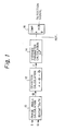
- Figure 1 shows a basic construction of a burst signal detection circuit according to an embodiment of the present invention.
- the circuit comprises a phase angle calculation unit 10, a deviation calculation unit 12, a variance parameter calculation unit 14 and a comparator 16.
- the phase angle calculation unit 10 calculates an angle of a phase of a received signal with a phase of a reference signal that has been used in the quadrature detection, according to the following formula:
- the deviation calculation unit 12 calculates a deviation ⁇ of the observed phase angle 0 from expectation ⁇ of the angle ⁇ , according to the following formula:
- the variance parameter calculation unit 14 calculates a parameter related to a variance of the observed phase angle, for example, ⁇ 2 .
- the comparator 16 compares the variance parameter output from the variance calculation unit 14 with a reference value, and outputs a detection signal if the variance parameter is smaller than the reference value.
- received signals distibute around the origin of coordinate axes I and Q within a circle A on a plane of orthogonal coordinate axes I and Q, and the angle 0 uniformly distributes within a range from 0° to 360°. If a signal, for example, a carrier recovery training signal of the burst signal exists, a vector V of the existing signal is added and then the received signal distributes within a circle B. Therefore, the angle 0 distributes within a range from ⁇ - 6 to 0 + 6 where 0 is an angle of the signal vector.
- the circuit of Fig. 1 detects existence of the signal utilizing the above difference in an extent of distribution of the angle 0 between the case where a signal exists and the case where signals do not exist.
- the burst signal can be detected in the circuit of Fig. 1 by using the angle of the signal vector or a moving average of the observed phase angle ⁇ as the expectation of ⁇ .
- ⁇ is the difference between two successive samples of the angle ⁇ and ⁇ is an expectation of the ⁇ .
- the difference ⁇ corresponds to an angular velocity of the variation of the angle ⁇ .
- the angle ⁇ varies at a constant angular velocity corresponding to the difference between the frequencies of the received signal and the reference signal. Therefore, a variance of the deviation ⁇ calculated using the formula (3) becomes smaller while a burst signal is received than while signals are not received.
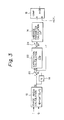
- Figure 3 shows a construction of a burst signal detection circuit according to the above principle.
- the output signal of the phase angle calculation unit 10 is delayed by one sample interval in a delay unit 18.
- the angular velocity ⁇ is calculated by subtracting the delayed phase angle from a current phase angle in a subtracter 20.
- An expectation calculation unit 22 calculates an expectation ⁇ of the angular velocity ⁇ e.
- the deviation a is calculated by subtracting the expectation ⁇ from an instantaneous value ⁇ in a subtracter 24.
- Figure 4 shows a detailed construction of the burst signal detection circuit of Fig. 3.
- the phase angle calculation unit 10 is realized by a read only memory (ROM) 26.
- ROM 26 has an address input connected to each bit of the digital baseband signals I and Q, and stores values of the phase angle 0 that have been calculated in advance according to the formula (1) in corresponding memory cells.
- the expectation calculation unit 22 is realized by a moving average calculation circuit consisting of a delay element 28, a subtracter 30, an adder 32, a delay element 34, and a divider 36.
- the delay element 28 delays input data by N sample intervals and the delay element 34 delays input data by one sample interval.
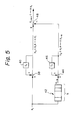
- the circuit consisting of the delay elements 28 and 34, the subtracter 30, and the adder 32 calculates a sum of recent N samples of input data. To explain this operation of the circuit, the circuit is equivalently modified as shown in Fig. 5.
- a circuit consisting of an adder 38 and a delay element 40 outputs a sum of i samples (xo + x 1 + ••• + x 1 ).
- a circuit consisting of delay elements 42 and 46 and an adder 44 outputs a sum of i - N samples (xo + x 1 + ••• + x i-N ), provided that N flip-flops constituting the delay element 42 are initially cleared to zero.
- a sum of recent N samples (x i-N+1 , + ••• + +x i ) is obtained in an output of the subtracter 48.
- the sum of the recent N samples of ⁇ is divided by N in the divider 36 to obtain a moving average ⁇ of ⁇ e. If N is 2 n , division in the divider 36 is realized by shifting n bits.
- the variation parameter calculation unit 14 is constituted by a multiplier 50 for calculating a square of the deviation 0 2 and a circuit for calculating a sum of the square ⁇ 2 .
- the multiplier 50 can be realized by a ROM similar to the ROM 26.
- the circuit for calculating E 0 2 is constituted by delay elements 52, 54, a subtracter 56 and an adder 58 which have the same construction as that for calculating the sum of recent N samples of ⁇ .
- the comparator 16 is realized by a digital comparactor 60.
- decision of existence of the burst signal is performed essentially not based on the amplitude of the received signal but based on the phase of the received signal. Therefore, fluctuation in amplitude of the received signal does not affect the decision, and the AGC can be operated to ensure the decision.
Landscapes
- Engineering & Computer Science (AREA)
- Computer Networks & Wireless Communication (AREA)
- Signal Processing (AREA)
- Digital Transmission Methods That Use Modulated Carrier Waves (AREA)
- Synchronisation In Digital Transmission Systems (AREA)
Applications Claiming Priority (2)
| Application Number | Priority Date | Filing Date | Title |
|---|---|---|---|
| JP267633/91 | 1991-10-16 | ||
| JP3267633A JP2848420B2 (ja) | 1991-10-16 | 1991-10-16 | バースト信号検出装置および方法 |
Publications (3)
| Publication Number | Publication Date |
|---|---|
| EP0537706A2 true EP0537706A2 (de) | 1993-04-21 |
| EP0537706A3 EP0537706A3 (en) | 1993-07-21 |
| EP0537706B1 EP0537706B1 (de) | 1998-01-07 |
Family
ID=17447394
Family Applications (1)
| Application Number | Title | Priority Date | Filing Date |
|---|---|---|---|
| EP92117538A Expired - Lifetime EP0537706B1 (de) | 1991-10-16 | 1992-10-14 | Verfahren und Schaltung zur Detektion des Vorhandenseins eines Burstsignals |
Country Status (5)
| Country | Link |
|---|---|
| US (1) | US5457710A (de) |
| EP (1) | EP0537706B1 (de) |
| JP (1) | JP2848420B2 (de) |
| CA (1) | CA2080323C (de) |
| DE (1) | DE69223901T2 (de) |
Cited By (4)
| Publication number | Priority date | Publication date | Assignee | Title |
|---|---|---|---|---|
| EP0827298A3 (de) * | 1996-09-02 | 2001-03-21 | Sony Corporation | Datenempfänger und Empfangsverfahren |
| EP0827299A3 (de) * | 1996-09-02 | 2001-03-21 | Sony Corporation | Datenempfänger und Empfangsverfahren mit Soft-Dekodierung |
| EP0866580A3 (de) * | 1997-03-18 | 2001-05-02 | Matsushita Electric Industrial Co., Ltd. | Fehlerrateschätzer für PSK Signale |
| US6324224B1 (en) | 1996-09-03 | 2001-11-27 | Sony Corporation | Apparatus and method for receiving data with bit insertion |
Families Citing this family (4)
| Publication number | Priority date | Publication date | Assignee | Title |
|---|---|---|---|---|
| US8724744B2 (en) * | 2005-08-19 | 2014-05-13 | General Instrument Corporation | Method and apparatus for wide dynamic range reduction |
| US8687748B2 (en) * | 2007-11-28 | 2014-04-01 | Mediatek Inc. | Radio frequency control for communication systems |
| US9413575B2 (en) | 2013-03-15 | 2016-08-09 | Echelon Corporation | Method and apparatus for multi-carrier modulation (MCM) packet detection based on phase differences |
| US9363128B2 (en) | 2013-03-15 | 2016-06-07 | Echelon Corporation | Method and apparatus for phase-based multi-carrier modulation (MCM) packet detection |
Family Cites Families (9)
| Publication number | Priority date | Publication date | Assignee | Title |
|---|---|---|---|---|
| US4466108A (en) * | 1981-10-06 | 1984-08-14 | Communications Satellite Corporation | TDMA/PSK Carrier synchronization without preamble |
| US4485448A (en) * | 1982-02-26 | 1984-11-27 | Sperry Corporation | Apparatus and method for detecting the onset of a frequency shift keyed signal |
| US4603300A (en) * | 1984-09-21 | 1986-07-29 | General Electric Company | Frequency modulation detector using digital signal vector processing |
| FR2583938A1 (fr) * | 1985-06-21 | 1986-12-26 | Labo Electronique Physique | Filtre numerique de quadrature et demodulateur de signal numerique module en frequence comprenant un tel filtre |
| DE3915779A1 (de) * | 1989-05-13 | 1990-11-15 | Telefunken Systemtechnik | Einrichtung zur erkennung phasengetasteter signale |
| CA2018855C (en) * | 1989-06-14 | 1993-09-21 | Shousei Yoshida | Burst demodulator for establishing carrier and clock timing from a sequence of alternating symbols |
| US5023940A (en) * | 1989-09-01 | 1991-06-11 | Motorola, Inc. | Low-power DSP squelch |
| JPH0771053B2 (ja) * | 1990-03-28 | 1995-07-31 | 松下電器産業株式会社 | バースト位置検出装置 |
| US5289391A (en) * | 1992-02-10 | 1994-02-22 | Aerometrics, Inc. | Method and apparatus for optimum signal burst detection |
-
1991
- 1991-10-16 JP JP3267633A patent/JP2848420B2/ja not_active Expired - Fee Related
-
1992
- 1992-10-09 CA CA002080323A patent/CA2080323C/en not_active Expired - Fee Related
- 1992-10-14 EP EP92117538A patent/EP0537706B1/de not_active Expired - Lifetime
- 1992-10-14 DE DE69223901T patent/DE69223901T2/de not_active Expired - Fee Related
- 1992-10-16 US US07/962,116 patent/US5457710A/en not_active Expired - Fee Related
Cited By (6)
| Publication number | Priority date | Publication date | Assignee | Title |
|---|---|---|---|---|
| EP0827298A3 (de) * | 1996-09-02 | 2001-03-21 | Sony Corporation | Datenempfänger und Empfangsverfahren |
| EP0827299A3 (de) * | 1996-09-02 | 2001-03-21 | Sony Corporation | Datenempfänger und Empfangsverfahren mit Soft-Dekodierung |
| US6327316B1 (en) | 1996-09-02 | 2001-12-04 | Sony Corporation | Data receiver using approximated bit metrics |
| US6381727B1 (en) | 1996-09-02 | 2002-04-30 | Sony Corporation | Apparatus and method for receiving data with bit insertion |
| US6324224B1 (en) | 1996-09-03 | 2001-11-27 | Sony Corporation | Apparatus and method for receiving data with bit insertion |
| EP0866580A3 (de) * | 1997-03-18 | 2001-05-02 | Matsushita Electric Industrial Co., Ltd. | Fehlerrateschätzer für PSK Signale |
Also Published As
| Publication number | Publication date |
|---|---|
| JPH05110611A (ja) | 1993-04-30 |
| DE69223901D1 (de) | 1998-02-12 |
| DE69223901T2 (de) | 1998-05-20 |
| CA2080323A1 (en) | 1993-04-17 |
| US5457710A (en) | 1995-10-10 |
| CA2080323C (en) | 1999-01-19 |
| EP0537706B1 (de) | 1998-01-07 |
| JP2848420B2 (ja) | 1999-01-20 |
| EP0537706A3 (en) | 1993-07-21 |
Similar Documents
| Publication | Publication Date | Title |
|---|---|---|
| EP0632606B1 (de) | Verfahren und Gerät zur Erstellung und zum Erhalten der Rahmensynchronisation in einer Satelliten Kommunikationsanordnung | |
| JP3118548B2 (ja) | ディジタル通信受信機用同期検波装置および同期方法 | |
| EP0125805A2 (de) | Bit-Fehler Detektionsschaltung für eine PSK-modulierte Trägerwelle | |
| US4457005A (en) | Digital coherent PSK demodulator and detector | |
| US5247544A (en) | Phase adjustment method and apparatus for use in a clock recovery circuit | |
| US6094463A (en) | Phaselock threshold correction | |
| JPH11177544A (ja) | 受信同期回路とこれを用いた受信機及びデジタル通信システム | |
| EP0537706A2 (de) | Verfahren und Schaltung zur Detektion eines Burstsignals | |
| EP0593015B1 (de) | Trägerphasenverriegelungsdetektor für PSK-Satellitensysteme | |
| US5412694A (en) | Data demodulator | |
| JP2912097B2 (ja) | 判断指向クロック回復システムを変更するための方法及び装置 | |
| US5677934A (en) | Multipath propagation compensation in a TDMA system | |
| US5793250A (en) | Phase demodulator selectively using a first or a second detector | |
| HK1002134B (en) | Digital demodulator for pi/4 - qpsk signals | |
| US6603349B2 (en) | Doppler learning phase lock loop for burst demodulator | |
| CN110098881B (zh) | 宽窄波束信号传输方法、装置及电子设备 | |
| JP2638294B2 (ja) | 自動利得制御回路 | |
| JPH0629942A (ja) | 自動利得制御回路 | |
| JP3041320B2 (ja) | Ss−tdma基準局装置 | |
| JPH01101040A (ja) | スペクトラム拡散受信機 | |
| Chalmers et al. | A digitally implemented preambleless demodulator for maritime and mobile data communications | |
| JPH06204961A (ja) | 同期語検出回路 | |
| JPH05236044A (ja) | 自動レベル制御装置 | |
| JPH05347521A (ja) | 自動利得制御回路 | |
| JPH04274634A (ja) | スロット・タイミング同期方式 |
Legal Events
| Date | Code | Title | Description |
|---|---|---|---|
| PUAI | Public reference made under article 153(3) epc to a published international application that has entered the european phase |
Free format text: ORIGINAL CODE: 0009012 |
|
| AK | Designated contracting states |
Kind code of ref document: A2 Designated state(s): DE FR GB |
|
| PUAL | Search report despatched |
Free format text: ORIGINAL CODE: 0009013 |
|
| AK | Designated contracting states |
Kind code of ref document: A3 Designated state(s): DE FR GB |
|
| RHK1 | Main classification (correction) |
Ipc: H04L 27/00 |
|
| 17P | Request for examination filed |
Effective date: 19930811 |
|
| 17Q | First examination report despatched |
Effective date: 19960208 |
|
| GRAG | Despatch of communication of intention to grant |
Free format text: ORIGINAL CODE: EPIDOS AGRA |
|
| GRAH | Despatch of communication of intention to grant a patent |
Free format text: ORIGINAL CODE: EPIDOS IGRA |
|
| GRAH | Despatch of communication of intention to grant a patent |
Free format text: ORIGINAL CODE: EPIDOS IGRA |
|
| GRAA | (expected) grant |
Free format text: ORIGINAL CODE: 0009210 |
|
| AK | Designated contracting states |
Kind code of ref document: B1 Designated state(s): DE FR GB |
|
| REF | Corresponds to: |
Ref document number: 69223901 Country of ref document: DE Date of ref document: 19980212 |
|
| ET | Fr: translation filed | ||
| PLBE | No opposition filed within time limit |
Free format text: ORIGINAL CODE: 0009261 |
|
| STAA | Information on the status of an ep patent application or granted ep patent |
Free format text: STATUS: NO OPPOSITION FILED WITHIN TIME LIMIT |
|
| 26N | No opposition filed | ||
| REG | Reference to a national code |
Ref country code: GB Ref legal event code: IF02 |
|
| PGFP | Annual fee paid to national office [announced via postgrant information from national office to epo] |
Ref country code: FR Payment date: 20031003 Year of fee payment: 12 |
|
| PGFP | Annual fee paid to national office [announced via postgrant information from national office to epo] |
Ref country code: GB Payment date: 20031008 Year of fee payment: 12 |
|
| PGFP | Annual fee paid to national office [announced via postgrant information from national office to epo] |
Ref country code: DE Payment date: 20031023 Year of fee payment: 12 |
|
| PG25 | Lapsed in a contracting state [announced via postgrant information from national office to epo] |
Ref country code: GB Free format text: LAPSE BECAUSE OF NON-PAYMENT OF DUE FEES Effective date: 20041014 |
|
| PG25 | Lapsed in a contracting state [announced via postgrant information from national office to epo] |
Ref country code: DE Free format text: LAPSE BECAUSE OF NON-PAYMENT OF DUE FEES Effective date: 20050503 |
|
| GBPC | Gb: european patent ceased through non-payment of renewal fee |
Effective date: 20041014 |
|
| PG25 | Lapsed in a contracting state [announced via postgrant information from national office to epo] |
Ref country code: FR Free format text: LAPSE BECAUSE OF NON-PAYMENT OF DUE FEES Effective date: 20050630 |
|
| REG | Reference to a national code |
Ref country code: FR Ref legal event code: ST |