EP0537730A2 - Sonnenzelle - Google Patents
Sonnenzelle Download PDFInfo
- Publication number
- EP0537730A2 EP0537730A2 EP92117612A EP92117612A EP0537730A2 EP 0537730 A2 EP0537730 A2 EP 0537730A2 EP 92117612 A EP92117612 A EP 92117612A EP 92117612 A EP92117612 A EP 92117612A EP 0537730 A2 EP0537730 A2 EP 0537730A2
- Authority
- EP
- European Patent Office
- Prior art keywords
- solar cell
- electrode
- semiconductor layer
- photoelectric conversion
- cell according
- Prior art date
- Legal status (The legal status is an assumption and is not a legal conclusion. Google has not performed a legal analysis and makes no representation as to the accuracy of the status listed.)
- Granted
Links
Images



Classifications
-
- H—ELECTRICITY
- H10—SEMICONDUCTOR DEVICES; ELECTRIC SOLID-STATE DEVICES NOT OTHERWISE PROVIDED FOR
- H10F—INORGANIC SEMICONDUCTOR DEVICES SENSITIVE TO INFRARED RADIATION, LIGHT, ELECTROMAGNETIC RADIATION OF SHORTER WAVELENGTH OR CORPUSCULAR RADIATION
- H10F10/00—Individual photovoltaic cells, e.g. solar cells
- H10F10/10—Individual photovoltaic cells, e.g. solar cells having potential barriers
- H10F10/17—Photovoltaic cells having only PIN junction potential barriers
-
- H—ELECTRICITY
- H10—SEMICONDUCTOR DEVICES; ELECTRIC SOLID-STATE DEVICES NOT OTHERWISE PROVIDED FOR
- H10F—INORGANIC SEMICONDUCTOR DEVICES SENSITIVE TO INFRARED RADIATION, LIGHT, ELECTROMAGNETIC RADIATION OF SHORTER WAVELENGTH OR CORPUSCULAR RADIATION
- H10F77/00—Constructional details of devices covered by this subclass
- H10F77/20—Electrodes
- H10F77/206—Electrodes for devices having potential barriers
- H10F77/211—Electrodes for devices having potential barriers for photovoltaic cells
-
- Y—GENERAL TAGGING OF NEW TECHNOLOGICAL DEVELOPMENTS; GENERAL TAGGING OF CROSS-SECTIONAL TECHNOLOGIES SPANNING OVER SEVERAL SECTIONS OF THE IPC; TECHNICAL SUBJECTS COVERED BY FORMER USPC CROSS-REFERENCE ART COLLECTIONS [XRACs] AND DIGESTS
- Y02—TECHNOLOGIES OR APPLICATIONS FOR MITIGATION OR ADAPTATION AGAINST CLIMATE CHANGE
- Y02E—REDUCTION OF GREENHOUSE GAS [GHG] EMISSIONS, RELATED TO ENERGY GENERATION, TRANSMISSION OR DISTRIBUTION
- Y02E10/00—Energy generation through renewable energy sources
- Y02E10/50—Photovoltaic [PV] energy
- Y02E10/547—Monocrystalline silicon PV cells
-
- Y—GENERAL TAGGING OF NEW TECHNOLOGICAL DEVELOPMENTS; GENERAL TAGGING OF CROSS-SECTIONAL TECHNOLOGIES SPANNING OVER SEVERAL SECTIONS OF THE IPC; TECHNICAL SUBJECTS COVERED BY FORMER USPC CROSS-REFERENCE ART COLLECTIONS [XRACs] AND DIGESTS
- Y02—TECHNOLOGIES OR APPLICATIONS FOR MITIGATION OR ADAPTATION AGAINST CLIMATE CHANGE
- Y02E—REDUCTION OF GREENHOUSE GAS [GHG] EMISSIONS, RELATED TO ENERGY GENERATION, TRANSMISSION OR DISTRIBUTION
- Y02E10/00—Energy generation through renewable energy sources
- Y02E10/50—Photovoltaic [PV] energy
- Y02E10/548—Amorphous silicon PV cells
Definitions
- the present invention relates to a solar cell for use as a power supply to a variety of electronic equipments or a power source for power plant. More particularly, the invention relates to a solar cell having its electrode structure improved and excellent in the environment proof. Also, it relates to a solar cell which has a cheap, flexible and durable grid.
- the solar cell has been expected from all over the world as a reproducible, inexhaustible clean energy.
- three types of solar cell have been well known; single crystal silicon type, polycrystalline silicon type, and amorphous silicon type.
- An amorphous silicon type solar cell has excellent characteristics such as the thin film operation ability by virtue of its easy realization of large area or a great light absorption coefficient, unlike the crystal type solar cell, though it is interior in the conversion efficiency to the crystal type solar cell, and thus the amorphous silicon type solar cell is expected as one of the promising solar cells.
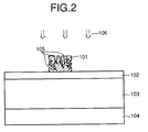
- FIG. 2 An example of the conventional amorphous silicon type solar cell is shown in Fig. 2.
- a photoelectric conversion semiconductor layer 103 made of amorphous silicon is formed on an electric conductive substratum 104, and a transparent electric conductive layer 102 also useful as an anti-reflection layer is formed thereon.
- On the transparent electric conductive layer is formed a grid electrode for collector 101. If light 106 is incident on the photoelectric conversion layer 103 from the grid electrode 101, as shown in Fig.
- the photoelectric conversion layer 103 contains at least one or more pin or pn junctions, with the p side acting as the anode and the n side as the cathode.
- the grid electrode is constituted of a conductive paste composed of silver 80wt% and phenolic resin 20wt%, but it is poor in durability and the gap volume (as shown at 105 in Fig. 2) may increase with the time.
- the gap volume (as shown at 105 in Fig. 2) may increase with the time.
- the solar cell having an output of several W or greater is used outdoors. Therefore, the so-called environment proof characteristics for the temperature and the humidity are required.
- conductive base substance such as silver or the like (as shown with Ag2O in Fig. 3) contained in the grid electrode may solve out by the permeation of water (as shown with Ag2O in Fig. 3) and by the photoelectromotive force of the substance so as to diffuse through defective portions such as pinholes or exfoliations, causing a short-circuit between the positive and negative electrodes of the solar cell, and thereby greatly decreasing the conversion efficiency.
- an object of the present invention is to provide a solar cell which is high in the environment proof and unlikely to degrade in the conversion efficiency.
- the above object of the present invention can be accomplished by a solar cell having a photoelectric conversion semiconductor layer and an electrode made of a material containing a conductive base substance and a resin electrically connected to the photoelectric conversion semiconductor layer, wherein the volume of gaps having a diameter of 0.1 ⁇ m or greater among gaps existing in the electrode is 0.04 cc/g or less.
- water content is prevented from entering gaps existing in the electrode to erode and break the electrode, so that the excellent photoelectric conversion efficiency of solar cell can be maintained for a long term.
- the photoelectric conversion semiconductor layer for use in the present invention may be a single crystal semiconductor layer, a polycrystal semiconductor layer or amorphous semiconductor layer as a non-single crystal semiconductor layer, or a crystallite semiconductor layer.
- Specific examples include silicon, germanium, carbon, silicon germanium, silicon carbide, CdSe, CdSeTe, CdTeAs, ZnSe, GaAs or the like in the above crystal structure.
- pn junction, pin junction, Schottky junction, hetero junction or the like is formed, using such a photoelectric conversion semiconductor layer.
- the electrode for use in the present invention is disposed directly or via another layer interposed therebetween on at least one face of the above photoelectric conversion semiconductor layer.
- the electrode for use in the present invention will be described below, but to facilitate the understanding of the contents of the art, an instance of the solar cell according to the present invention will be described in which amorphous silicon deposited on the conductive substratum is used as the photoelectric conversion semiconductor layer.
- An amorphous silicon layer having at least one pin junction is formed on a flat conductive substratum by plasma CVD using a silane gas.
- the conductive substratum may be a plate or sheet substratum of stainless, aluminum, copper, or titanium, or a carbon sheet or the like. Also, the substratum may be a resin substratum having metal or the like deposited thereon.
- a transparent conductive layer composed of indium oxide, tin oxide or the like is formed by vapor deposition, spraying, or the like.
- a conductive paste containing a conductive base substance and a resin is applied on the transparent conductive layer by screen printing or relief printing, and cured at a temperature of 100 to 200°C, whereby a grid electrode for collector is attached.
- a conductive paste containing a conductive base substance and a resin is applied on the transparent conductive layer by screen printing or relief printing, and cured at a temperature of 100 to 200°C, whereby a grid electrode for collector is attached.
- the solar cell of the present invention can be constituted by using a paste meeting the above viewpoints found by the present inventor.
- the conductive paste contains a solvent such as carhydro-acetate, butylcellulobuzo-acetate or polyhydric alcohol or the like, but this solvent will increase the gap volume in the grid, and is preferably at least in quantity as possible and most preferably a solventless type paste.
- the conductive base substance examples include silver, silver-palladium alloy, a mixture of silver and carbon, copper, nickel, aluminum, gold and a mixture thereof.
- the conductive base substance is preferably contained at 70 wt%, and more preferably at 75 wt% or greater.
- the resin include urethan type, epoxy type, polyimide type, polyester type, phenol type, vinyl type, acrylic type or the like. Particularly, the epoxy type is most preferable from the view-point of the waterproof and the economy.
- the curing temperature of the conductive paste is preferably as high as possible in order to raise the density of crosslinking for the resin, but since too high temperature will burn the resin to thereby increase the gap volume, it should be appropriately selected and set within the range of accomplishing the objects of the present invention.
- the urethan type or epoxy type resin it is desirably 200°C or less.
- Fig. 1 is a typical view for explaining the solar cell according to an embodiment of the present invention.
- a collector electrode 101 is provided on a photoelectric conversion semiconductor layer 103 and a transparent conductive layer 102 sequentially formed on a substratum 104.
- 201 shows a relative large gap having a diameter of, for example 0.1 ⁇ m or greater
- 202 shows a relatively small gap having a diameter of, for example, less than 0.1 ⁇ m.
- the shape of gap is such that the shape of opening on the electrode surface and the shape of gap in cross section within the electrode may be any one ranging from a polygon to a star such as a circle, an ellipse, a triangle and a quadrangle. And each gap may or may not communicate to one another.
- the gap diameter and the gap volume as defined in the present invention can be obtained in the following way.
- the liquid producing no wetting which indicates a contact angle from 90° to 180° to most substances, will not enter the pore unless force-fully pressed, and enter correctly the pore in accordance with the applied pressure and the size (diameter) of pore, so that the volume of mercury permeating the pore can be measured by the diameter of pore and the work used to force mercury into the pore as the function of the applied pressure. With this mercury porosimetry, the diameter and the volume of gap in the grid electrode can be obtained.
- the gap volume having a gap diameter of 0.1 ⁇ m or greater in the electrode is 0.04 cc/g or less, and more preferably 0.02 cc/g or less, water content is difficult to reach the conductive base substance, whereby the reaction of the formula (A), and thus the creation of silver ions are prevented, making no short-circuit, so that the conversion efficinecy is not degraded.
- Fig. 7 shows the relation between the gap volume and the leakage current increment rate per hour, which indicated that the leakage current increament rate per hour is particularly small or excellent when the gap volume is 0.04 cc/g or less.
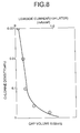
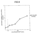
- Fig. 8 shows the leakage current after ten hours, with the gap volume being 0.02 cc/g, when a forward bias is applied under the conditions of high temperature and high humidity, and the concentration (density) of chlorine is changed, and Fig. 9 shows a minuter result thereof.
- a solar cell having a photoelectric conversion semiconductor layer and an electrode made of a material containing a conductive base substance and a resin electrically connected to the photoelectric conversion semiconductor layer, in which the short-circuit between solar cell electrodes due to water content permeation can be prevented, and the environment proof is excellent, owing to the fact: that the volume of gaps having a diameter of 0.1 ⁇ m or greater among gaps existing in the electrode is 0.04 cc/g or less, or that the volume of gaps having a diameter of 20 ⁇ or greater among gaps existing in the electrode is 0.04 cc/g or less, or that the ratio of weight of the conductive base substance in the grid electrode is 70% or greater, or that the resin is urethan type, epoxy type or polyimide type, or that the concentration of chlorine contained in the electrode as impurities is 0.1 wt% or less.
- the grid Since a mixture of resin and conductive base substance is used for the grid, the grid is attached at a low temperature, so that the solar cell can be fabricated cheaply.
- the grid having a resin contained is bendable and durable to mechanical impact, it is possible to provide a flexible and durable solar cell.
- Fig. 1 is a solar cell.
- Fig. 2 is a conventional solar cell.
- Fig. 3 is an explanation view showing the principle of the degradation in the conventional solar cell.
- Fig. 4 shows a result of Example 1.
- Fig. 5 shows a result of Example 2.
- Fig. 6 is a view showing the improvement in the gap volume with decreasing weight of solvent.
- Fig. 7 is a view showing the decreasing leakage current increment rate per hour with the improved gap volume.
- Fig. 8 is a view showing the improvement in the leakage current with decreasing content of chlorine concentration.
- Fig. 9 is a view showing the improvement in the leakage current with decreasing content of chlorine concentration.
- a plurality of photoelectric conversion layers composed of amorphous silicon were deposited on a stainless substratum having a thickness of 8MIL and an area of 16 cm2 by plasma CVD, and a transparent conductive layer composed of an indium oxide was adhered thereto by sputtering.
- a conductive paste composed of an urethan type resin and silver particulates (conductive base substance 70 wt%, solvent 18 wt%, resin 12 wt%) was screen printed, and cured at a temperature of 130°C for one hour to make up a solar cell of the present invention.
- Total volume of gaps having a diameter of 20 ⁇ or greater in the grid electrode measured by mercury porosimetry was 0.036 cc/g, while the volume of gaps having a diameter of 1 ⁇ m or greater was 0.018 cc/g.
- a forward bias of 1.2V was applied to this solar cell under the conditions at a high temperature of 85°C and a high humidity of 85%RH to appropriately measure the leakage current flowing within the solar cell.
- the forward bias was applied to simulate the operation state.
- the leakage current increment rate was 0.2 mA/cm2 or less per hour, and it could be found that the elution of silver was greatly decreased.
- Fig. 4 The longitudinal axis of Fig. 4 indicates the leakage current value per unit area, and the transversal axis indicates the time.
- the leakage current increment in this example is indicated by the solid line A.
- the dotted line indicates the leakage current increment of comparative example 1 as will be described later.
- a conductive paste composed of a polyester type resin and silver particulates (conductive base substance 70wt%, solvent 25wt%, resin 5 wt%).
- Total volume of gaps having a diameter of 20 ⁇ or greater measured in the same way as example 1 was 0.065 cc/g, while the volume of gaps having a diameter of 0.1 ⁇ m or greater was 0.046 cc/g.
- the leakage current increment rate reached 2.0 mA/cm2 per hour.
- the same test as in example 1 was performed using a conductive paste composed of a vinyl type resin and silver particulates (conductive base substance 70 wt%, solvent 22 wt%, resin 8 wt%).
- Total volume of gaps having a diameter of 20 ⁇ or greater was 0.060 cc/g, while the volume of gaps having a diameter of 0.1 ⁇ m or greater was 0.041 cc/g.
- the leakage current increment rate was 1.8 mA/cm2 per hour.
- a solar cell was fabricated using a conductive paste composed of an epoxy type resin and silver particulates (conductive base substance 80 wt%, solventless).
- the curing condition was 150°C for three hours.
- Total volume of gaps having a diameter of 20 ⁇ or greater was 0.018 cc/g, while the volume of gaps having a diameter of 1 ⁇ m or greater was 0.030 cc/g. This is due to the fact that no solvent is contained and the epoxy type resin has a very small amount of volatile matters arising in crosslinking.
- a forward bias was applied to this solar cell under the conditions at a high temperature of 85°C and a high humidity of 85%RH to measure the leakage current increment.
- FIG. 5 This result is shown in Fig. 5 together with that of the comparative example 1.
- the solid line A indicates the leakage current in this example
- the dotted line B indicates the leakage current of the comparative example 1.
- the leakage current increment rate was 0.03 mA/cm2 per hour, which was above 1/100 that of the comparative example. It is indicated that this value is about 1/10 that of the example 1, and a great effect can be provided by using such conductive paste having a small amount of volatile matters arising in curing.
- tandem-type amorphous solar cells A and B were fabricated in the same method as in example 1.
- total volume of gaps having a diameter of 20 ⁇ or greater was 0.016 cc/g in A and 0.018 cc/g in B.
- the volume of gaps having a diameter of 1 ⁇ m or greater was almost the same value for both A and B, i.e., 0.003 cc/g.
- the concentration of chlorine in the electrode was 0.01 wt% in A, but it could not be detected in B.
- the measurement method was ion exchange chromatography. The detection limit of used equipment was 0.001 wt%.
- the present invention can provide a solar cell excellent in the environment proof so that the short-circuit between solar cell electrodes due to water permeation can be prevented using a grid electrode in which the volume of gaps having a diameter of 0.1 ⁇ m or greater is 0.04 cc/g or less.
- the grid can be attached at a low temperature because of the use of a mixture of a resin and a conductive base substance in the grid, whereby the solar cell can be fabricated cheaply.
- the grid having the resin contained is bendable and durable to mechanical impact, it is possible to provide a flexible and durable solar cell.
- a solar cell has a photoelectric conversion semiconductor layer and an electrode made of a material containing a conductive base substance and a resin electrically connected to the photoelectric conversion semiconductor layer, wherein the volume of gaps having a diameter of 0.1 ⁇ m or greater among gaps existing in the electrode is 0.04 cc/g or less.
Landscapes
- Photovoltaic Devices (AREA)
Applications Claiming Priority (3)
| Application Number | Priority Date | Filing Date | Title |
|---|---|---|---|
| JP271033/91 | 1991-10-18 | ||
| JP27103391 | 1991-10-18 | ||
| JP27103391A JP3156973B2 (ja) | 1991-10-18 | 1991-10-18 | 太陽電池 |
Related Child Applications (1)
| Application Number | Title | Priority Date | Filing Date |
|---|---|---|---|
| EP99107885.8 Division-Into | 1999-04-21 |
Publications (3)
| Publication Number | Publication Date |
|---|---|
| EP0537730A2 true EP0537730A2 (de) | 1993-04-21 |
| EP0537730A3 EP0537730A3 (en) | 1993-10-06 |
| EP0537730B1 EP0537730B1 (de) | 2002-01-30 |
Family
ID=17494470
Family Applications (1)
| Application Number | Title | Priority Date | Filing Date |
|---|---|---|---|
| EP92117612A Expired - Lifetime EP0537730B1 (de) | 1991-10-18 | 1992-10-15 | Sonnenzelle |
Country Status (5)
| Country | Link |
|---|---|
| US (2) | US5318638A (de) |
| EP (1) | EP0537730B1 (de) |
| JP (1) | JP3156973B2 (de) |
| AU (1) | AU647675B2 (de) |
| DE (1) | DE69232390T2 (de) |
Cited By (1)
| Publication number | Priority date | Publication date | Assignee | Title |
|---|---|---|---|---|
| EP1542290A1 (de) * | 2003-12-10 | 2005-06-15 | Sanyo Electric Co., Ltd. | Photovoltaisches Bauelement |
Families Citing this family (17)
| Publication number | Priority date | Publication date | Assignee | Title |
|---|---|---|---|---|
| US4357164A (en) * | 1979-12-11 | 1982-11-02 | Sakata Shokai, Ltd. | Ink composition for waterless lithography and methods of printing therefrom |
| JP2938634B2 (ja) * | 1991-10-08 | 1999-08-23 | キヤノン株式会社 | 太陽電池モジュール |
| US5340409A (en) * | 1992-04-23 | 1994-08-23 | Canon Kabushiki Kaisha | Photovoltaic element and method for forming the same |
| US5428249A (en) * | 1992-07-15 | 1995-06-27 | Canon Kabushiki Kaisha | Photovoltaic device with improved collector electrode |
| US20030148024A1 (en) * | 2001-10-05 | 2003-08-07 | Kodas Toivo T. | Low viscosity precursor compositons and methods for the depositon of conductive electronic features |
| US20030108664A1 (en) * | 2001-10-05 | 2003-06-12 | Kodas Toivo T. | Methods and compositions for the formation of recessed electrical features on a substrate |
| US6951666B2 (en) * | 2001-10-05 | 2005-10-04 | Cabot Corporation | Precursor compositions for the deposition of electrically conductive features |
| JP4763237B2 (ja) * | 2001-10-19 | 2011-08-31 | キャボット コーポレイション | 基板上に導電性電子部品を製造する方法 |
| EP2032291A2 (de) * | 2006-06-19 | 2009-03-11 | Cabot Corporation | Metallhaltige nanopartikel, ihre synthese und verwendung |
| US20090266399A1 (en) * | 2008-04-28 | 2009-10-29 | Basol Bulent M | Metallic foil substrate and packaging technique for thin film solar cells and modules |
| US20090266398A1 (en) * | 2008-04-28 | 2009-10-29 | Burak Metin | Method and Apparatus to Form Back Contacts to Flexible CIGS Solar Cells |
| US8207012B2 (en) * | 2008-04-28 | 2012-06-26 | Solopower, Inc. | Method and apparatus for achieving low resistance contact to a metal based thin film solar cell |
| US20100180940A1 (en) * | 2009-01-20 | 2010-07-22 | Weihong Cui | Photovoltaic Module With Stabilized Polymer |
| WO2012124463A1 (ja) * | 2011-03-17 | 2012-09-20 | 三洋電機株式会社 | 太陽電池及び太陽電池モジュール |
| US20130240009A1 (en) * | 2012-03-18 | 2013-09-19 | The Boeing Company | Metal Dendrite-free Solar Cell |
| WO2013140622A1 (ja) * | 2012-03-23 | 2013-09-26 | 三洋電機株式会社 | 太陽電池モジュール |
| US20130263921A1 (en) * | 2012-04-10 | 2013-10-10 | Lauren Plavisch | Electronic Device and Corrosion Resistant Electrode Stack Therein |
Family Cites Families (12)
| Publication number | Priority date | Publication date | Assignee | Title |
|---|---|---|---|---|
| US4084985A (en) * | 1977-04-25 | 1978-04-18 | The United States Of America As Represented By The Administrator Of The National Aeronautics And Space Administration | Method for producing solar energy panels by automation |
| JPS59167057A (ja) * | 1983-03-12 | 1984-09-20 | Agency Of Ind Science & Technol | シリコン半導体電極 |
| JPS59167056A (ja) * | 1983-03-12 | 1984-09-20 | Agency Of Ind Science & Technol | シリコン半導体電極 |
| JPS59168669A (ja) * | 1983-03-16 | 1984-09-22 | Hitachi Ltd | 電極用ペースト材料 |
| JPS63185071A (ja) * | 1987-01-27 | 1988-07-30 | Matsushita Electric Ind Co Ltd | 非晶質太陽電池 |
| US4968354A (en) * | 1987-11-09 | 1990-11-06 | Fuji Electric Co., Ltd. | Thin film solar cell array |
| JPH0658968B2 (ja) * | 1987-11-09 | 1994-08-03 | 富士電機株式会社 | 薄膜太陽電池の製造方法 |
| JPH01149484A (ja) * | 1987-12-04 | 1989-06-12 | Sanyo Electric Co Ltd | 光起電力装置 |
| DE3804831C1 (en) * | 1988-02-17 | 1989-07-20 | Degussa Ag, 6000 Frankfurt, De | Electroconductive coating composition for the contacting of solar cells |
| JP2698401B2 (ja) * | 1988-10-26 | 1998-01-19 | 富士電機株式会社 | 薄膜光電変換素子 |
| JPH02298079A (ja) * | 1989-05-12 | 1990-12-10 | Fuji Electric Co Ltd | 薄膜太陽電池の製造方法 |
| JPH0338069A (ja) * | 1989-07-04 | 1991-02-19 | Fuji Electric Co Ltd | 薄膜太陽電池 |
-
1991
- 1991-10-18 JP JP27103391A patent/JP3156973B2/ja not_active Expired - Lifetime
-
1992
- 1992-10-07 US US07/957,150 patent/US5318638A/en not_active Expired - Lifetime
- 1992-10-15 EP EP92117612A patent/EP0537730B1/de not_active Expired - Lifetime
- 1992-10-15 DE DE69232390T patent/DE69232390T2/de not_active Expired - Fee Related
- 1992-10-16 AU AU27098/92A patent/AU647675B2/en not_active Ceased
-
1994
- 1994-03-18 US US08/214,547 patent/US5393695A/en not_active Expired - Lifetime
Cited By (2)
| Publication number | Priority date | Publication date | Assignee | Title |
|---|---|---|---|---|
| EP1542290A1 (de) * | 2003-12-10 | 2005-06-15 | Sanyo Electric Co., Ltd. | Photovoltaisches Bauelement |
| US7947895B2 (en) | 2003-12-10 | 2011-05-24 | Sanyo Electric Co., Ltd. | Photovoltaic device |
Also Published As
| Publication number | Publication date |
|---|---|
| DE69232390D1 (de) | 2002-03-14 |
| DE69232390T2 (de) | 2002-07-11 |
| AU2709892A (en) | 1993-04-22 |
| JPH05110124A (ja) | 1993-04-30 |
| AU647675B2 (en) | 1994-03-24 |
| EP0537730B1 (de) | 2002-01-30 |
| JP3156973B2 (ja) | 2001-04-16 |
| US5393695A (en) | 1995-02-28 |
| EP0537730A3 (en) | 1993-10-06 |
| US5318638A (en) | 1994-06-07 |
Similar Documents
| Publication | Publication Date | Title |
|---|---|---|
| EP0537730B1 (de) | Sonnenzelle | |
| US8907206B2 (en) | Multi-junction solar cell devices | |
| US6132585A (en) | Semiconductor element and method and apparatus for fabricating the same | |
| US6051778A (en) | Electrode structure, process production thereof and photo-electricity generating device including the electrode | |
| US4084985A (en) | Method for producing solar energy panels by automation | |
| US5527717A (en) | Method of making solar cell module with improved weathering characteristics | |
| US5785768A (en) | Photo cells, photo cell arrays, and electrolytic devices using these cells and arrays | |
| US4647711A (en) | Stable front contact current collector for photovoltaic devices and method of making same | |
| DE102006042617A1 (de) | Lokale Heterostrukturkontakte | |
| WO1982002459A1 (en) | Methods and apparatus for forming thin-film heterojunction solar cells from i-iii-vi2 chalcopyrite compounds,and solar cells produced thereby | |
| JPH07106617A (ja) | 透明電極及びその形成方法並びに該透明電極を用いた太陽電池 | |
| Zhang et al. | Large area, concentrator buried contact solar cells | |
| JP4266840B2 (ja) | 太陽電池モジュール | |
| US4595791A (en) | Thin-film photovoltaic devices incorporating current collector grid and method of making | |
| Wirth | Photovoltaic module technology | |
| JP3078936B2 (ja) | 太陽電池 | |
| AU646773B2 (en) | Photovoltaic element and method of forming the same | |
| Soliman et al. | Reactively sputtered TiO2 electrodes from metallic targets for water electrolysis using solar energy | |
| KR810001314B1 (ko) | 비결정 실리콘 활성영역을 갖는 반도체 장치 | |
| JP3078951B2 (ja) | 光起電力素子 | |
| Frisson et al. | Screen printed metallization of silicon solar cells | |
| Williams | Gold in solar cells: A review of current work | |
| JPH0794767A (ja) | 光電変換素子 | |
| JP3314958B2 (ja) | 半導体光エネルギー変換装置 | |
| JP2706948B2 (ja) | 光センサー |
Legal Events
| Date | Code | Title | Description |
|---|---|---|---|
| PUAI | Public reference made under article 153(3) epc to a published international application that has entered the european phase |
Free format text: ORIGINAL CODE: 0009012 |
|
| AK | Designated contracting states |
Kind code of ref document: A2 Designated state(s): CH DE FR GB IT LI |
|
| PUAL | Search report despatched |
Free format text: ORIGINAL CODE: 0009013 |
|
| AK | Designated contracting states |
Kind code of ref document: A3 Designated state(s): CH DE FR GB IT LI |
|
| 17P | Request for examination filed |
Effective date: 19940221 |
|
| 17Q | First examination report despatched |
Effective date: 19950222 |
|
| APAB | Appeal dossier modified |
Free format text: ORIGINAL CODE: EPIDOS NOAPE |
|
| APAB | Appeal dossier modified |
Free format text: ORIGINAL CODE: EPIDOS NOAPE |
|
| APAD | Appeal reference recorded |
Free format text: ORIGINAL CODE: EPIDOS REFNE |
|
| APAD | Appeal reference recorded |
Free format text: ORIGINAL CODE: EPIDOS REFNE |
|
| APAB | Appeal dossier modified |
Free format text: ORIGINAL CODE: EPIDOS NOAPE |
|
| GRAG | Despatch of communication of intention to grant |
Free format text: ORIGINAL CODE: EPIDOS AGRA |
|
| GRAG | Despatch of communication of intention to grant |
Free format text: ORIGINAL CODE: EPIDOS AGRA |
|
| GRAG | Despatch of communication of intention to grant |
Free format text: ORIGINAL CODE: EPIDOS AGRA |
|
| GRAH | Despatch of communication of intention to grant a patent |
Free format text: ORIGINAL CODE: EPIDOS IGRA |
|
| GRAH | Despatch of communication of intention to grant a patent |
Free format text: ORIGINAL CODE: EPIDOS IGRA |
|
| GRAA | (expected) grant |
Free format text: ORIGINAL CODE: 0009210 |
|
| REG | Reference to a national code |
Ref country code: GB Ref legal event code: IF02 |
|
| AK | Designated contracting states |
Kind code of ref document: B1 Designated state(s): CH DE FR GB IT LI |
|
| REG | Reference to a national code |
Ref country code: CH Ref legal event code: EP |
|
| REG | Reference to a national code |
Ref country code: CH Ref legal event code: NV Representative=s name: BOVARD AG PATENTANWAELTE |
|
| REF | Corresponds to: |
Ref document number: 69232390 Country of ref document: DE Date of ref document: 20020314 |
|
| ET | Fr: translation filed | ||
| PLBE | No opposition filed within time limit |
Free format text: ORIGINAL CODE: 0009261 |
|
| STAA | Information on the status of an ep patent application or granted ep patent |
Free format text: STATUS: NO OPPOSITION FILED WITHIN TIME LIMIT |
|
| 26N | No opposition filed | ||
| PGFP | Annual fee paid to national office [announced via postgrant information from national office to epo] |
Ref country code: DE Payment date: 20041007 Year of fee payment: 13 |
|
| PGFP | Annual fee paid to national office [announced via postgrant information from national office to epo] |
Ref country code: GB Payment date: 20041013 Year of fee payment: 13 |
|
| PGFP | Annual fee paid to national office [announced via postgrant information from national office to epo] |
Ref country code: CH Payment date: 20041015 Year of fee payment: 13 |
|
| APAH | Appeal reference modified |
Free format text: ORIGINAL CODE: EPIDOSCREFNO |
|
| PGFP | Annual fee paid to national office [announced via postgrant information from national office to epo] |
Ref country code: FR Payment date: 20051010 Year of fee payment: 14 |
|
| PG25 | Lapsed in a contracting state [announced via postgrant information from national office to epo] |
Ref country code: IT Free format text: LAPSE BECAUSE OF NON-PAYMENT OF DUE FEES Effective date: 20051015 Ref country code: GB Free format text: LAPSE BECAUSE OF NON-PAYMENT OF DUE FEES Effective date: 20051015 |
|
| PG25 | Lapsed in a contracting state [announced via postgrant information from national office to epo] |
Ref country code: LI Free format text: LAPSE BECAUSE OF NON-PAYMENT OF DUE FEES Effective date: 20051031 Ref country code: CH Free format text: LAPSE BECAUSE OF NON-PAYMENT OF DUE FEES Effective date: 20051031 |
|
| PG25 | Lapsed in a contracting state [announced via postgrant information from national office to epo] |
Ref country code: DE Free format text: LAPSE BECAUSE OF NON-PAYMENT OF DUE FEES Effective date: 20060503 |
|
| REG | Reference to a national code |
Ref country code: CH Ref legal event code: PL |
|
| GBPC | Gb: european patent ceased through non-payment of renewal fee |
Effective date: 20051015 |
|
| REG | Reference to a national code |
Ref country code: FR Ref legal event code: ST Effective date: 20070629 |
|
| PG25 | Lapsed in a contracting state [announced via postgrant information from national office to epo] |
Ref country code: FR Free format text: LAPSE BECAUSE OF NON-PAYMENT OF DUE FEES Effective date: 20061031 |