EP0539015A1 - Laser à semi-conducteur à longueurs d'ondes multiples - Google Patents
Laser à semi-conducteur à longueurs d'ondes multiples Download PDFInfo
- Publication number
- EP0539015A1 EP0539015A1 EP92308463A EP92308463A EP0539015A1 EP 0539015 A1 EP0539015 A1 EP 0539015A1 EP 92308463 A EP92308463 A EP 92308463A EP 92308463 A EP92308463 A EP 92308463A EP 0539015 A1 EP0539015 A1 EP 0539015A1
- Authority
- EP
- European Patent Office
- Prior art keywords
- laser
- quantum
- region
- level
- quantum well
- Prior art date
- Legal status (The legal status is an assumption and is not a legal conclusion. Google has not performed a legal analysis and makes no representation as to the accuracy of the status listed.)
- Granted
Links
Images






Classifications
-
- B—PERFORMING OPERATIONS; TRANSPORTING
- B82—NANOTECHNOLOGY
- B82Y—SPECIFIC USES OR APPLICATIONS OF NANOSTRUCTURES; MEASUREMENT OR ANALYSIS OF NANOSTRUCTURES; MANUFACTURE OR TREATMENT OF NANOSTRUCTURES
- B82Y20/00—Nanooptics, e.g. quantum optics or photonic crystals
-
- H—ELECTRICITY
- H01—ELECTRIC ELEMENTS
- H01S—DEVICES USING THE PROCESS OF LIGHT AMPLIFICATION BY STIMULATED EMISSION OF RADIATION [LASER] TO AMPLIFY OR GENERATE LIGHT; DEVICES USING STIMULATED EMISSION OF ELECTROMAGNETIC RADIATION IN WAVE RANGES OTHER THAN OPTICAL
- H01S3/00—Lasers, i.e. devices using stimulated emission of electromagnetic radiation in the infrared, visible or ultraviolet wave range
- H01S3/10—Controlling the intensity, frequency, phase, polarisation or direction of the emitted radiation, e.g. switching, gating, modulating or demodulating
- H01S3/106—Controlling the intensity, frequency, phase, polarisation or direction of the emitted radiation, e.g. switching, gating, modulating or demodulating by controlling devices placed within the cavity
- H01S3/1061—Controlling the intensity, frequency, phase, polarisation or direction of the emitted radiation, e.g. switching, gating, modulating or demodulating by controlling devices placed within the cavity using a variable absorption device
-
- H—ELECTRICITY
- H01—ELECTRIC ELEMENTS
- H01S—DEVICES USING THE PROCESS OF LIGHT AMPLIFICATION BY STIMULATED EMISSION OF RADIATION [LASER] TO AMPLIFY OR GENERATE LIGHT; DEVICES USING STIMULATED EMISSION OF ELECTROMAGNETIC RADIATION IN WAVE RANGES OTHER THAN OPTICAL
- H01S5/00—Semiconductor lasers
- H01S5/30—Structure or shape of the active region; Materials used for the active region
- H01S5/34—Structure or shape of the active region; Materials used for the active region comprising quantum well or superlattice structures, e.g. single quantum well [SQW] lasers, multiple quantum well [MQW] lasers or graded index separate confinement heterostructure [GRINSCH] lasers
-
- H—ELECTRICITY
- H01—ELECTRIC ELEMENTS
- H01S—DEVICES USING THE PROCESS OF LIGHT AMPLIFICATION BY STIMULATED EMISSION OF RADIATION [LASER] TO AMPLIFY OR GENERATE LIGHT; DEVICES USING STIMULATED EMISSION OF ELECTROMAGNETIC RADIATION IN WAVE RANGES OTHER THAN OPTICAL
- H01S3/00—Lasers, i.e. devices using stimulated emission of electromagnetic radiation in the infrared, visible or ultraviolet wave range
- H01S3/05—Construction or shape of optical resonators; Accommodation of active medium therein; Shape of active medium
- H01S3/08—Construction or shape of optical resonators or components thereof
- H01S3/08086—Multiple-wavelength emission
- H01S3/0809—Two-wavelenghth emission
-
- H—ELECTRICITY
- H01—ELECTRIC ELEMENTS
- H01S—DEVICES USING THE PROCESS OF LIGHT AMPLIFICATION BY STIMULATED EMISSION OF RADIATION [LASER] TO AMPLIFY OR GENERATE LIGHT; DEVICES USING STIMULATED EMISSION OF ELECTROMAGNETIC RADIATION IN WAVE RANGES OTHER THAN OPTICAL
- H01S5/00—Semiconductor lasers
- H01S5/02—Structural details or components not essential to laser action
- H01S5/0206—Substrates, e.g. growth, shape, material, removal or bonding
- H01S5/0208—Semi-insulating substrates
-
- H—ELECTRICITY
- H01—ELECTRIC ELEMENTS
- H01S—DEVICES USING THE PROCESS OF LIGHT AMPLIFICATION BY STIMULATED EMISSION OF RADIATION [LASER] TO AMPLIFY OR GENERATE LIGHT; DEVICES USING STIMULATED EMISSION OF ELECTROMAGNETIC RADIATION IN WAVE RANGES OTHER THAN OPTICAL
- H01S5/00—Semiconductor lasers
- H01S5/04—Processes or apparatus for excitation, e.g. pumping, e.g. by electron beams
- H01S5/042—Electrical excitation ; Circuits therefor
- H01S5/0421—Electrical excitation ; Circuits therefor characterised by the semiconducting contacting layers
- H01S5/0422—Electrical excitation ; Circuits therefor characterised by the semiconducting contacting layers with n- and p-contacts on the same side of the active layer
-
- H—ELECTRICITY
- H01—ELECTRIC ELEMENTS
- H01S—DEVICES USING THE PROCESS OF LIGHT AMPLIFICATION BY STIMULATED EMISSION OF RADIATION [LASER] TO AMPLIFY OR GENERATE LIGHT; DEVICES USING STIMULATED EMISSION OF ELECTROMAGNETIC RADIATION IN WAVE RANGES OTHER THAN OPTICAL
- H01S5/00—Semiconductor lasers
- H01S5/06—Arrangements for controlling the laser output parameters, e.g. by operating on the active medium
- H01S5/0601—Arrangements for controlling the laser output parameters, e.g. by operating on the active medium comprising an absorbing region
-
- H—ELECTRICITY
- H01—ELECTRIC ELEMENTS
- H01S—DEVICES USING THE PROCESS OF LIGHT AMPLIFICATION BY STIMULATED EMISSION OF RADIATION [LASER] TO AMPLIFY OR GENERATE LIGHT; DEVICES USING STIMULATED EMISSION OF ELECTROMAGNETIC RADIATION IN WAVE RANGES OTHER THAN OPTICAL
- H01S5/00—Semiconductor lasers
- H01S5/06—Arrangements for controlling the laser output parameters, e.g. by operating on the active medium
- H01S5/062—Arrangements for controlling the laser output parameters, e.g. by operating on the active medium by varying the potential of the electrodes
- H01S5/06209—Arrangements for controlling the laser output parameters, e.g. by operating on the active medium by varying the potential of the electrodes in single-section lasers
- H01S5/0622—Controlling the frequency of the radiation
-
- H—ELECTRICITY
- H01—ELECTRIC ELEMENTS
- H01S—DEVICES USING THE PROCESS OF LIGHT AMPLIFICATION BY STIMULATED EMISSION OF RADIATION [LASER] TO AMPLIFY OR GENERATE LIGHT; DEVICES USING STIMULATED EMISSION OF ELECTROMAGNETIC RADIATION IN WAVE RANGES OTHER THAN OPTICAL
- H01S5/00—Semiconductor lasers
- H01S5/30—Structure or shape of the active region; Materials used for the active region
- H01S5/34—Structure or shape of the active region; Materials used for the active region comprising quantum well or superlattice structures, e.g. single quantum well [SQW] lasers, multiple quantum well [MQW] lasers or graded index separate confinement heterostructure [GRINSCH] lasers
- H01S5/3418—Structure or shape of the active region; Materials used for the active region comprising quantum well or superlattice structures, e.g. single quantum well [SQW] lasers, multiple quantum well [MQW] lasers or graded index separate confinement heterostructure [GRINSCH] lasers using transitions from higher quantum levels
-
- H—ELECTRICITY
- H01—ELECTRIC ELEMENTS
- H01S—DEVICES USING THE PROCESS OF LIGHT AMPLIFICATION BY STIMULATED EMISSION OF RADIATION [LASER] TO AMPLIFY OR GENERATE LIGHT; DEVICES USING STIMULATED EMISSION OF ELECTROMAGNETIC RADIATION IN WAVE RANGES OTHER THAN OPTICAL
- H01S5/00—Semiconductor lasers
- H01S5/30—Structure or shape of the active region; Materials used for the active region
- H01S5/34—Structure or shape of the active region; Materials used for the active region comprising quantum well or superlattice structures, e.g. single quantum well [SQW] lasers, multiple quantum well [MQW] lasers or graded index separate confinement heterostructure [GRINSCH] lasers
- H01S5/343—Structure or shape of the active region; Materials used for the active region comprising quantum well or superlattice structures, e.g. single quantum well [SQW] lasers, multiple quantum well [MQW] lasers or graded index separate confinement heterostructure [GRINSCH] lasers in AIIIBV compounds, e.g. AlGaAs-laser, InP-based laser
-
- H—ELECTRICITY
- H01—ELECTRIC ELEMENTS
- H01S—DEVICES USING THE PROCESS OF LIGHT AMPLIFICATION BY STIMULATED EMISSION OF RADIATION [LASER] TO AMPLIFY OR GENERATE LIGHT; DEVICES USING STIMULATED EMISSION OF ELECTROMAGNETIC RADIATION IN WAVE RANGES OTHER THAN OPTICAL
- H01S5/00—Semiconductor lasers
- H01S5/30—Structure or shape of the active region; Materials used for the active region
- H01S5/34—Structure or shape of the active region; Materials used for the active region comprising quantum well or superlattice structures, e.g. single quantum well [SQW] lasers, multiple quantum well [MQW] lasers or graded index separate confinement heterostructure [GRINSCH] lasers
- H01S5/343—Structure or shape of the active region; Materials used for the active region comprising quantum well or superlattice structures, e.g. single quantum well [SQW] lasers, multiple quantum well [MQW] lasers or graded index separate confinement heterostructure [GRINSCH] lasers in AIIIBV compounds, e.g. AlGaAs-laser, InP-based laser
- H01S5/34313—Structure or shape of the active region; Materials used for the active region comprising quantum well or superlattice structures, e.g. single quantum well [SQW] lasers, multiple quantum well [MQW] lasers or graded index separate confinement heterostructure [GRINSCH] lasers in AIIIBV compounds, e.g. AlGaAs-laser, InP-based laser with a well layer having only As as V-compound, e.g. AlGaAs, InGaAs
- H01S5/3432—Structure or shape of the active region; Materials used for the active region comprising quantum well or superlattice structures, e.g. single quantum well [SQW] lasers, multiple quantum well [MQW] lasers or graded index separate confinement heterostructure [GRINSCH] lasers in AIIIBV compounds, e.g. AlGaAs-laser, InP-based laser with a well layer having only As as V-compound, e.g. AlGaAs, InGaAs the whole junction comprising only (AI)GaAs
-
- H—ELECTRICITY
- H01—ELECTRIC ELEMENTS
- H01S—DEVICES USING THE PROCESS OF LIGHT AMPLIFICATION BY STIMULATED EMISSION OF RADIATION [LASER] TO AMPLIFY OR GENERATE LIGHT; DEVICES USING STIMULATED EMISSION OF ELECTROMAGNETIC RADIATION IN WAVE RANGES OTHER THAN OPTICAL
- H01S5/00—Semiconductor lasers
- H01S5/40—Arrangement of two or more semiconductor lasers, not provided for in groups H01S5/02 - H01S5/30
- H01S5/4025—Array arrangements, e.g. constituted by discrete laser diodes or laser bar
- H01S5/4031—Edge-emitting structures
- H01S5/4043—Edge-emitting structures with vertically stacked active layers
-
- H—ELECTRICITY
- H01—ELECTRIC ELEMENTS
- H01S—DEVICES USING THE PROCESS OF LIGHT AMPLIFICATION BY STIMULATED EMISSION OF RADIATION [LASER] TO AMPLIFY OR GENERATE LIGHT; DEVICES USING STIMULATED EMISSION OF ELECTROMAGNETIC RADIATION IN WAVE RANGES OTHER THAN OPTICAL
- H01S5/00—Semiconductor lasers
- H01S5/40—Arrangement of two or more semiconductor lasers, not provided for in groups H01S5/02 - H01S5/30
- H01S5/4025—Array arrangements, e.g. constituted by discrete laser diodes or laser bar
- H01S5/4087—Array arrangements, e.g. constituted by discrete laser diodes or laser bar emitting more than one wavelength
Definitions
- the present invention relates generally to semiconductor lasers and more specifically to a semiconductor laser structure which coaxially emits light at two or more different wavelengths.
- Semiconductor lasers also referred to as solid state lasers or diode lasers, are well known in the art. These devices are based on the p-n junction from semiconductors, and quantum electronics from lasers.
- the devices generally consist of a layered semiconductor structure having one or more active layers sandwiched between cladding layers and bounded at their ends by cleaved facets which act as semitransparent mirrors. An optical resonator, or so-called Fabry-Perot cavity is thereby formed.
- An electrical potential is applied across the one or more active layers. The voltage drives either holes or electrons or both across the p-n junction (i.e., they are "injected"), and when these carriers recombine they emit light.
- Optical feedback caused by internal reflection from the cleaved facets allows "stimulation" of the recombination to provide coherent emission.
- a semiconductor laser of this type emits coherent light at a single wavelength, which is a function primarily of the semiconductor material in the laser's light emitting region.
- This single wavelength emission is sufficient for many applications, such as communication systems, laser xerography, and other applications where the device's small size, low operating current, and other characteristics are beneficial.
- applications such as communication systems, laser xerography, and other applications where the device's small size, low operating current, and other characteristics are beneficial.
- some tuning of the output wavelength of the laser may be required to optimize its applicability. This is due in part to the fact that it is not possible to know precisely what the predominant emission wavelength will be in the wavelength gain spectrum of the laser.
- a number of laser structures have been suggested which allow multiple wavelength emission. Of these there are basically two types -- coaxial and separate source lasers.
- a coaxial laser is one capable of emitting, either separately or simultaneously, two different wavelengths from the same point in a single layer. Emanation is in the form of a beam which, for both wavelengths, is along the same longitudinal axis and which may be imaged to a single spot at any distance from the laser structure.
- a separate source laser is one which emits at two or more different wavelengths, either separately or simultaneously, each wavelength emanating from a different point in the structure (such as from separate layers such as disclosed in United States patent 5,048,040).
- a quantum-well heterostructure laser consists of, inter alia , a substrate upon which is formed or deposited a cladding layer, an active layer, another cladding layer, and appropriate electrical contacts to the various layers.
- Waveguiding layers may also be incorporated into the structure where appropriate.
- these structures are comprised of active layers of GaAs, cladding layers of Al x Ga 1-x As, where 0 ⁇ x ⁇ 1, and where employed, waveguiding layers of Al y Ga 1-y As, where 0 ⁇ y ⁇ 1 and y ⁇ x.
- quantum-well heterostructure lasers there are two primary types of quantum-well heterostructure lasers, those whose active layer is comprised of a single quantum-well (SQW) and those whose active layer is comprised of multiple quantum-wells (MQW). As will become clear from the following description, the latter, MQW laser, is most relevant to the present invention.
- SQW single quantum-well
- MQW multiple quantum-wells
- E T E x + E y + E z
- E i the carrier energy in the ith direction relative to the energy at the bottom of the well.
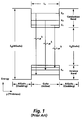
- Quantum levels are typically illustrated by a bound-state diagram such as that shown in Fig. 1 for a GaAs/Al x Ga 1-x As quantum well structure. See, e.g., Holonyak et al., Quantum-Well Heterostructure Lasers , IEEE J. Quant. Elec., vol. QE-16, no. 2, p. 170, (1980).
- the active layer having quantized states is essentially an energy "well" whose depth is a function of the bandgap of the active layer material and whose width is equal to the thickness of the active layer.
- Fig. 1 diagrams a single quantum well structure. However, by forming the active layer to have a number of bandgap changes, for example, multiple quantum wells may be formed.
- the motion of the individual carriers in the x and y directions is allowed over distances much larger than the de Broglie wavelength and therefore is not quantized.
- motion in one or both of the x and y directions may be restricted such that quantum size effects occur.
- Carriers e.g., electrons
- the total energy in the quantum well can not be less than E1 due to the energy quantization.
- E T the total energy
- This process of progressively filling unoccupied states of increasing energy is called "bandfilling" because the conduction band is filled with the increasing number of electrons and the valence band is filled with the increasing number of holes.
- Increasing the number of carriers further will eventually fill states with energy greater than E2 and thereby allow carriers to occupy states at the third quantum level E3 and so on. Similar bandfilling occurs with holes in the valence band.
- the wavelength of the light emitted in recombination is a function of the energy given up in recombination, as given by
- laser oscillation of wavelength ⁇ 1 corresponding to the recombination of carriers in quantum level E1 will occur in the resonator. If lasing in quantum level E1 is prevented while simultaneously increasing the injected current, the quantum well layer will bandfill, allowing carriers to occupy the second quantum level E2. When the injected current is increased sufficiently, laser oscillation of wavelength ⁇ 2 occurs.
- Additional disadvantages of various of the above-described methods and apparatus include: temperature cycling resulting from or required to vary the output wavelength accelerates the degradation of the performance of the laser, often to the point where the lifespan of the laser is significantly shortened; a number of the methods and apparatus are not adaptable to wavelength tuning during operation of the device (that is, once the diffraction grating is placed in the laser beam path it is not possible to practically and accurately adjust or change the grating or filter to alter the wavelength fed back to the laser); it is very difficult if not impossible to accurately heat only one laser of an array of lasers without affecting the neighboring lasers (this is also an issue when operating the laser in close proximity to other devices, such as transistors, when operating the laser in a small-scale integrated system); and, a number of the methods and apparatus require additional apparatus and control, for example to vary the laser's temperature.
- the present invention provides a coaxially emitting multiple wavelength solid state laser, comprising a plurality of contiguous layers of semiconductor material deposited on a substrate, one or more of said layers containing regions of carrier quantization in at least one dimension, wherein at least first and second regions thereof are formed such that one quantum level of said first region is at the same energy level as a different quantum level of said second region.
- the said regions of carrier quantization may comprise a multiple quantum well active region, the said first region being a first quantum well and the said second region being a second quantum well.
- the present invention accordingly also provides a coaxially emitting multiple wavelength solid state laser, comprising a plurality of contiguous layers of semiconductor material deposited on a substrate, one or more of said layers comprising a multiple quantum well active region of the type wherein at least two quantum wells contained therein are formed such that one quantum level of a first quantum well is at the same energy level as a different quantum level of a second quantum well.
- the present invention further provides a coaxially emitting multiple wavelength solid state laser, comprising a substrate; a first cladding layer disposed on said substrate; a multiple quantum well active layer disposed on said first cladding layer of the type having at least two adjacent quantum wells, a first of said quantum wells having a first energy bandgap between the lowest energy level of its conduction band and the uppermost level of its valence band a second of said quantum wells having a second energy bandgap between the lowest energy level of its conduction band and the uppermost level of its valence band which is less than the first energy bandgap, said first quantum well having at least one quantized state described by quantum number n and said second quantum well having at least two quantized states described by quantum number n and n', respectively, such that said quantized state n of said first well is at the same energy level as said quantized state n' of said second well, where n ⁇ n'; and a second cladding layer disposed on said multiple quantum well active layer.
- the said active layer may further include a third level quantum well having an energy bandgap between the lowest energy level of its conduction band and the uppermost level of its valence band equal to said first energy bandgap and further having at least one quantized state described by quantum number n'' such that said quantized state n'' of said third quantum well is at the same energy level as said quantized state n' of said second quantum well, where n' ⁇ n''.
- the present invention also provides a coaxially emitting multiple wavelength solid state laser, comprising a substrate; a first cladding layer disposed on said substrate; a multiple quantum well active layer disposed on said first cladding layer of the type having at least two adjacent quantum wells, a first of said quantum wells having a first thickness and a second of said quantum wells having a second thickness which is greater than the first thickness, said first quantum well having at least one quantized state described by quantum number n and second quantum well having at least two quantized states described by quantum numbers n and n', respectively, such that said quantized state n of said first well is at the same energy level as said quantized state n' of said second well, where n ⁇ n'; and a second cladding layer disposed on said multiple quantum well active layer.
- the said active layer may further include a third quantum well having a thickness equal to a first thickness and further having at least one quantized state described by quantum number n'' such that said quantized state n'' of said third quantum well is at the same energy level as said quantized state n' of said second quantum well, where n' ⁇ n''.
- a solid state semiconductor laser switchable between at least two different output wavelengths comprising a laser body of the type including a plurality of contiguous layers of semiconductor material, located in an optical path, said layers of the type providing regions of carrier quantization in at least one dimension, wherein at least first and second regions thereof are formed such that one quantum level of said first region is at the same energy level as a different quantum level of said second region; means for providing gain in said optical path when an electrical bias is applied thereto; means for providing loss in said optical path when an electrical bias is applied thereto to thereby limit the output of said laser to a first wavelength which corresponds to an energy level of said first region which is not found in said second region when a first electrical bias is applied thereto, and to thereby limit the output of said laser to a second wavelength different than said first wavelength which corresponds to an energy level found in both said first and second regions when a second electrical bias, different than said first electrical bias, is applied thereto.
- a solid state semiconductor laser switchable between at least two different output wavelengths comprising a laser body of the type including a plurality of contiguous layers of semiconductor material, located in an optical path, said layers of the type providing regions of carrier quantization in at least one dimension, wherein at least first and second regions thereof are formed such that one quantum level of said first region is at the same energy level as a different quantum level of said second region; means for providing gain in said optical path when an electrical bias is applied thereto; first loss means for providing loss in said optical path when an electrical bias is applied thereto to thereby limit the output of said laser to a first wavelength which corresponds to an energy level of said first region which is not found in said second region; second loss means for providing loss in said optical path when an electrical bias is applied thereto to thereby limit the output of said laser to a second wavelength different than said first wavelength which corresponds to an energy level found in both said first and second regions.
- the laser may further include means for switching an electrical bias such that said bias is applied either
- the first loss means comprises a waveguide of a first width
- said second loss means comprises a waveguide of a second width different than said first width.
- the first loss means comprises a waveguide of a first length
- said second loss means comprises a waveguide of a second length different than said first length.
- said means for providing gain and said first loss means are coupled by an optical waveguide, and said means for providing gain and said second loss means are not coupled by an optical waveguide.
- the present invention enables the provision of a multiple wavelength diode laser source having output intensity at both the shorter and longer wavelengths of operation more nearly equal than heretofore available.
- At the heart of embodiments of the present invention described herein is the structuring of the quantum wells of a multiple quantum well active layer so as to align the energy bands of different energy band number of at least two adjacent quantum wells.
- a diode laser source embodying this invention may comprise a MQW active layer disposed between upper and lower cladding layers. At least two quantum wells are formed in the active layer, a shallow well and a deep well. The shallow well is formed to have at least one energy band confined thereto, and the deep well is formed to have at least two energy bands confined thereto. The depth, thickness, and material composition of the shallow well and the deep well are selected such that the first energy band of the shallow well is at the same energy level as the second energy band of the deep well.
- the alignment may be between the first energy band of the shallow well and a third energy band of the deep well, the second energy band of the shallow well and the third energy band of the deep well, etc., again based on the depth, thickness, and material composition of the wells.
- the alignment of the energy bands allows the recombination of carriers from the deep well to augment the recombination of carriers from the shallow well. Since recombination in each energy band corresponds to a unique output wavelength, the alignment of the energy bands allows increased gain for the output wavelength corresponding to the aligned energy band (e.g., the wavelength corresponding to the first energy band of the shallow well).
- the number of wells, and the selected alignment of the quantum levels, determines the output intensity profile. Appropriate placement of the wells within the laser waveguide thus facilitates a matching of the output intensity profile with a desired output mode, e.g., the fundamental mode TE00. Uniform band filling is achieved by tunneling between wells or by simultaneous injection into all wells.
- the present invention may be embodied in two dimensionally quantized structures ("quantum wires") and three dimensionally quantized structures ("quantum dots”).
- the quantized regions may be designated by two or three quantum numbers, respectively, where at least one of the quantum numbers differs as between two regions with aligned energy bands.
- a basic quantum-well laser structure is fabricated, with certain modifications as detailed below.
- a basic quantum-well laser structure 10 which comprises an n-type GaAs substrate 12, upon which is epitaxially deposited an n-type Al x Ga 1-x As cladding layer 14, an Al y Ga 1-y As waveguide layer 16 where x>y, a GaAs quantum-well active layer 18 which is described in more detail below, an Al y Ga 1-y As waveguide layer 20, a p-type Al x Ga 1-x As cladding layer 22, and a p+-type cap layer 24.
- GaAs quantum-well active layer 18 is comprised of multiple alternating layers 26 and 28, respectively, of p, n, or undoped GaAs and Al z Ga 1-z As, with z ⁇ y. At the very least, there will be provided one layer each of layers 26 and 28, although as will be further discussed, the number, thickness and composition of each layer may be varied. The thickness of each of layers 26 and 28 will be on the order of the carrier de Broglie wavelength so that the layers exhibit the aforementioned quantum size effects (i.e., the carriers are quantized into different quantum levels) in one dimension.
- this structure is just one exemplary embodiment of the present invention, and that others, such as an array (not shown) of structures 10, a structure with quantum levels in two dimensions, or a so-called “quantum wire” (see, e.g., the above-mentioned European patent application No. 0494766), a structure with quantum levels in three dimensions, or a so-called “quantum dot” or “quantum box” (see, e.g., Asada et al., Gain and the Threshold of Three-Dimensional Quantum-Box Lasers , IEEE J. Quant. Elec., vol. QE-22, no. 9, p. 1915 (1986)), etc., formed by a wide variety of processes, such as MOCVD, LPE, impurity induced layer disordering ("IILD”), etc., may equally embody the present invention.
- MOCVD MOCVD
- LPE impurity induced layer disordering
- IILD impurity induced layer disordering
- electrons and holes confined to a quantum well can reside only in states with discrete energies in the direction normal to the quantum well layer. These quantized states or energy levels are denoted by integer quantum numbers. Light is produced when an electron in the nth energy level of the conduction band recombines with a hole in the mth energy level of the valence band of the same quantum well.
- E ⁇ E g + ⁇ E cn + ⁇ E vm (6)
- E g the intrinsic bandgap energy of the quantum well material
- ⁇ E cn the energy of the confined electron in the nth energy level relative to the conduction bandedge
- ⁇ E vm the energy of a confined hole in the mth energy level relative to the valence bandedge.
- ⁇ E cn is determined by the thickness of the quantum well and the energy difference V cb between the conduction bandedge of the quantum well and the conduction bandedge of adjacent widegap confining layers, e.g., Al y Ga 1-y As layers 16 and 20 (Fig. 2).
- the difference V cb is fixed by the relative compositions of the quantum well and its adjacent widegap material.
- ⁇ E vm is determined by the thickness of the quantum well and the energy difference V vb between the valence bandedge of the quantum well and the valence bandedge of adjacent widegap confining layers, e.g., Al y Ga 1-y As layers 16 and 20 (Fig. 2).
- the difference V vb is fixed by the relative compositions of the quantum well and its adjacent widegap material. From R.M. Kolbas and N. Holonyak, Jr., Man-made Quantum Wells: A New Perspective on the Finite Square-well Problem , Am. J. Phys., vol. 52, no. 5, p.
- the first equation determines the energy of the electronic state that is spatially symmetric in the quantum well
- the second equation determines the energy of the electronic state that is spatially antisymmetric in the quantum well.
- m h can have one of two values, 0.45m o (denoted the "heavy hole") or 0.082 m o (denoted the "light hole”).
- Recombination of an electron with the heavy hole is normally the transition that gives rise to lasing in a GaAs quantum well. Therefore, for purposes of the present explanation, only recombinations with heavy holes will be considered herein.
- recombination of electrons with holes is nearly forbidden if n ⁇ m.
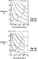
- Figs. 3a and 3b show the values of electron and hole energies for a GaAs layer sandwiched between two Al 0.35 Ga 0.65 As confining layers.
- ⁇ E c1 40 meV
- ⁇ E c2 148 meV
- ⁇ E v1 6 meV
- ⁇ E v2 22 meV.
- E g 1.424 eV for GaAs
- ⁇ (12398/1.47) ⁇ 843 nm.
- the nth level in the conduction band of one quantum well is aligned with the n'th (n>n') level in the conduction band of one or more other quantum wells in a MQW active layer.
- these two quantum wells are adjacent one another in the band diagram (i.e., are disposed directly above or below one another in the quantum well active layer), although they need not necessarily be so placed.
- Energy levels with different quantum numbers are aligned by properly choosing the thickness and/or composition of the quantum well layers.
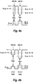
- Fig.4a To illustrate the procedure by which such a multiple wavelength active layer is designed, we consider a two well system composed of GaAs wells and Al 0.35 Ga 0.65 As confinement layers, as shown in Fig.4a.
- the thickness of the second quantum well is determined by step iii to be ⁇ 40 ⁇ .
- Alignment of the nth and n'th levels of two quantum wells in the conduction band such that each well has the same thickness is achieved by adjusting the composition of one well in order to increase its bandgap.
- a two well system composed of one GaAs well and one Al x Ga 1-x As well separated by a Al 0.35 Ga 0.65 As confinement layer, as shown in Fig. 4b. Both quantum wells have the same thickness, taken to be 100 ⁇ for illustration.
- Alignment of the nth level in one quantum well with the n'th level in another quantum well can also be achieved by simultaneously adjusting the thickness and composition of one well.
- the alignment of energy bands in two quantum wells within the same active layer is utilized to increase the gain at the output wavelength corresponding to the aligned energy bands and thereby decrease the threshold current required for lasing at that wavelength.
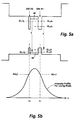
- Increased gain is achieved and controlled by proper positioning of the quantum wells relative to the intensity profile of the optical mode within the laser waveguide. The way in which this increased gain is achieved can be understood by referring to Figs. 5a through 5d.
- the gain of the mode, G( ⁇ 1), emitted at ⁇ 1 is proportional to A(x1)g1( ⁇ 1), where A(x1) is the relative intensity of the mode at x1 and g1( ⁇ 1) is the optical gain of the medium in quantum well 1 at ⁇ 1.
- the gain of the mode, G( ⁇ 2), emitted at ⁇ 2, is proportional to A(x1)g1( ⁇ 2) + A(x2)g2( ⁇ 2), where g1( ⁇ 2) is the optical gain in quantum well 1 at ⁇ 2, A(x2) is the relative intensity of the mode at x2, and g2( ⁇ 2) is the optical gain in quantum well 2 at ⁇ 2.
- G( ⁇ 2)/G( ⁇ 1) [g1( ⁇ 2)/g1( ⁇ 1)] + [A(x2)/A(x1)][g2( ⁇ 2)/g1( ⁇ 1)] (10)
- the first term on the right is the ratio of the material gain at ⁇ 2 to the material gain at ⁇ 1 for quantum well 1 and therefore gives the relative amount of gain for the two transitions without a second quantum well in the laser waveguide.
- the presence of the second well increases the gain at ⁇ 2 by [A(x2)/A(x1)][g2( ⁇ 2)/g1( ⁇ 1)].
- the threshold for the mode at ⁇ 2 will be less than its threshold with gain derived from only one quantum well.
- the wells can be spaced close enough to allow effective tunneling between (E c1 )2 and (E c2 )1.
- a structure for which the difference between thresholds at ⁇ 2 and ⁇ 1 is minimized can be achieved by placing quantum well 2 at the maximum of the intensity profile and choosing x1 -x2 to be greater than half the full width at half maximum for the lasing mode so that the ratio [A(x2)/A(x1)] is greater than 2. This is shown in Figs. 5c and 5d. Consequently, the gain of the mode at ⁇ 2 is enhanced relative to the gain obtained at ⁇ 1 for the same carrier density and the difference between their thresholds can be adjusted as desired by appropriately selecting x1. In this way the difference between the thresholds for lasing at ⁇ 2 and ⁇ 1 can be decreased to zero, thereby allowing the laser waveguide to lase simultaneously at two widely separated wavelengths if so desired.
- the quantum wells should be spaced by 0.5 ⁇ m or more. This distance is rather large for effectively injecting carriers into both wells from the cladding layers 14 and 22 shown in Fig. 2. However, carriers can be effectively coupled between wells with this separation by lowering the bandgap of the confining layer between them as shown by the dotted line 40 in Figs. 5a and 5c. For these structures, electrons injected from the n-side (right side of Figs. 5a and 5c) which fall into quantum well 1 will readily be thermalized into quantum well 2.
- a preferred structure for injecting an adequate number of carriers into both wells is a laterally injected laser waveguide such as that described by Thornton in United States patent serial no. 4,987,468, dated Jan. 22, 1991.
- An example of such a structure 50 is shown in Fig. 6.
- electrons are injected by n-type disordered regions 52 used to form the lateral extent of the waveguide while holes are supplied by the p-type quantum wells of region 54.
- Lasers defined in this way with uniform multiple quantum well active layers exhibit very low threshold as discussed in detail in the aforementioned patent.
- Figs. 7a and 7b illustrate the use of three quantum wells to reduce the threshold current for lasing at the shortest wavelength. Alignment of energy bands in three quantum wells within the same active layer provides an even greater increase in the gain at the output wavelength corresponding to the aligned energy bands than the embodiment comprising two quantum wells previously discussed. Alignment of the nth level in the conduction band of one quantum well with the n'th level in two adjacent wells, for example on either side of the first well (although they need not be so disposed), can be achieved by decreasing the thickness of the two adjacent wells as illustrated in Fig. 7a or by using three wells with the same thickness while adjusting the composition of the two adjacent wells to increase their bandgap as illustrated in Fig. 7b. The procedure for accomplishing these alignments is similar to that discussed previously and illustrated in Figs. 3a and 3b.
- Energy band alignment is used to decrease the threshold for the lasing mode at the shortest wavelength by proper positioning of the quantum wells relative to the intensity profile of the lasing mode within the laser waveguide.
- the advantage of the 3 well structure is readily seen by considering the relative gains of the modes emitted at ⁇ 1 and ⁇ 2.
- the thickest (or deepest) well, quantum well 1 in Fig. 8a is located at the position of maximum intensity of the lasing mode, as illustrated in Figs. 8a and 8b.
- the gain of the mode emitted at ⁇ 1, G( ⁇ 1) is proportional to A(x1)g1( ⁇ 1) and the gain of the mode emitted at ⁇ 2, G( ⁇ 2), is proportional to A(x1)g1( ⁇ 2) + A(x2)g2( ⁇ 2) + A(x3)g3( ⁇ 2), where A(x3) is the relative intensity of the mode at x3 and g3( ⁇ 2) is the optical gain of quantum well 3 at ⁇ 2.
- G( ⁇ 2)/G( ⁇ 1) [g1( ⁇ 2)/g1( ⁇ 1)] + [A(x2)/A(x1)][g2( ⁇ 2)/g1( ⁇ 1)] + [A(x3)/A(x1)][g3( ⁇ 2)/g1( ⁇ 1)] (11)
- the first term on the right is the ratio of the gain at ⁇ 2 to the gain at ⁇ 1 for a single quantum well and therefore gives the relative amounts of gain for the two transitions without other quantum wells in the laser waveguide.
- the presence of the second and third wells increases the gain at ⁇ 2 by [A(x2)/A(x1)][g2( ⁇ 2)/g1( ⁇ 1)] + [A(x3)/A(x1)][g3( ⁇ 2)/g1( ⁇ 1)].
- G( ⁇ 2) is maximized relative to G( ⁇ 1) by maximizing [A(x2)/A(x1)] and [A(x3)/A(x1)]. This is achieved by locating all the quantum wells near the position of maximum intensity of the lasing mode.
- a typical three well structure would include a central well of GaAs with thickness equal to 100 ⁇ spaced apart from two GaAs wells with thickness equal to 45 ⁇ by confinement layers of Al 0.35 Ga 0.65 As with thickness equal to 30 ⁇ . With 30 ⁇ confinement layers, tunneling will readily occur between (E c1 )2, (E c2 )1, and (E c1 )3 and help maintain a uniform distribution of carriers in all wells.
- Alignment of the nth level in one quantum well with the n'th level in two adjacent wells can also be achieved by simultaneously adjusting the thickness and composition of the two adjacent wells.
- a structure for which the difference between thresholds at ⁇ 2 and ⁇ 1 is minimized can be achieved by placing quantum wells 2 and 3 near the maximum of the intensity profile and choosing x1 - x2 and x1 - x3 greater than half the full width at half maximum for the lasing mode so that the ratios [A(x2)/A(x1)] and [A(x3)/A(x1)] are greater than 2. Consequently, the gain of the mode at ⁇ 2 is enhanced relative to the gain obtained at ⁇ 1 for the same carrier density and the difference between their thresholds can be adjusted as desired. Since the full width at half maximum for the optical mode in the laser waveguide is typically about 1 ⁇ m, quantum wells 2 and 3 should be spaced by 0.5 ⁇ m or more from quantum well 1.
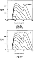
- Fig. 9a illustrates the modal gain G( ⁇ ) obtained at various levels of carrier density in a single quantum well. See for example, J. Z. Wilcox et al., Dependence of Emission Wavelength on Cavity Length and Facet Reflectivities in Multiple Quantum Well Semiconductor Lasers , Appl. Phys. Lett., vol. 54, no. 22, p. 2174, (1989).
- the gain spectrum is a single peaked function arising from recombination in quantum well 1 with emission at ⁇ 1.
- One method of selecting the wavelength of lasing emission is by controlling the loss in the laser cavity.
- One method of achieving this loss control is to introduce a small but separately contacted modulator region along the axis of the laser as well known in the art. See for example, Thornton et al., U.S. patent serial no. 4,802,182.
- An example of such a structure 100 is shown in Fig. 10, where a narrow optical waveguide 102 is used to optically couple and simultaneously electrically isolate an amplifier region 104 and a modulator region 106 of the laser cavity.
- Structure 100 can be fabricated, for example, by IILD as described by Thornton et al. in U.S. patent serial no. 4,802,182, or by other techniques known to those skilled in the art.
- Wavelength switching within the laser waveguide of laser 100 is achieved by controlling the optical loss introduced by modulator region 106.
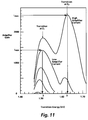
- the lasing photon wavelength is established where the gain of amplifier region 104 equals the loss of the laser cavity, including absorption in modulator region 106, as illustrated in Fig. 11.
- the total loss present in the laser cavity is varied by changing the bias level on modulator region 106 from a maximum value L max obtained when modulator region 106 is reverse biased or unbiased to a minimum value L min obtained with an appropriate level of current applied to modulator region 106.
- the enhanced gain in a laser according to this invention enables this condition to be achieved at a current lower than that obtained with SQW or MQW active layers in lasers not formed according to this invention.
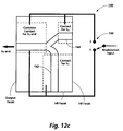
- Figs. 12a, 12b, and 12c Alternate embodiments for switching the wavelength of lasing emission from MQW structures in lasers formed according to this invention are shown in Figs. 12a, 12b, and 12c.
- Fig. 12a shows a laser 120 whose cavity is bifurcated into two laterally separated waveguides 122 and 124 with different optical loss. Different levels of optical loss can be achieved from each waveguide, for example, by narrowing the width of one active waveguide 126 relative to the other active waveguide 128.
- each waveguide 132 and 134 of a laser apparatus 130 can be achieved by appropriate design of the coupling region, as illustrated in Fig. 12b.
- region 134 is optically coupled to a gain region 105 by a waveguide region 107, while region 132 is only evanescently coupled to gain region 105.
- the increased loss introduced by the evanescent coupling between the offset laser waveguides 132 and 134 causes lasing on the offset path from waveguide 132 to occur at the short wavelength ⁇ 2.
- two waveguides 142 and 144 of a laser apparatus 140 can be made with different lengths as shown in Fig. 12c. Because the longer waveguide 142 has more total gain than the shorter waveguide 144 it will lase on the long wavelength transition ⁇ 1.
- Lasing at ⁇ 1 is obtained in each of the embodiments of Figs. 12a, 12b, and 12c by applying current to the structure with the switch 150 of the various embodiments in position 1. In this position, no current is applied to the contact for ⁇ 2 and consequently no lasing occurs in this region since it is highly absorptive.
- the lasing wavelength is switched from ⁇ 1 to ⁇ 2 by applying increased current through the switch in position 2. In this position, no current is applied to the contact for ⁇ 1, and consequently lasing at ⁇ 1 is suppressed since this region is highly absorptive.
- Coaxial emission of light at ⁇ 1 and ⁇ 2 is obtained from the indicated output facet since this portion of the laser cavity is common to the optical path of each waveguide.
- the present invention may be embodied in structures having regions of carrier quantization in two dimensions ("quantum wires").
- the regions of quantization may be designated by two quantum numbers, for example x and y, where at least one of the quantum numbers differs as between two regions with aligned energy bands. This is shown in Fig. 13.
- the present invention may be embodied in structures having regions of carrier quantization in three dimensions ("quantum wires") such as those structures disclosed by Stern et al., in Fabrication of 20-nm Structures in GaAs , Appl. Phys. Lett., vol. 45, no. 4, p.
- the regions of carrier quantization may be designated by three quantum numbers, again, at least one of the quantum numbers must be different as between two regions with aligned energy bands.
- the double quantum wire structure of Simhony et al. disclosed in Double Quantum Wire GaAs/AlGaAs Diode Lasers Grown By Organometallic Chemical Vapor Deposition On Grooved Substrates , IEEE Phot. Tech. Lett., vol. 2, no. 5, p.305 (1990), may be configured to have energy band alignment as required for a laser according to the present invention.
- regions of carrier quantization may lie in different planes of the device.
- the stacked quantum wires disclosed in the above-mentioned European patent No. 0494766 may also be configured to have energy band alignment according to the present invention.
Landscapes
- Physics & Mathematics (AREA)
- Electromagnetism (AREA)
- Optics & Photonics (AREA)
- Engineering & Computer Science (AREA)
- Nanotechnology (AREA)
- Chemical & Material Sciences (AREA)
- Crystallography & Structural Chemistry (AREA)
- Biophysics (AREA)
- Life Sciences & Earth Sciences (AREA)
- Plasma & Fusion (AREA)
- Condensed Matter Physics & Semiconductors (AREA)
- General Physics & Mathematics (AREA)
- Semiconductor Lasers (AREA)
Applications Claiming Priority (4)
| Application Number | Priority Date | Filing Date | Title |
|---|---|---|---|
| US779207 | 1991-10-18 | ||
| US07/779,207 US5214664A (en) | 1991-10-18 | 1991-10-18 | Multiple wavelength semiconductor laser |
| US07/779,211 US5200969A (en) | 1991-10-18 | 1991-10-18 | Switchable multiple wavelength semiconductor laser |
| US779211 | 1991-10-18 |
Publications (2)
| Publication Number | Publication Date |
|---|---|
| EP0539015A1 true EP0539015A1 (fr) | 1993-04-28 |
| EP0539015B1 EP0539015B1 (fr) | 1996-10-16 |
Family
ID=27119550
Family Applications (1)
| Application Number | Title | Priority Date | Filing Date |
|---|---|---|---|
| EP19920308463 Expired - Lifetime EP0539015B1 (fr) | 1991-10-18 | 1992-09-17 | Laser à semi-conducteur à longueurs d'ondes multiples |
Country Status (2)
| Country | Link |
|---|---|
| EP (1) | EP0539015B1 (fr) |
| DE (1) | DE69214595T2 (fr) |
Cited By (1)
| Publication number | Priority date | Publication date | Assignee | Title |
|---|---|---|---|---|
| WO1998010544A3 (fr) * | 1996-09-04 | 2000-11-09 | Ericsson Telefon Ab L M | Production de lumiere de longueurs d'onde differentes au moyen d'un laser |
Citations (5)
| Publication number | Priority date | Publication date | Assignee | Title |
|---|---|---|---|---|
| EP0254568A2 (fr) * | 1986-07-25 | 1988-01-27 | Mitsubishi Denki Kabushiki Kaisha | Dispositif laser à semi-conducteur |
| US4802182A (en) * | 1987-11-05 | 1989-01-31 | Xerox Corporation | Monolithic two dimensional waveguide coupled cavity laser/modulator |
| EP0361399A2 (fr) * | 1988-09-28 | 1990-04-04 | Canon Kabushiki Kaisha | Réseau laser à semi-conducteur contenant des lasers avec des moyens de reflexion présentant des propriétés de sélection de longueur d'onde différentes |
| EP0390167A2 (fr) * | 1989-03-30 | 1990-10-03 | Canon Kabushiki Kaisha | Laser à semi-conducteur muni de couches multiples pour l'émission de lumière de longueurs d'ondes différentes et méthode de commande |
| EP0444709A2 (fr) * | 1990-03-02 | 1991-09-04 | Canon Kabushiki Kaisha | Laser à semi-conducteur avec pluralité de couches émettant à différentes longueurs d'ondes et sa méthode de commande |
-
1992
- 1992-09-17 EP EP19920308463 patent/EP0539015B1/fr not_active Expired - Lifetime
- 1992-09-17 DE DE1992614595 patent/DE69214595T2/de not_active Expired - Fee Related
Patent Citations (5)
| Publication number | Priority date | Publication date | Assignee | Title |
|---|---|---|---|---|
| EP0254568A2 (fr) * | 1986-07-25 | 1988-01-27 | Mitsubishi Denki Kabushiki Kaisha | Dispositif laser à semi-conducteur |
| US4802182A (en) * | 1987-11-05 | 1989-01-31 | Xerox Corporation | Monolithic two dimensional waveguide coupled cavity laser/modulator |
| EP0361399A2 (fr) * | 1988-09-28 | 1990-04-04 | Canon Kabushiki Kaisha | Réseau laser à semi-conducteur contenant des lasers avec des moyens de reflexion présentant des propriétés de sélection de longueur d'onde différentes |
| EP0390167A2 (fr) * | 1989-03-30 | 1990-10-03 | Canon Kabushiki Kaisha | Laser à semi-conducteur muni de couches multiples pour l'émission de lumière de longueurs d'ondes différentes et méthode de commande |
| EP0444709A2 (fr) * | 1990-03-02 | 1991-09-04 | Canon Kabushiki Kaisha | Laser à semi-conducteur avec pluralité de couches émettant à différentes longueurs d'ondes et sa méthode de commande |
Cited By (2)
| Publication number | Priority date | Publication date | Assignee | Title |
|---|---|---|---|---|
| WO1998010544A3 (fr) * | 1996-09-04 | 2000-11-09 | Ericsson Telefon Ab L M | Production de lumiere de longueurs d'onde differentes au moyen d'un laser |
| KR100411871B1 (ko) * | 1996-09-04 | 2003-12-24 | 텔레폰악티에볼라겟엘엠에릭슨(펍) | 발광 장치 |
Also Published As
| Publication number | Publication date |
|---|---|
| DE69214595T2 (de) | 1997-03-13 |
| DE69214595D1 (de) | 1996-11-21 |
| EP0539015B1 (fr) | 1996-10-16 |
Similar Documents
| Publication | Publication Date | Title |
|---|---|---|
| US5214664A (en) | Multiple wavelength semiconductor laser | |
| US5200969A (en) | Switchable multiple wavelength semiconductor laser | |
| EP0547043B1 (fr) | Dispositif laser à semi-conducteur | |
| Botez et al. | Phase-locked arrays of semiconductor diode lasers | |
| JP3251386B2 (ja) | 偏光切換可能量子井戸レーザ | |
| JP3536987B2 (ja) | 多ビーム半導体量子井戸レーザ | |
| US7075954B2 (en) | Intelligent wavelength division multiplexing systems based on arrays of wavelength tunable lasers and wavelength tunable resonant photodetectors | |
| EP0206496A2 (fr) | Réseau laser semi-conducteur à commande de phase | |
| JP2007116200A (ja) | 量子ダッシュデバイス | |
| Mukai et al. | Fundamental mode oscillation of a buried ridge waveguide laser array | |
| US20030007531A1 (en) | Polarization controlled VCSELs using an asymmetric current confining aperture | |
| US7573926B2 (en) | Multiwavelength quantum dot laser element | |
| US4982408A (en) | Variable oscillation wavelength semiconduction laser device | |
| US5675605A (en) | Semiconductor surface-emitting optical device having light emitting layer of ordered crystal structure sandwiched between bragg reflectors | |
| JP2004253802A (ja) | 改善された温度特性を有するGaAsSb/GaAs素子 | |
| US6560265B2 (en) | Method and apparatus for polarizing light in a VCSEL | |
| EP0539015B1 (fr) | Laser à semi-conducteur à longueurs d'ondes multiples | |
| JPH05211346A (ja) | 面形発光素子 | |
| US5670789A (en) | Semiconductor light-emitting device with quantum well structure | |
| JPS6332982A (ja) | 半導体レ−ザ | |
| Zmudzinski et al. | 1 W diffraction-limited-beam operation of resonant-optical-waveguide diode laser arrays at 0.98 μm | |
| Figueroa et al. | Modeling of the optical characteristics for twin-channel laser (TCL) structures | |
| US5309472A (en) | Semiconductor device and a method for producing the same | |
| JP4957355B2 (ja) | 半導体発光素子 | |
| Pospiech et al. | Laser diodes |
Legal Events
| Date | Code | Title | Description |
|---|---|---|---|
| PUAI | Public reference made under article 153(3) epc to a published international application that has entered the european phase |
Free format text: ORIGINAL CODE: 0009012 |
|
| AK | Designated contracting states |
Kind code of ref document: A1 Designated state(s): DE FR GB NL |
|
| 17P | Request for examination filed |
Effective date: 19931005 |
|
| 17Q | First examination report despatched |
Effective date: 19940926 |
|
| GRAG | Despatch of communication of intention to grant |
Free format text: ORIGINAL CODE: EPIDOS AGRA |
|
| GRAH | Despatch of communication of intention to grant a patent |
Free format text: ORIGINAL CODE: EPIDOS IGRA |
|
| GRAH | Despatch of communication of intention to grant a patent |
Free format text: ORIGINAL CODE: EPIDOS IGRA |
|
| GRAA | (expected) grant |
Free format text: ORIGINAL CODE: 0009210 |
|
| AK | Designated contracting states |
Kind code of ref document: B1 Designated state(s): DE FR GB NL |
|
| REF | Corresponds to: |
Ref document number: 69214595 Country of ref document: DE Date of ref document: 19961121 |
|
| ET | Fr: translation filed | ||
| PLBE | No opposition filed within time limit |
Free format text: ORIGINAL CODE: 0009261 |
|
| 26N | No opposition filed | ||
| REG | Reference to a national code |
Ref country code: GB Ref legal event code: IF02 |
|
| PGFP | Annual fee paid to national office [announced via postgrant information from national office to epo] |
Ref country code: FR Payment date: 20050823 Year of fee payment: 14 |
|
| PGFP | Annual fee paid to national office [announced via postgrant information from national office to epo] |
Ref country code: NL Payment date: 20050904 Year of fee payment: 14 |
|
| PGFP | Annual fee paid to national office [announced via postgrant information from national office to epo] |
Ref country code: GB Payment date: 20050914 Year of fee payment: 14 |
|
| PGFP | Annual fee paid to national office [announced via postgrant information from national office to epo] |
Ref country code: DE Payment date: 20050915 Year of fee payment: 14 |
|
| PG25 | Lapsed in a contracting state [announced via postgrant information from national office to epo] |
Ref country code: NL Free format text: LAPSE BECAUSE OF NON-PAYMENT OF DUE FEES Effective date: 20070401 |
|
| PG25 | Lapsed in a contracting state [announced via postgrant information from national office to epo] |
Ref country code: DE Free format text: LAPSE BECAUSE OF NON-PAYMENT OF DUE FEES Effective date: 20070403 |
|
| GBPC | Gb: european patent ceased through non-payment of renewal fee |
Effective date: 20060917 |
|
| NLV4 | Nl: lapsed or anulled due to non-payment of the annual fee |
Effective date: 20070401 |
|
| REG | Reference to a national code |
Ref country code: FR Ref legal event code: ST Effective date: 20070531 |
|
| PG25 | Lapsed in a contracting state [announced via postgrant information from national office to epo] |
Ref country code: GB Free format text: LAPSE BECAUSE OF NON-PAYMENT OF DUE FEES Effective date: 20060917 |
|
| PG25 | Lapsed in a contracting state [announced via postgrant information from national office to epo] |
Ref country code: FR Free format text: LAPSE BECAUSE OF NON-PAYMENT OF DUE FEES Effective date: 20061002 |