EP0540176A1 - Sous-système électronique expansible pour imprimeur - Google Patents
Sous-système électronique expansible pour imprimeur Download PDFInfo
- Publication number
- EP0540176A1 EP0540176A1 EP92308882A EP92308882A EP0540176A1 EP 0540176 A1 EP0540176 A1 EP 0540176A1 EP 92308882 A EP92308882 A EP 92308882A EP 92308882 A EP92308882 A EP 92308882A EP 0540176 A1 EP0540176 A1 EP 0540176A1
- Authority
- EP
- European Patent Office
- Prior art keywords
- data
- discrete input
- module
- bus
- output module
- Prior art date
- Legal status (The legal status is an assumption and is not a legal conclusion. Google has not performed a legal analysis and makes no representation as to the accuracy of the status listed.)
- Withdrawn
Links
Images








Classifications
-
- H—ELECTRICITY
- H04—ELECTRIC COMMUNICATION TECHNIQUE
- H04N—PICTORIAL COMMUNICATION, e.g. TELEVISION
- H04N1/00—Scanning, transmission or reproduction of documents or the like, e.g. facsimile transmission; Details thereof
- H04N1/32—Circuits or arrangements for control or supervision between transmitter and receiver or between image input and image output device, e.g. between a still-image camera and its memory or between a still-image camera and a printer device
- H04N1/32502—Circuits or arrangements for control or supervision between transmitter and receiver or between image input and image output device, e.g. between a still-image camera and its memory or between a still-image camera and a printer device in systems having a plurality of input or output devices
- H04N1/32507—Circuits or arrangements for control or supervision between transmitter and receiver or between image input and image output device, e.g. between a still-image camera and its memory or between a still-image camera and a printer device in systems having a plurality of input or output devices a plurality of input devices
- H04N1/32512—Circuits or arrangements for control or supervision between transmitter and receiver or between image input and image output device, e.g. between a still-image camera and its memory or between a still-image camera and a printer device in systems having a plurality of input or output devices a plurality of input devices of different type, e.g. internal and external devices
-
- G—PHYSICS
- G06—COMPUTING OR CALCULATING; COUNTING
- G06K—GRAPHICAL DATA READING; PRESENTATION OF DATA; RECORD CARRIERS; HANDLING RECORD CARRIERS
- G06K15/00—Arrangements for producing a permanent visual presentation of the output data, e.g. computer output printers
-
- H—ELECTRICITY
- H04—ELECTRIC COMMUNICATION TECHNIQUE
- H04N—PICTORIAL COMMUNICATION, e.g. TELEVISION
- H04N1/00—Scanning, transmission or reproduction of documents or the like, e.g. facsimile transmission; Details thereof
- H04N1/00912—Arrangements for controlling a still picture apparatus or components thereof not otherwise provided for
- H04N1/0096—Simultaneous or quasi-simultaneous functioning of a plurality of operations
-
- H—ELECTRICITY
- H04—ELECTRIC COMMUNICATION TECHNIQUE
- H04N—PICTORIAL COMMUNICATION, e.g. TELEVISION
- H04N1/00—Scanning, transmission or reproduction of documents or the like, e.g. facsimile transmission; Details thereof
- H04N1/32—Circuits or arrangements for control or supervision between transmitter and receiver or between image input and image output device, e.g. between a still-image camera and its memory or between a still-image camera and a printer device
- H04N1/32502—Circuits or arrangements for control or supervision between transmitter and receiver or between image input and image output device, e.g. between a still-image camera and its memory or between a still-image camera and a printer device in systems having a plurality of input or output devices
- H04N1/32523—Circuits or arrangements for control or supervision between transmitter and receiver or between image input and image output device, e.g. between a still-image camera and its memory or between a still-image camera and a printer device in systems having a plurality of input or output devices a plurality of output devices
- H04N1/32529—Circuits or arrangements for control or supervision between transmitter and receiver or between image input and image output device, e.g. between a still-image camera and its memory or between a still-image camera and a printer device in systems having a plurality of input or output devices a plurality of output devices of different type, e.g. internal and external devices
-
- H—ELECTRICITY
- H04—ELECTRIC COMMUNICATION TECHNIQUE
- H04N—PICTORIAL COMMUNICATION, e.g. TELEVISION
- H04N1/00—Scanning, transmission or reproduction of documents or the like, e.g. facsimile transmission; Details thereof
- H04N1/32—Circuits or arrangements for control or supervision between transmitter and receiver or between image input and image output device, e.g. between a still-image camera and its memory or between a still-image camera and a printer device
- H04N1/32561—Circuits or arrangements for control or supervision between transmitter and receiver or between image input and image output device, e.g. between a still-image camera and its memory or between a still-image camera and a printer device using a programmed control device, e.g. a microprocessor
-
- H—ELECTRICITY
- H04—ELECTRIC COMMUNICATION TECHNIQUE
- H04N—PICTORIAL COMMUNICATION, e.g. TELEVISION
- H04N1/00—Scanning, transmission or reproduction of documents or the like, e.g. facsimile transmission; Details thereof
- H04N1/32—Circuits or arrangements for control or supervision between transmitter and receiver or between image input and image output device, e.g. between a still-image camera and its memory or between a still-image camera and a printer device
- H04N1/32561—Circuits or arrangements for control or supervision between transmitter and receiver or between image input and image output device, e.g. between a still-image camera and its memory or between a still-image camera and a printer device using a programmed control device, e.g. a microprocessor
- H04N1/32598—Bus based systems
- H04N1/32603—Multi-bus systems
-
- H—ELECTRICITY
- H04—ELECTRIC COMMUNICATION TECHNIQUE
- H04N—PICTORIAL COMMUNICATION, e.g. TELEVISION
- H04N1/00—Scanning, transmission or reproduction of documents or the like, e.g. facsimile transmission; Details thereof
- H04N1/00127—Connection or combination of a still picture apparatus with another apparatus, e.g. for storage, processing or transmission of still picture signals or of information associated with a still picture
- H04N1/00204—Connection or combination of a still picture apparatus with another apparatus, e.g. for storage, processing or transmission of still picture signals or of information associated with a still picture with a digital computer or a digital computer system, e.g. an internet server
-
- H—ELECTRICITY
- H04—ELECTRIC COMMUNICATION TECHNIQUE
- H04N—PICTORIAL COMMUNICATION, e.g. TELEVISION
- H04N2201/00—Indexing scheme relating to scanning, transmission or reproduction of documents or the like, and to details thereof
- H04N2201/0077—Types of the still picture apparatus
- H04N2201/0081—Image reader
-
- H—ELECTRICITY
- H04—ELECTRIC COMMUNICATION TECHNIQUE
- H04N—PICTORIAL COMMUNICATION, e.g. TELEVISION
- H04N2201/00—Indexing scheme relating to scanning, transmission or reproduction of documents or the like, and to details thereof
- H04N2201/0077—Types of the still picture apparatus
- H04N2201/0082—Image hardcopy reproducer
-
- H—ELECTRICITY
- H04—ELECTRIC COMMUNICATION TECHNIQUE
- H04N—PICTORIAL COMMUNICATION, e.g. TELEVISION
- H04N2201/00—Indexing scheme relating to scanning, transmission or reproduction of documents or the like, and to details thereof
- H04N2201/0077—Types of the still picture apparatus
- H04N2201/0086—Image transceiver
-
- H—ELECTRICITY
- H04—ELECTRIC COMMUNICATION TECHNIQUE
- H04N—PICTORIAL COMMUNICATION, e.g. TELEVISION
- H04N2201/00—Indexing scheme relating to scanning, transmission or reproduction of documents or the like, and to details thereof
- H04N2201/0077—Types of the still picture apparatus
- H04N2201/0089—Image display device
-
- H—ELECTRICITY
- H04—ELECTRIC COMMUNICATION TECHNIQUE
- H04N—PICTORIAL COMMUNICATION, e.g. TELEVISION
- H04N2201/00—Indexing scheme relating to scanning, transmission or reproduction of documents or the like, and to details thereof
- H04N2201/32—Circuits or arrangements for control or supervision between transmitter and receiver or between image input and image output device, e.g. between a still-image camera and its memory or between a still-image camera and a printer device
- H04N2201/3285—Circuits or arrangements for control or supervision between transmitter and receiver or between image input and image output device, e.g. between a still-image camera and its memory or between a still-image camera and a printer device using picture signal storage, e.g. at transmitter
- H04N2201/3287—Storage of at least one complete document page or image frame
-
- H—ELECTRICITY
- H04—ELECTRIC COMMUNICATION TECHNIQUE
- H04N—PICTORIAL COMMUNICATION, e.g. TELEVISION
- H04N2201/00—Indexing scheme relating to scanning, transmission or reproduction of documents or the like, and to details thereof
- H04N2201/32—Circuits or arrangements for control or supervision between transmitter and receiver or between image input and image output device, e.g. between a still-image camera and its memory or between a still-image camera and a printer device
- H04N2201/3285—Circuits or arrangements for control or supervision between transmitter and receiver or between image input and image output device, e.g. between a still-image camera and its memory or between a still-image camera and a printer device using picture signal storage, e.g. at transmitter
- H04N2201/3288—Storage of two or more complete document pages or image frames
Definitions
- the present invention relates generally to a printing apparatus, and more particularly to an improved expandable modular-based electronic subsystem capable of performing a plurality of operations substantially concurrently.
- the NP-9030 was one of the first electronic reprographic systems to be marketed with the capability to convert an optical image from a scanned original to image intensity signals, and reconstruct the signals, by way of a print engine using a pulsed diode laser. Because of the many image processing capabilities of the electronic reprographic system, which allows for, among other things, cut and paste operations, these types of systems are gaining enormous in popularity. While the NP-9030 was, when first introduced, a revolutionary product, it can no longer keep pace with advancements in the art, many of which are spurred on by advancements in related art areas, such as facsimile and computer.
- a relatively inexpensive electronic reprographic machine is disclosed in RESEARCH DISCLOSURE, No. 32388, March, 1991.
- This machine comprises a scanner communicating with a memory section and a Video Processor (VP) by way of a CPU.
- VP Video Processor
- image data can be transmitted to addresses configured in the memory by the CPU.
- the image data can be retrieved from memory and processed with the VP.
- a printing machine of the type in which image data, addresses and control data can be substantially concurrently transferred across multiple multipurpose buses, comprises a first multipurpose bus adapted to substantially concurrently transfer a first set of the image data, addresses and control data; a second multipurpose bus adapted to substantially concurrently transfer a second set of the image data, addresses and control data; a module for processing the first and second sets of data, which communicates with the first and second multipurpose buses; a first discreted
- Both the first processing module and the first discrete input/output module are adapted to transfer the first set of data between one another.
- the second and third discrete input/output modules are adapted to transfer the second set of data between one another.
- the first set of data can be transferred between the processing module and the first discrete input/output module substantially concurrent with the second set of data being transferred between the second discrete input/output module and the third discrete input/output module.
- a selected one of the discrete input/output modules may comprise means for scanning an original document, said scanning means being controlled by said processing module.
- the printing machine may further comprise a raster output scanning device, said raster output scanning device being controlled by said processing module.
- the said processing module may comprise a microprocessor.
- a printing machine in accordance with the present invention may also comprise a charge retentive member; means for charging said charge retentive member, said raster output scanning device being adapted to selectively discharge a surface of said charge retentive member to form an intelligible pattern of charged and discharged areas on said charge retentive member; means for developing the intelligible pattern on said charge retentive member to form a developed pattern thereon; and means for transferring the developed pattern from said charge retentive member to a substrate.
- the printing machine may further comprise a third multipurpose bus adapted to substantially concurrently transfer a third set of the image data, addresses and control data; a second processing module for processing the third set of data, which communicates with the third multipurpose bus; and a fourth discrete input/ output module which communicates with the third multipurpose bus.
- Both of the second processing modules and the fourth discrete input/output module are adapted to transfer the third set of data between one another.
- the third set of data can be transferred between the second processing module and the fourth discrete input/output module substantially concurrent with both the first set of data being transferred between the first processing module and the first input/output module and the second set of data being transferred between the second discrete input/output module and the third discrete input/output module.
- the fourth discrete input/output module may communicate with said first multipurpose bus so that said fourth discrete input/output module can communicate with a selected one of said first discrete input/output module and said first processing module.
- the fourth discrete input/output module may communicate with said second multipurpose bus so that said fourth discrete input/output module can communicate with a selected one of said second and third discrete input/output modules.
- said first discrete input/output module communicates with said second multipurpose bus, then said first, second and third sets of data can be transferred across said second multipurpose bus between any two of said first, second, third and fourth discrete input/output modules.
- said second processing module comprises a direct memory access device and a memory section; and said direct memory access device is capable of enabling data transfer between said memory section and said fourth discrete input-output.
- the memory section may comprise a disk drive device.
- said second processing module comprises a direct memory access device and a local area network module; and said direct memory access device is capable of enabling data transfer between said local area network module and said fourth discrete input/output module.
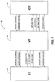
- the printing apparatus 10 for processing image data.
- the printing apparatus 10 comprises an image input terminal (IIT) 12, image output terminal (IOT) 14, and a video processor (VP) 16.
- IIT image input terminal
- IOT image output terminal
- VP video processor
- the IIT 12, the IOT 14 and the VP 16 are shown in a digital copying apparatus.
- the concepts underlying the printing apparatus 10 are applicable to many types of machines employing a scanning device coupled with a printing or output device.
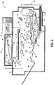
- the IIT 12 ( Figure 2) includes a scanning section having an automatic document handler (ADH) 20 for automatically and sequentially placing one or more documents 21 on a transparent platen 22.
- ADH automatic document handler
- the document 21 to be scanned is brought from a document tray 24 forward by the document handlers 26,27 into position on the platen 22 for scanning. Following scanning, the document 21 is returned to the document tray 24. While a particular document handler is shown, one skilled in the art will appreciate that other document handler types may be used instead or the documents 21 may be placed manually on the platen 22
- the scanning section of the IIT 12 employs one or more linear scanning arrays 30, which arrays 30 may comprise charge couple devices (CCDs) supported below and in scanning relation to the platen by a carriage 32.
- CCDs charge couple devices
- the carriage 32 can be reciprocated by reciprocating means 34, the reciprocating means 34 being similar to the reciprocating arrangement disclosed in US-A-4,387,636 to Daniele et al.
- a suitable lens 36 is provided to focus arrays 30 on a line-like segment of the platen 22 and the documents resting thereon.
- a suitable lamp 38 illuminates the document line being scanned.
- arrays 30 provide electrical image data or pixels representative of the document image scanned which are inputted to the VP 16 across a suitable IIT interface 42.
- the image data may be used for purposes other than printing copies, as for example, the image data may be transmitted via a communication channel (not shown) to another location, or stored, etc.
- the interface 42 includes differential transmitters/receivers and appropriate control logic adapted to provide data/control flow between the IIT 12 and the VP 16.
- interface 42 provides for an 8 bit wide image data bus 44 having a constant transfer rate of 4 Mbytes/sec.
- Image data is transmitted from the VP 16--the structure and operation of which VP 16 is explained in further detail below--to the IOT 14 by way of an IOT interface 46.
- the IOT 46 provides image data and control signal paths between the IOT 14 and the VP 16, and also includes two two scan line deep ping-pong buffers (not shown), the ping-pong buffers preferably being two 2K x 8 SRAMs.
- the image data is clocked out of the IOT interface 46 by way of a byte clock (not shown).
- the IOT 14 includes a raster output scanner (ROS) 50 having a suitable source of high intensity light, such as laser 52, modulated in accordance with the content of the image data as by an acousto-optic modulator 54 to provide zero and first order imaging beams.
- the imaging beam is scanned across a photoreceptor 56 at an exposing station 58 by a scanning polygon 60 to expose the previously charged photoreceptor 56 and create a latent electrostatic image or the document represented by the image signals to modulator 54.
- Suitable means (not shown) are employed to focus the beam on the photoreceptor 56.
- the printing apparatus 10 illustrated in Figure 2 employs a removable processing cartridge 64 which may be inserted and withdrawn from the main machine frame in the direction of arrow 66.
- Cartridge 64 includes the photoreceptor 56, which in one example comprises a belt like member 68, the outer periphery of the belt like member 68 being coated with a suitable photoconductive material 70.
- the belt 68 is suitably mounted for revolution within the cartridge 64 about driven transport roll 72, around idler roll 74 and travels in the direction indicated by the arrows on the inner run of the belt to bring the image bearing surface thereon past the plurality of xerographic processing stations.
- Suitable drive means such as a motor, not shown, are provided to power and coordinate the motion of the various cooperating machine components whereby a faithful reproduction of the original input scene information is recorded upon a sheet of final support material 76, such as paper or the like.
- the belt 68 moves the photoconductive surface 70 through a charging station 78 wherein the belt 68 is uniformly charged with an electrostatic charge placed on the photoconductive surface 70 by charge corotron 80 in known manner preparatory to imaging. Thereafter, the belt 68 is driven to the exposure station 58 wherein the charged photoconductive surface 70 is exposed to line-by-line scanning of the ROS 50, whereby the charge is selectively dissipated in the light exposed regions to record the original input image in the form of electrostatic latent image.
- the speed of the scanning carriage 32 and the speed of the belt 68 are synchronized to provide faithful reproduction of the original document.
- the development station 82 includes a magnetic brush development system including developer roll 86 utilizing a magnetizable developer mix having course magnetic carrier granules and toner colorant particles.
- Sheets 76 of the final support material are supported in a stack arranged on elevated stack support tray 88. With the stack at its elevated position, the sheet separator segmented feed roll 90 feeds individual sheets therefrom to the registration pinch roll pair 92. The sheet 76 is then forwarded to a transfer station 94 in proper registration with the image on the belt and the developed image on the photoconductive surface 70 is brought into contact with the sheet 76 of final support material within the transfer station 94 and the toner image is transferred from the photoconductive surface 70 to the contacting side of the final support sheet 76 by means of transfer corotron 96.
- the final support material 76 is separated from the belt 68 by the beam strength of the support material 76 as it passes around the idler roll 74, and the sheet 76 containing the toner image thereon is advanced to fixing station 98 wherein roll fuser 100 fixes the transferred powder image thereto. After fusing the toner image to the sheet 76, it is advanced by output rolls 102 to sheet stacking tray 104.
- toner particles remaining on the photoconductive surface after the transfer operation are removed from the belt 70 by a cleaning station 108, which cleaning station 108 comprises a cleaning blade 110 in scrapping contact with the outer periphery of the belt 68 and contained within a cleaning housing 112, the cleaning housing 112 having a cleaning seal 114 associated with the upstream opening of the cleaning housing 112.
- the toner particles may be mechanically cleaned from the photoconductive surface by a cleaning brush as is well known in the art.
- the VP 16 comprises an input network 116, a first memory interface network 118, a memory network 120, a computer network 122 and a second memory interface network 124.
- the input network 116 comprises a multiplexor (MUX) 126 as well as a user interface (UI) 130 coupled with suitable UI logic circuitry 132.
- MUX multiplexor
- UI user interface
- a 16-bit bus 134 allows the MUX 126 and the UI logic circuitry 132 to communicate with the computer network 122.
- the 8-bit image data bus 44 communicates with the MUX 126 and the UI logic circuitry 132.
- the UI 130 includes conventional control circuitry coupled with a CRT, the control circuitry being adapted to initiate operation of the printing apparatus 10 in a known manner.
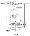
- the first memory interface network 118 which network 118 ( Figure 3) includes a compressor 138 coupled with the computer network 122 by suitable control logic circuit 140, a direct memory access (DMA) circuit 142, an image bus arbiter 144 and a burst buffer 146.
- the compressor 138 may comprise conventional components of the type suitable for use with the adaptive algorithm disclosed in US-A-4,559,563.
- the control logic 140 can comprise a known I/O device, such as the 8255 I/O port manufactured by Intel, Corp.
- One purpose of the compressor 138 is to maximize the rate at which data can be transmitted to the memory network 120. In the preferred form of operation, compression ratios of up to 30:1 have been achieved.
- the compressor 138 is coupled with the burst buffer 146 as an integrated adaptive compressor (IAC), the IAC being designated by the numeral 148.
- IAC integrated adaptive compressor
- the illustrated burst buffer 146 of Figure 3 is a "first in/first out (FIFO)" type buffer having a capacity of 64 Bytes, in other arrangements ping-pong buffers, such as the ones used in the IOT interface 46, could be substituted for the FIFO burst buffer 146.
- FIFO first in/first out
- 8 bit bytes inputted to the IAC 148 by way of bus 44 can be combined into 16 bit bytes for transmission to the memory section 120.
- the IAC 148 is interconnected with the DMA circuit 142 by a control line 150, and with the IBA 144 by way of a request line 152.
- Image data in the form of 16-bit bytes are transmitted through the memory network 120 by way of a 16 bit bi-directional image bus 154. Transmission of the image data from the IAC 148 is accomplished by use of the DMA circuit 142.
- the DMA circuit 142 includes a memory access register (MAR) 156 and a control logic circuit 158, the control logic circuit 158 being adapted to transfer image data to and from I/O components, such as the IAC 148.
- MAR memory access register
- control logic circuit 158 being adapted to transfer image data to and from I/O components, such as the IAC 148.
- programming of the MAR 156 is achieved by use of the computer network 122, and more specifically with a CPU or MPU 160.
- the MAR 156 is packaged with control logic circuit 158, and the the MAR 156 ( Figures 3 and 5) is coupled with the CPU 160 by way of a data bus 162 (PD00-PD15). Additionally, the MAR 156 and the control logic circuit 158 are coupled with the image bus arbiter 144 by way of respective control lines 163, 164.
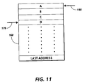
- the memory network 120 includes a memory section 166 having a page buffer 168, the page buffer 168 being interconnected with the MAR 156 by a 24-bit address bus 170, and with the control logic circuit 158 by a control line 172.
- read, write and other appropriate page buffer control signals can be transmitted across the control line 172 in response to commands transmitted by the IBA 144 to the control logic circuit 158.
- the illustrated MAR 156 includes a first address counter 178 and a second address counter 180, both of which counters 178,180 are selectively coupled with the address bus 170 by way of a 2:1 MUX 181, the MUX 181 having a tri-stated output. Additionally, a first 24-bit preloadable comparator 182 and a second 24-bit preloadable comparator 184 are respectively coupled with the address counters 178,180. Each of the comparators 182,184 is adapted to set the beginning and finishing addresses of the address counter to which it is coupled.
- Each of the counters 178,180 and the comparators 182,184 is coupled with an MPU interface 186, a control register 188, as well as a clock output and control logic circuit 190, by way of a suitable bus 192.
- the MPU interface 186 preferably comprises various control lines which permit control of the MAR 156 by the CPU 160.
- the four address lines PA1-PA4 can be used to set each internal register of the MAR 156, while the 16-bit bi-directional data bus lines of bus 162 can be used to provide control data for the control register 188.
- the control register 188 is divided into two sections, with one section being dedicated to the first counter 178, and the other section being dedicated to the second counter 180.
- the clock output and control logic circuit 190 which can provide a clock rate of up to 32 MHz, is adapted to select which of counters 178,180 is to be placed on the address bus 170 to count from one address to another.
- DRAM dynamic random access memory
- the page buffer 168 has 4 Mbytes of DRAM.
- DRAM is a relatively inexpensive alternative to static RAM.
- periodic refreshment is generally required by, for example, a conventional refresh control device (“RF controller") 196, which device 196 can be coupled with the page buffer 168 by way of the image data bus 154.
- the RF controller 196 communicates with the IBA 144 via request line 200, and with the control logic circuit 158 via a control line 202.
- a disk drive module 204 is disposed on the image data bus 154.
- the disk drive module 204 includes a disk drive 206, such as a "Winchester”-type hard disk drive with 50 Mbyte capacity, coupled with a disk drive controller ("DDC") 208.
- the module 204 communicates with the page buffer 168 via the image data bus 154, as well as with the computer network 122 via the image bus 154 and an intermediate bus 210.
- the disk drive controller 208 is coupled with the IBA 144 by way of request line 212, and with control logic circuit 158 by way of control line 214.
- the second memory interface network 124 comprises a burst buffer 216, a decompressor 218 and an 8-bit raw data bypass bus 220.
- the burst buffer 216 is structurally equivalent to the burst buffer 146, and the decompressor 218 is part of the same IC package as the compressor 138.
- the burst buffer 216 is preferably coupled with the decompressor 218 to form an integrated adaptive decompressor (IAD) 222.
- the IAD 222 is coupled with the IBA 144 by way of request line 224, and with control logic circuit 158 by way of control line 226.
- the output of the burst buffer 216 is preferably 8-bit and the decompressor 218 is on an 8-bit data bus 230.
- the output of the decompressor 184 can be transmitted to the IOT interface 46 for printing, in a known manner, at the ROS 50.
- the computer network 122 includes the CPU 160 coupled with a 16-bit CPU bus 232.
- the CPU 160 may comprise a Motorola 68020 microprocessor capable of operating at a clock frequency of 10MHz. Additionally the CPU bus 232 preferably comprises a 16-bit wide data bus, 23-bit wide address bus and control lines.
- Various types of memory namely a ROM device 234, a system RAM device 236 and an EEPROM device 238, are respectively coupled with the CPU bus 232 to support the CPU 160 in a known manner.
- a local interrupt and arbitration device 240 as well as a counter(s)/timers section 242 are coupled to the CPU bus 232 to facilitate management and operation of the CPU bus 232 in a known manner.
- an input device or data source 244 such as a workstation or another scanner can be coupled to the the CPU bus 232 so that data can be inputted to the memory section 166 concurrent with other I/O operations, such as accumulating image data in the burst buffer 146.
- a suitable interface is preferably employed to achieve suitable coupling.
- the CPU 160 can be interconnected with the IIT 12, by an IIT universal asynchronous receiving/transmitting (UART) device 246.
- the CPU 160 can use the CPU bus 232 and a request line 248 to seek access of the image data bus 154 through the IBA 144.
- the CPU 160 is coupled to the control logic circuit 158 by way of buses 134, 162 and 232.
- the CPU 160 represents the "brains" of the VP 16.
- the CPU 160 serves as an operating system for the VP 16 in that it is responsible for, among other things, system initialization, "housekeeping," system management and communication with I/O devices.
- the CPU 160 serves as a diagnostic tool for VP 16--transmitting diagnostic signals through the MUX 126 and receiving feedback signals across the buses 210, 232.
- the CPU 160 plays a major role in facilitating data transfer by way of its communication with the DMA 142 across data bus 162.
- the CPU 160 is capable of transferring data with the UI 130 and/or the page buffer 168 for manipulating image data.
- the CPU 160 has registers in which various known digital operations, such as resolution conversion and data rotation, can be performed on the image data.
- various known digital operations such as resolution conversion and data rotation
- the CPU 160 since the CPU 160 is in direct communication with the page buffer 168, by way of bus 210, the CPU 160 can transfer data with the page buffer 168 independent of the IAC 148. Consequently, data can be transferred directly between the page buffer 168 and the CPU 160 while image data is being accumulated in the burst buffer 146.
- each of the transceivers comprises a 74F245 bi-directional transceiver manufactured by Texas Instruments, Inc.
- the image data transmitted to IOT interface 46 from page buffer 168 can be printed, in a known manner, at IOT 14. Storing one or more pages of image data before printing, however, can cause some delay in printing. To eliminate such delay, the VP 16 is provided with a "direct data bus" 260, the bus 260 coupling the IIT interface 42 directly with the IOT interface 46. Accordingly, when the input rate of the IIT 12 is synchronized relative to the output rate of the IOT 14, line-by line synchronous input/output operations can be achieved.
- the sequencing role of the IBA 144 can be more fully understood.
- the IBA 144 is implemented by way of a state machine, namely a Field Programmable Array, such as the PAL 825105 manufactured by Signetics, Corporation.
- a state machine namely a Field Programmable Array, such as the PAL 825105 manufactured by Signetics, Corporation.
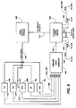
- FIG 6 the relationship of the IBA 144 to varios I/O components as well as to the control logic 158 and the page buffer 168, is shown.
- the IAD 222 transmit request signals across respective request lines 152, 248, 200, 212 and 224 to the IBA 144.
- the IBA 144 designates the order in which the above-mentioned components can access the bus 154. More specifically, the IBA 144 causes the control logic circuit 158 to by transmit an appropriate control signal across one of control lines 150, 202, 214, 226 and 250 for selectively permitting one of the above-mentioned components to access the bus 154. As the control logic circuit 158 transmits the appropriate control signal to the designated one of the above-mentioned I/O components, it also transmits information to the page buffer 168, by way of control line 172, regarding which component has been permitted access to the bus 154. It will be appreciated by those in the art that while the sequencing arrangement has been shown with five components, in other contemplated embodiments additional components could be sequenced and controlled by the arrangement of the IBA 144 and the control logic circuit 158 without altering the concept disclosed by the present description.
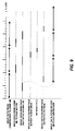
- the concept underlying the software employed to implement the IBA 144 is discussed in further detail.
- the numbered "bubbles" represent states through which a state machine can pass.
- Programming of the PAL 825105 to accomplish the software of Figure 7 is known to those skilled in the art.
- the PAL of the IBA 144 is driven by a 25 MHz clock and all input signals are synchronized with the clock so that the arbitration time is less than 40 ns.
- the priorities of the devices coupled to the IBA 144 are assigned as follows: RF 196 #1 IAC 148/IAD 222 #2 DDC 208 #3/#4 CPU 160 #3/#4
- the priorities of the RF 196 as well as IAC 148 and IAD 222 are fixed, while the priorities of the DDC 208 and the CPU 160 are rotated after each data transfer.
- the concept underlying the arbitration process is not affected by the order of priority in which the above-mentioned devices are set. Referring to Figure 7, the sequencing and rotating capacity of the IBA 144 is explained in further detail.
- the machine waits until the service routine for the RF 196 to be completed before proceeding to step 10 or 1D. Similarly, if the DDC 208 or the CPU 160 requests access to the bus 154, the machine determines whether the RF 196, the IAC 148 or the IAD 222 is being serviced before proceeding.
- the sequencing scheme of the arbitration example is elaborated on more completely in the Legend of Figure 7.
- the rotation of the IAC 148 and IAD 222 as well as the DDC 208 and the CPU 160 is achieved by the setting of a "flag."
- a request arrives for the IAC 148, the machine proceeds from states 3F to 10 and sets a flag so that the priority of the IAC 148 is set below the priority of the IAD 222. Accordingly, after the process returns to state 3F, if requests are received from IAC 148 and IAD 196 within about the same preselected time interval, the process continues through states 1D-1A rather than 10-1A. Upon proceeding to state 1D, another flag is set so that the priorities of the IAC 148 and IAD 196 are again rotated.
- the same flag setting approach can be used in servicing the DDC 208 and the CPU 160.
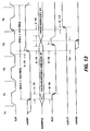
- the exemplary process begins with the CPU 160 transferring data to the page buffer 168 (active). In the time interval between a and b, the RF 196, the IAC 148, the IAD 22 and the DDC 208 request access to the bus 154. The IBA 144 waits until the CPU 160 transfer is completed and then grants the bus 154 (at time b) to the device having the highest priority, i.e. the RF 196. The IAD 148 or the IAD 222 and the DDC 208 wait until RF 196 has completed its transfer.
- the DDC 208 After the DDC 208 has accessed the bus 154 between times d and e, its priority changes to #4 and at time e the CPU 160 accesses the bus 154. After the CPU 160 has made its second transfer (between times e and f) its priority is changed to #4 and the priority of the DDC 208 is shifted back to #3. Accordingly, at time f, when a concurrent request for the bus 154 comes in from the DDC 208 and the CPU 160, access to the bus 154 is granted to the DDC 208.
- the CPU 160 Prior to transmitting an appropriate scan signal to the scanning section of IIT 12 by way of the IIT UART 246, and a print signal to the IOT interface 46, the CPU 160 communicates with the MAR 156 ( Figures 3 and 6), by way of data bus 162, to allow for the configuring of addresses in the page buffer 168, the addresses being the 24-bit locations at which image data are stored.
- the scan signal is transmitted to the scanning section of IIT 12.
- the corresponding image data is transmitted to the IAC 148, by way of the MUX 126, and to the IOT interface 46, by way of the direct data bus 260.
- each byte of image data transmitted to the IAC 148 is compressed, using the adaptive algorithm of US-A-4,559,563, and temporarily accumulated in the burst buffer 146.
- image data can be written in or read from the page buffer 168 as image data is being accumulated in the burst buffer 146.
- the IBA 144 causes the control logic circuit 158 to synchronously transmit three signals to the IAC 148, the MAR 156 and the page buffer.
- the enabling signal, nAEN1 goes low and a valid address # 1 is "pointed to" by the counter 178.
- the second signal which is transmitted across control line 150, allows the IAC 148 to access the bus 154 so that the image data byte is transferred to the designated address.
- the page buffer 168 stores the byte at the designated address.
- nAEN1 goes low, and the RDY signal goes low, the process can be repeated as many times as may be required to transfer a preselected group of bytes.
- the address counter 178 advances to the next address location in the page buffer 168 on the rising edge of nAEN1. If the data in the comparator 182 is equal to the count in the counter 178, CLR-C1 will go active active no later than 7.5 ns after the rising edge of the clock. CLR-C1 will stay active until the address in the counter 178 has been placed onto the output bus 170. Subsequently, when nAEN1 goes high, the counter 178 will be reset.
- DMA direct memory access
- up to eight (8) 16-bit bytes are accumulated in the burst buffer 146 of the IAC 148, and after buffering the eighth byte, four of the first-collected bytes are transferred to the page buffer 168 in the burst mode.
- a similar transfer scheme can be achieved for transferring image to and accumulating image data at the IAD 224.
- four bytes of image data can be transferred from the page buffer 168 to the burst buffer 216 of the IAD 222 in a burst mode for accumulation therein.
- the accumulated image data can be transferred to the IOT interface 46, by way of decompressor 218, at a rate that is substantially less than the burst mode transfer rate.
- components other than the IAC 148 and the IAD 222 can communicate with the page buffer 168 at time intervals in which image data is not being transferred to and from the page buffer 168 in the burst mode.
- the page buffer 168 there are at least three intervals in which the page buffer 168 respectively communicates with the CPU 160, the RF 196 and the DDC 208 while image data is being accumulated at the burst buffer 146 and/or image data is being transmitted to the IOT interface 46.
- image data can be transmitted to the CPU 160 for manipulation thereof, and in another example image data can be stored sequentially in the disk drive 206 for subsequent printing. It will be recognized that use of the disk drive 206 to store image data is preferred when printing of sets of multiple copies is desired.
- the compressor 138 can write image data to the burst buffer 146 at a rate of one (1) 16-bit byte per 700 ns
- the burst buffer 146 can accumulate four (4) 16-bit bytes in 2800 ns.
- the four bytes can be transferred to the page buffer 168 in 600 ns. Accordingly, during the accumulation period, 2200 ns remain for another I/O device to access the image data bus 154.
- CPU 160 400 ns/16-bit byte (at 10MHz clock)
- RF 196 400ns/16-bit byte
- DDC 208 300 ns/Refresh Cycle
- image bus utilization of the image data bus 154 can be calculated relative to the I/O device using the bus 154 with the least frequency.
- the RF 196 having a refresh cycle of 300 ns every 15000 ns, requires the bus 154 with the least frequency, i.e. only 2% of the 15000 ns interval.
- the DDC 208 requests the bus once every 5000 ns (8% of the 15000 ns interval), and, for a worst case compression ratio of 1:1, either the IAC 148 or the IAD 222 requires a data transfer once every 2800 ns for 600 ns (8% of the 15000 ns interval).
- the CPU 160 can use the bus as much as 68.57% of the 15000 ns interval.
- compression rates which in the preferred embodiment can be as high as 30:1, even more bus access time is made available for either the CPU 160, the RF 196 and the DDC 208.
- the relatively high utilization scheme described above permits for advantageous operation of the printing apparatus 10 in that multiple functions, such as data transfer, data manipulation and data storage, can all be performed in a time interval that, at least to the user, seems extremely brief.
- each of counters or pointers 178,180 ( Figure 5) function as "loop-around pointers" whose movements are respectively limited by the pre-programmed comparators 180,182. Accordingly, respective movement of each of the counters or pointers 178,180 down the stack of the page buffer 168 is limited by the respective settings of the comparators 182,184.
- Such limiting of the pointers 178,180 is particularly suitable for those instances in which the user does not intend to overwrite certain data stored further down in the stack
- Another aspect of the dual pointer arrangement is that image data need not be written into and read out of the page buffer 168 with the same counter.
- four bytes of image data have been written into the page buffer 168 from the IAC 148 so that the pointer 178 has been moved from the first address "A" to the fourth address "D.” If only pointer 178 were available, the image data would be read out of the page buffer 168 by looping the pointer 178 back to address A. With the concept disclosed herein, however, the data at the addresses A-D can be read out using the second pointer 180.
- each of pointers 178,180 can be used to designate an address for use in any suitable page buffer operation.
- the address D can be designated for a data transfer operation with a first I/O device by causing the enabling signal nAEN1 to go low.
- the address at A can be designated for a data transfer operation with a second I/O device by causing the enabling signal nAEN2 to go low.
- the first I/O device could be the IAC 148 with image data being written into the page buffer 168
- the second I/O device could be the IAD 224 with data being read out to the IOT interface 46.
- the I/O devices could be various combinations of the IAC 148, the CPU 160, the RF 196, the DDC 208, the IAD 222 or any like I/O device that could be coupled with the page buffer 168.
- the expandable ESS 300 comprises a CPU processing module 302, a DMA processing module 304 as well as an IIT/IOT module 306, a FAX 307, a video processor (VP) 308, a page description language (PDL) decomposing module 309, an image manipulation board (IMB) 310 and user interface (UI) 311.
- the processors 302 and 304 are coupled with some or all of the input/output modules 306-311 by way of three buses, the three buses being respectively referred to as CBUS 320, DBUS 322 and VBUS 324.
- each of the buses, 320,322 and 324 is a multi-purpose bus that is capable of transferring addresses, control data and image data thereacross substantially concurrently.
- the CPU processor 302 and the DMA processor 304 are respectively coupled with the CBUS 320 and the DBUS 322.
- the IIT/IOT module 306 is coupled with both the CBUS 320 and the VBUS 324.
- each of the processors 302, 304 and the modules 306-311 is coupled with one of the buses 320, 322 and 324 by way of a conventional connector 326.
- each of the input/output modules 307-311 communicates selectively with the buses 320 and 322 by way of an arrangement including one of the connectors 326 and a multiplexor 328, which multiplexor 328 is controlled across a line 330.
- the CPU processing module 302 comprises the CPU 160 and the RAM 236 as well as an I/O control block 332, a communications port 334 and a control device 336.
- the I/O control block 332 serves as an interface which allows the CPU 160 to interact with the various input/output modules 306-311 of the expandable ESS 300.
- the I/O control block 332 allows the CPU 160 to determine the timing of the FAX 308 so that addresses and/or data can be transferred appropriately between the CPU processing module 302 and the FAX 308.
- the communications port 334 which may, in one example, comprises a Centronics Port and/or a RS 232 allows the CPU processing module 302 to communicate with peripherals, such as another terminal or printer.
- Data can be transferred between the CPU 160 and modules 306-311 by way of the control device 336, the control device 336 serving as a decoder for the CPU processing module 302.
- the control device 336 serving as a decoder for the CPU processing module 302.
- the CPU 160 places the byte of data on the CBUS 320 with a suitable address, and once the address is decoded by the control device 336, the data can be transferred to the module corresponding to the address.
- the control device 336 communicates with the various components of the expandable ESS 300 by way of request and acknowledge lines respectively designated as "RQ" and "ACK.”
- the transmitting module places a request on the CBUS 320 so that the CPU 160, by use of, for example,an internal arbiter, can acknowledge the transfer of the byte of data to the RAM 236.
- the DMA processing module 304 comprises a DMA module 340, a LAN module 342, a Disk Drive module 344 and a control device 346.
- the DMA module 340 comprises a known DMA device, such as one of the DMAs manufactured by Simpson or Motorola Corporations, coupled to the DBUS 322 by way of a DMA controller, the DMA controller being adapted for use with the various components of the expandable ESS 300.
- the general concepts underlying the structure and operation of the DMA module 340 can be more fully appreciated by reference to Figures 3A, 3B and the accompanying discussion of the DMA 142.
- the LAN module 342 is shown in further detail.
- the LAN module 342 comprises a LAN system 348 and a controller 350 for interfacing the LAN system 348 with the DBUS 322.
- the LAN system 348 includes an Ethernet LAN 349 to which a number of work stations 352 are connected.
- Workstation 352 may be, for example, the Xerox 6085 professional work stations.
- LAN 349 may also have other office connected equipment, such as a network file server 354, a network file mail communication server 356, a print server 358 and an electronic printer 360. Also, a large capacity remote storage facility, such as a mini-computer 362 may be connected to the LAN 349.
- the LAN system 348 is a collaborative system, meaning that it enables users at different workstations 352 to work together in real-time by processing and passing information among one another and storing and retrieving information from storage services 354 and 362 via the network 349.
- the Disk Drive module 344 ( Figure 13) comprises one or more disk memory devices 366, which devices 368 are coupled with the DBUS 322 by way of a disk drive controller 368, such as a SCSI controller.
- a disk drive controller 368 such as a SCSI controller.
- the control device 346 functions in the same manner as the control device 336. That is the control device 346 decodes addresses for data transferred across the DBUS 322. Additionally, the control device 346 communicates with the various components of the expandable ESS 300 by way of request and acknowledge lines respectively designated as "RQ" and "ACK.”
- the CPU processing module 302 and the DMA processing module 304 share a system RAM 370.
- the system RAM 370 serves as a global storage area for software and files used with the various components of the expandable ESS 300.
- the system RAM 370 is particularly well suited to store wide variety software, such as image conversion and image editing software, for use with the CPU 160.
- the IIT/IOT module 306 is constructed with the above-discussed components.
- the IIT 12 and the IOT 14 are respectively coupled with IIT interface 42 and IOT interface 46.
- the FAX 307 is a conventional group III type facsimile device, which may be similar in construction to the illustrated FAX of US-A-5,021,892.
- the FAX 307 may include a transmission control portion (not shown), the control portion containing a slave CPU (not shown) for controlling a data transmission procedure based on a CCITT standard.
- the control portion is adapted to exchange data with any of the buses 320, 322 and 324 according to the transmission procedure.
- the control portion can also be connected to a telephone line by way of a modem (not shown) and a network control unit (not shown) as shown in the '892 patent.
- the video processor (VP) module 308 incorporates many of the basic components of the VP 10, the VP 10 being discussed in further detail above. More specifically, the VP module 308 can be implemented with various components of networks 116, 118, 120 and 124 to achieve such functions as data compression, relatively high speed data transfer, image bus arbitration, image data storage and data decompression
- the page description language (PDL) decomposing-processing module 309 comprises all of the necessary hardware, such as a dedicated processor and suitable registers, to decompose a master PDL file into a bitmap file for printing.
- PDLs are an interchange standard for representing documents electronically within a system and ultimately printing those documents.
- documents formatted as a PDL file can be exchanged between the work stations 352 of the LAN system 348, the PDL processing module 309 and the IOT 14 in an efficient and consistent manner.
- the PDL file describes, among other things, how images are to be rendered on each page, what font is to be employed and how the pages are to be assembled.
- the PDL processing module 309 can receive, as input for printing, electronic documents in various forms, such as POSTSCRIPT, HP-PCL or INTERPRESS.
- the image manipulation board (IMB) 310 comprises suitable hardware for achieving such functions as image editing and image conversion.
- the hardware may comprise a dedicated processor and a suitably sized bitmap, the bitmap being adapted for use with a large variety of software.
- the IMB 310 is particularly suited for, among other procedures, wide and small angle rotations, image annotation, or any other known image manipulation processes.
- User Interface (UI) module 311 can possess the same structure as that discussed above for user interface 130 ( Figures 3A, 3B). In the illustrated embodiment of Figure 13, the user interface module 311 is adapted for use with a conventional terminal 372. Additionally, as above, the user interface 130 is coupled with the buses 320, 322 and 324 by way of suitable interface logic, such as user interface logic 132.
- the expandable ESS 300 operates as a multi-tasking arrangement capable of performing simultaneous or concurrent operations.
- the modules 306-311 communicate with the VBUS 324, addresses, image data and control data can be communicated between any of the two modules 306-311.
- each of the modules 306-311 is coupled with the CBUS 320 addresses, control data and image data can be transferred between the CPU processing unit 302 and any one of the modules 306-311 that is not using the VBUS 324. That is, transfers across the VBUS 324 between two of modules 306-311 can be performed concurrently with transfers between the CPU processing module 302 and the one of the modules 306-311 which is not using the VBUS 324.
- modules 307-311 are coupled with the DBUS 322, data can be transferred between the LAN module 342 or the disk drive 344 and any one of the modules 307-311 which is not using the buses 320 and 324.
- large blocks of data can be transferred from or to either the LAN module 342 or the disk drive 344 relatively quickly by use of the DMA module 340.
- data transfer can be performed concurrently with data transfers on the CBUS 320 and the VBUS 324.
- image data is transferred between the IMB 310 and the IIT/IOT interface 306 concurrently with transfers between both the CPU processing module 302 and the FAX 307 and between the disk drive module 344 and the PDL processing module 309.
- concurrent transfers can be achieved using various combinations of the CPU processing module 302, the DMA processing module 304 and the input/output modules 306-311.
- the use of three buses 320, 322 and 324, in conjunction with the processors 302, 304 and the input/output modules 306-311 allows for up to three simultaneous transfers.
- additional buses as well as additional processors and additional input/output modules could be employed to achieve a higher degree of flexibility with more than three concurrent transfers.
- One particular feature of the described printing machine is that it is characterized by an exceedingly high level of concurrency in that it enables three separate sets of data to be substantially concurrently transferred across three separate multipurpose buses.
- Another feature of the described printing machine is that various subsystems, such as an IIT/IOT arrangement, a video processor, a facsimile apparatus, an image manipulation board, a page description language module and a user interface, can be respectively incorporated into discrete modular stand-alone units, each of which modular units can be added to or omitted from the printing machine in accordance with the user's desires. That is, in accordance with the user's specifications, the machine can be designed to range from simple to complex. Additionally, since each module can operated with its own dedicated software, timing dependency of the printing machine on a single system manager is decreased significantly.
- Yet another feature of the described printing machine is that it possesses a particularly flexible design. Accordingly a user can obtain a machine that not only provides a wide variety of functions through the use of the stand-alone input/output modules, but is capable of interfacing with, among other systems, a local area network.
Landscapes
- Engineering & Computer Science (AREA)
- Multimedia (AREA)
- Signal Processing (AREA)
- Computer Hardware Design (AREA)
- Microelectronics & Electronic Packaging (AREA)
- General Engineering & Computer Science (AREA)
- Physics & Mathematics (AREA)
- General Physics & Mathematics (AREA)
- Theoretical Computer Science (AREA)
- Record Information Processing For Printing (AREA)
- Accessory Devices And Overall Control Thereof (AREA)
- Control Or Security For Electrophotography (AREA)
- Fax Reproducing Arrangements (AREA)
Applications Claiming Priority (2)
| Application Number | Priority Date | Filing Date | Title |
|---|---|---|---|
| US784195 | 1991-10-29 | ||
| US07/784,195 US5276799A (en) | 1991-10-29 | 1991-10-29 | Expandable electronic subsystem for a printing machine |
Publications (1)
| Publication Number | Publication Date |
|---|---|
| EP0540176A1 true EP0540176A1 (fr) | 1993-05-05 |
Family
ID=25131648
Family Applications (1)
| Application Number | Title | Priority Date | Filing Date |
|---|---|---|---|
| EP92308882A Withdrawn EP0540176A1 (fr) | 1991-10-29 | 1992-09-29 | Sous-système électronique expansible pour imprimeur |
Country Status (3)
| Country | Link |
|---|---|
| US (1) | US5276799A (fr) |
| EP (1) | EP0540176A1 (fr) |
| JP (1) | JPH05278304A (fr) |
Cited By (2)
| Publication number | Priority date | Publication date | Assignee | Title |
|---|---|---|---|---|
| EP0869428A3 (fr) * | 1997-04-02 | 1999-10-06 | Canon Kabushiki Kaisha | Système et appareil de traitement d'image |
| EP1292109A1 (fr) * | 2001-08-27 | 2003-03-12 | Ricoh Company, Ltd. | Système de traitement d'information |
Families Citing this family (46)
| Publication number | Priority date | Publication date | Assignee | Title |
|---|---|---|---|---|
| WO1993017875A1 (fr) * | 1992-03-02 | 1993-09-16 | Seiko Epson Corporation | Dispositif de commande supplementaire, et appareil et methode de traitement des informations relatives a ce dispositif |
| WO1993018922A1 (fr) * | 1992-03-19 | 1993-09-30 | Seiko Epson Corporation | Appareil et procede de traitement d'informations, et dispositif de commande supplementaire utilise |
| JPH0670076A (ja) * | 1992-08-19 | 1994-03-11 | Toshiba Corp | ファクシミリ蓄積交換システム |
| US5459818A (en) * | 1992-11-02 | 1995-10-17 | Hewlett-Packard Company | Display list with crossing queues |
| US5420696A (en) * | 1993-06-24 | 1995-05-30 | Xerox Corporation | Image data transfer architecture and method for an electronic reprographic machine |
| US5528375A (en) * | 1994-04-20 | 1996-06-18 | Xerox Corporation | Apparatus for and method of scheduling and printing a job in a printing machine |
| US5469534A (en) * | 1994-06-14 | 1995-11-21 | Xerox Corporation | Method for translating image processing data |
| US5493635A (en) * | 1994-06-14 | 1996-02-20 | Xerox Corporation | System for combining heterogeneous image processing jobs into a single job |
| US5600762A (en) * | 1994-09-29 | 1997-02-04 | Xerox Corporation | Method of processing a job, in a printing system, with a composite job ticket |
| US5659634A (en) * | 1994-09-29 | 1997-08-19 | Xerox Corporation | Apparatus and method for encoding and reconstructing image data |
| US5710873A (en) * | 1994-09-29 | 1998-01-20 | Xerox Corporation | Apparatus and method for maximizing a rate of image data transfer in a printing system |
| JPH08115414A (ja) * | 1994-09-29 | 1996-05-07 | Xerox Corp | 差込み/注釈付け/背丁付け能力を有する印刷機械 |
| US5579452A (en) * | 1994-09-29 | 1996-11-26 | Xerox Corporation | Method of managing memory allocation in a printing system |
| US5682467A (en) * | 1994-09-29 | 1997-10-28 | Xerox Corporation | Arbitrating apparatus for controlling selective access of multiple bus masters to a printing system video bus |
| US5602974A (en) * | 1994-10-05 | 1997-02-11 | Microsoft Corporation | Device independent spooling in a print architecture |
| US6243172B1 (en) * | 1995-01-18 | 2001-06-05 | Varis Corporation | Method and system for merging variable text and images into bitmaps defined by a page description language |
| US5729665A (en) * | 1995-01-18 | 1998-03-17 | Varis Corporation | Method of utilizing variable data fields with a page description language |
| US5619649A (en) * | 1995-06-12 | 1997-04-08 | Xerox Corporation | Network printing system for programming a print job by selecting a job ticket identifier associated with remotely stored predefined document processing control instructions |
| US5687297A (en) * | 1995-06-29 | 1997-11-11 | Xerox Corporation | Multifunctional apparatus for appearance tuning and resolution reconstruction of digital images |
| US5796930A (en) * | 1995-11-13 | 1998-08-18 | Varis Corporation | System architecture for processing and transporting page-map or bit-map data to a raster print engine |
| US6003007A (en) * | 1996-03-28 | 1999-12-14 | Dirienzo; Andrew L. | Attachment integrated claims system and operating method therefor |
| US9619841B2 (en) | 1996-03-28 | 2017-04-11 | Integrated Claims Systems, Llc | Systems to assist in the creation, transmission, and processing of health insurance claims |
| JPH10198229A (ja) * | 1996-12-30 | 1998-07-31 | Canon Inc | 画像処理装置および方法 |
| JPH10333977A (ja) * | 1997-05-28 | 1998-12-18 | Oki Electric Ind Co Ltd | マイクロコントローラ装置 |
| US6487568B1 (en) * | 1997-07-18 | 2002-11-26 | Tesseron, Ltd. | Method and system for flowing data to an arbitrary path defined by a page description language |
| US7302438B1 (en) | 1997-07-18 | 2007-11-27 | Tesseron Ltd. | Method and system for flowing data to an arbitrary path defined by a page description language |
| US6353899B1 (en) * | 1998-04-10 | 2002-03-05 | Xerox Corporation | Fault management system for a multifunctional printing machine |
| US6266153B1 (en) | 1998-05-12 | 2001-07-24 | Xerox Corporation | Image forming device having a reduced toner consumption mode |
| JP3305265B2 (ja) | 1998-07-24 | 2002-07-22 | キヤノン株式会社 | 画像処理装置およびその方法 |
| US7315979B1 (en) | 1998-11-09 | 2008-01-01 | Tesseron Ltd. | Method and system for dynamic flowing data to an arbitrary path defined by a page description language |
| JP2000211216A (ja) * | 1999-01-25 | 2000-08-02 | Canon Inc | 複合機器の情報処理方法及びシステム |
| US6439706B1 (en) * | 1999-05-25 | 2002-08-27 | Silverbrook Research Pty Ltd. | Printer cartridge with binder |
| JP2000339008A (ja) * | 1999-05-27 | 2000-12-08 | Hitachi Ltd | プログラマブルコントローラ |
| US6570670B1 (en) | 1999-11-29 | 2003-05-27 | Xerox Corporation | Method and apparatus to enable job streaming for a set of commonly shared resources |
| US6651081B1 (en) | 1999-11-29 | 2003-11-18 | Xerox Corporation | Method and apparatus for processing a high priority resource request in a system using a set of shared resources |
| US6762857B1 (en) | 1999-11-29 | 2004-07-13 | Xerox Corporation | Method and apparatus to enable processing multiple capabilities for a sub-job when using a set of commonly shared resources |
| US6614542B1 (en) | 1999-11-29 | 2003-09-02 | Xerox Corporation | Method and apparatus to improve system concurrency for a job using a set of commonly shared resources such that a specific resource is used only for a portion of the job |
| US6671065B1 (en) | 1999-11-29 | 2003-12-30 | Xerox Corporation | Method and apparatus to optimize transition of resources from a lower priority to a higher priority job |
| US6717690B1 (en) | 1999-11-29 | 2004-04-06 | Xerox Corporation | Method and apparatus for managing job contention for system resources in an electrographic reproduction system where images are multibanded |
| US6501559B1 (en) | 1999-11-29 | 2002-12-31 | Xerox Corporation | Method and apparatus for managing job contention for system resources in an electronic reprographic system |
| US6463481B1 (en) | 1999-12-02 | 2002-10-08 | Xerox Corporation | Direct memory access control system for a digital scanner |
| US6738158B1 (en) | 1999-12-02 | 2004-05-18 | Xerox Corporation | Digital scanner for capturing and processing images |
| US6401143B1 (en) | 1999-12-02 | 2002-06-04 | Xerox Corporation | Loopback direct memory access control system for a digital scanner |
| US6509978B1 (en) * | 2000-02-25 | 2003-01-21 | Eastman Kodak Company | Method and apparatus for formatting bitmapped image data |
| US6665098B1 (en) | 2000-02-28 | 2003-12-16 | Xerox Corporation | Dynamic user interface based on frequency of user settings |
| US7529823B2 (en) * | 2003-03-27 | 2009-05-05 | Microsoft Corporation | Notifications for shared resources |
Citations (4)
| Publication number | Priority date | Publication date | Assignee | Title |
|---|---|---|---|---|
| US3644901A (en) * | 1969-07-24 | 1972-02-22 | Univ Iowa State | Digital system for controlling signal transfers between registers and data buses |
| GB2166620A (en) * | 1984-11-02 | 1986-05-08 | Ricoh Kk | Facsimile apparatus |
| EP0193980A1 (fr) * | 1985-03-01 | 1986-09-10 | Hollandse Signaalapparaten B.V. | Réseau local utilisant un système de bus multiple |
| EP0262603A2 (fr) * | 1986-09-30 | 1988-04-06 | Sharp Kabushiki Kaisha | Dispositif multifonctionnel de traitement d'images |
Family Cites Families (16)
| Publication number | Priority date | Publication date | Assignee | Title |
|---|---|---|---|---|
| US4169275A (en) * | 1977-03-10 | 1979-09-25 | Xerox Corporation | Reproduction scanning system having intermediate storage between input and output scanning stations |
| US4205350A (en) * | 1977-03-10 | 1980-05-27 | Xerox Corporation | Reproduction scanning system having intermediate storage between input and output scanning stations |
| JPS57181260A (en) * | 1981-05-01 | 1982-11-08 | Canon Inc | Picture information outputting method |
| US4672186A (en) * | 1981-10-01 | 1987-06-09 | Banctec Inc. | Digital document scanning system |
| JPS6084672A (ja) * | 1983-10-17 | 1985-05-14 | Canon Inc | 画像処理方法 |
| US4800431A (en) * | 1984-03-19 | 1989-01-24 | Schlumberger Systems And Services, Inc. | Video stream processing frame buffer controller |
| US4748662A (en) * | 1984-12-21 | 1988-05-31 | Kabushiki Kaisha Toshiba | Apparatus having a dial calling function |
| JPS63146566A (ja) * | 1986-12-09 | 1988-06-18 | Ricoh Co Ltd | デジタル複写機 |
| JPS6436374A (en) * | 1987-07-31 | 1989-02-07 | Ricoh Kk | Image retrieval system |
| US4987529A (en) * | 1988-08-11 | 1991-01-22 | Ast Research, Inc. | Shared memory bus system for arbitrating access control among contending memory refresh circuits, peripheral controllers, and bus masters |
| US4947345A (en) * | 1989-07-25 | 1990-08-07 | Xerox Corporation | Queue management system for a multi-function copier, printer, and facsimile machine |
| US5177737A (en) * | 1990-01-02 | 1993-01-05 | At&T Bell Laboratories | Multipurpose bus system |
| US5170266A (en) * | 1990-02-20 | 1992-12-08 | Document Technologies, Inc. | Multi-capability facsimile system |
| US5027221A (en) * | 1990-10-10 | 1991-06-25 | Fuji Xerox Co., Ltd. | Digital image recording system with preset control for selecting output formats based on the selected amount of pixel color and density data |
| US5038218A (en) * | 1990-10-10 | 1991-08-06 | Fuji Xerox Co., Ltd. | Image processing assembly with conversion and rotation of input image data or predetermined data to match data resolution and orientation |
| US5130809A (en) * | 1991-05-06 | 1992-07-14 | Fuji Xerox Co., Ltd. | Electrophotographic copier with constant rate data compression and simultaneous storage and decompression of compressed data received on a mutually coupled data bus |
-
1991
- 1991-10-29 US US07/784,195 patent/US5276799A/en not_active Expired - Fee Related
-
1992
- 1992-09-29 EP EP92308882A patent/EP0540176A1/fr not_active Withdrawn
- 1992-10-23 JP JP4286431A patent/JPH05278304A/ja not_active Withdrawn
Patent Citations (4)
| Publication number | Priority date | Publication date | Assignee | Title |
|---|---|---|---|---|
| US3644901A (en) * | 1969-07-24 | 1972-02-22 | Univ Iowa State | Digital system for controlling signal transfers between registers and data buses |
| GB2166620A (en) * | 1984-11-02 | 1986-05-08 | Ricoh Kk | Facsimile apparatus |
| EP0193980A1 (fr) * | 1985-03-01 | 1986-09-10 | Hollandse Signaalapparaten B.V. | Réseau local utilisant un système de bus multiple |
| EP0262603A2 (fr) * | 1986-09-30 | 1988-04-06 | Sharp Kabushiki Kaisha | Dispositif multifonctionnel de traitement d'images |
Non-Patent Citations (1)
| Title |
|---|
| PATENT ABSTRACTS OF JAPAN vol. 3, no. 156 (E-161)21 December 1979 & JP-A-54 137 941 ( NEC CORP ) 26 October 1979 * |
Cited By (4)
| Publication number | Priority date | Publication date | Assignee | Title |
|---|---|---|---|---|
| EP0869428A3 (fr) * | 1997-04-02 | 1999-10-06 | Canon Kabushiki Kaisha | Système et appareil de traitement d'image |
| US6384928B2 (en) | 1997-04-02 | 2002-05-07 | Canon Kabushiki Kaisha | Image processing apparatus and system |
| EP1292109A1 (fr) * | 2001-08-27 | 2003-03-12 | Ricoh Company, Ltd. | Système de traitement d'information |
| US7318083B2 (en) | 2001-08-27 | 2008-01-08 | Ricoh Company, Ltd. | Information processing system |
Also Published As
| Publication number | Publication date |
|---|---|
| US5276799A (en) | 1994-01-04 |
| JPH05278304A (ja) | 1993-10-26 |
Similar Documents
| Publication | Publication Date | Title |
|---|---|---|
| US5276799A (en) | Expandable electronic subsystem for a printing machine | |
| EP0552565B1 (fr) | Processeur auxiliaire d'entrée/sortie pour une machine d'impression | |
| US5261047A (en) | Bus arbitration scheme for facilitating operation of a printing apparatus | |
| US5303341A (en) | Video processor for a printing apparatus | |
| US5142667A (en) | Resource and memory management algorithms for electric printing and electronic reprographic systems | |
| EP0410668B1 (fr) | Procédé pour la gestion de files d'attente | |
| US5615314A (en) | Interface for providing rasterized data to an imaging device | |
| US6757447B2 (en) | Image manipulation for a digital copier which operates on a block basis | |
| US5659634A (en) | Apparatus and method for encoding and reconstructing image data | |
| US5218456A (en) | Disk bandwidth allocations to prioritize disk requests | |
| US5243439A (en) | Image relocation in an electronic reprographic system | |
| US6449064B1 (en) | Method and apparatus for image formation that can handle simultaneously input data without causing a delay | |
| US6298404B1 (en) | Digital copier with an unified memory which stores computer instructions and image data | |
| US5212566A (en) | Synchronization of ess/iit when scanning complex documents | |
| US5495339A (en) | Scheduling multiple disk requests and writing data buffers to disk | |
| US6463481B1 (en) | Direct memory access control system for a digital scanner | |
| US7710613B2 (en) | Image information apparatus | |
| US20040190037A1 (en) | Image processing apparatus, image processing method, and storage medium | |
| US6401143B1 (en) | Loopback direct memory access control system for a digital scanner | |
| JPH10210251A (ja) | 画像メモリアクセス方法、画像形成装置、画像形成記憶装置、アドレス発生方法、及びアドレス発生装置 | |
| JP3618420B2 (ja) | 画像形成装置 | |
| US6304927B1 (en) | Digital copier with scalable architecture | |
| US20050231764A1 (en) | Image forming apparatus for managing temporarily stored data | |
| US5200960A (en) | Streaming tape diagnostic | |
| EP0465179A2 (fr) | Appareils de copie/d'impression électroniques |
Legal Events
| Date | Code | Title | Description |
|---|---|---|---|
| PUAI | Public reference made under article 153(3) epc to a published international application that has entered the european phase |
Free format text: ORIGINAL CODE: 0009012 |
|
| AK | Designated contracting states |
Kind code of ref document: A1 Designated state(s): DE FR GB |
|
| 17P | Request for examination filed |
Effective date: 19931105 |
|
| 17Q | First examination report despatched |
Effective date: 19951213 |
|
| 18W | Application withdrawn |
Withdrawal date: 19960424 |