EP0540899B1 - UHF-Yagi-Antenne - Google Patents
UHF-Yagi-Antenne Download PDFInfo
- Publication number
- EP0540899B1 EP0540899B1 EP19920117301 EP92117301A EP0540899B1 EP 0540899 B1 EP0540899 B1 EP 0540899B1 EP 19920117301 EP19920117301 EP 19920117301 EP 92117301 A EP92117301 A EP 92117301A EP 0540899 B1 EP0540899 B1 EP 0540899B1
- Authority
- EP
- European Patent Office
- Prior art keywords
- antenna
- circuit board
- uhf
- circuit
- vhf
- Prior art date
- Legal status (The legal status is an assumption and is not a legal conclusion. Google has not performed a legal analysis and makes no representation as to the accuracy of the status listed.)
- Expired - Lifetime
Links
Images


Classifications
-
- H—ELECTRICITY
- H01—ELECTRIC ELEMENTS
- H01Q—ANTENNAS, i.e. RADIO AERIALS
- H01Q23/00—Antennas with active circuits or circuit elements integrated within them or attached to them
-
- H—ELECTRICITY
- H01—ELECTRIC ELEMENTS
- H01Q—ANTENNAS, i.e. RADIO AERIALS
- H01Q19/00—Combinations of primary active antenna elements and units with secondary devices, e.g. with quasi-optical devices, for giving the antenna a desired directional characteristic
- H01Q19/28—Combinations of primary active antenna elements and units with secondary devices, e.g. with quasi-optical devices, for giving the antenna a desired directional characteristic using a secondary device in the form of two or more substantially straight conductive elements
- H01Q19/30—Combinations of primary active antenna elements and units with secondary devices, e.g. with quasi-optical devices, for giving the antenna a desired directional characteristic using a secondary device in the form of two or more substantially straight conductive elements the primary active element being centre-fed and substantially straight, e.g. Yagi antenna
Definitions
- the invention relates to a UHF-Yagi antenna consisting of director elements, a reflector and a dipole.
- a Yagi antenna is already known from German Offenlegungsschrift No. 21 38 384, the known antenna being implemented in the manner of printed circuit technology and in particular in stripline technology.
- a room antenna for different frequency ranges is already known from German Offenlegungsschrift No. 24 53 164 and from the catalog "Kathrein catalog receive antennas 1990" (page 29, antenna BZX 20).
- This antenna is used to receive UHF and VHF, the UHF antenna being designed as a Yagi antenna.
- a dielectric circuit board is arranged, which receives an amplifier, switches and other electronic components. The amplifier is thus separated from the Yagi antenna by a distance that corresponds to the height of the standpipe of the Yagi antenna.
- a miniature television antenna is already known from German Offenlegungsschrift No. 2 146 182 (corresponding to US Patent 3, 707, 681).
- This known antenna has a first insulating substrate (11) on which the electrical components of the antenna are printed and a second insulating substrate (77) on which the components of the amplifier (40) are attached.
- the insulating substrate (77) with the components of the amplifier is held by a holder arm (76) which rigidly attaches the amplifier circuit to the lower housing part (62).
- the antenna and amplifier are therefore not arranged on the same substrate (circuit board); rather, in the vicinity of the substrate (11) on which the electrical components of the antenna are printed, the substrate (77 is fastened via the holding arm 76), the substrates (11) and (77) being separated from one another by a space.
- These constructive measures are apparently aimed at electromagnetically decoupling the antenna and amplifier.
- Electromagnetic decoupling proves to be critical, especially with Yagi antennas, because of the possible interaction between amplifier and antenna reflector.
- This arrangement known from German Offenlegungsschrift No. 2 146 182 is initially associated with the disadvantage that two different substrates, namely the substrate (11) for the actual antenna and the substrate (77) for the amplifier circuit, are used.
- the invention has for its object to provide a UHF Yagi antenna of the type mentioned, which enables a compact structure.
- a UHF-Yagi antenna consists of director elements, reflector and dipole, the director elements and the dipole consisting of conductor tracks. printed on a dielectric circuit board, and wherein a first Amplifier circuit is connected to the conductor tracks forming the dipole.
- the first amplifier circuit and the conductor tracks forming the dipole are arranged on the same circuit board in close proximity to one another and on the same side of the circuit board.
- the reflector is concavely curved and the first amplifier circuit is arranged between the dipole and the reflector.
- the arrangement of the amplifier and the conductor tracks on the same circuit board reduces the dimensions of the antenna and improves its electrical properties. At the same time, the manufacture of the antenna is simplified since the antenna elements and, for example, conductor tracks of the amplifier circuit can be applied to the circuit board in one operation.
- the concavely curved design of the reflector makes it possible to arrange an amplifier circuit in the space between the reflector and the dipole. This results in a compact structure and favorable electrical properties.
- By arranging the amplifier circuit in the immediate vicinity of the antenna a maximum of the energy absorbed by the antenna is used.
- a cable for connecting the UHF antenna and amplifier is not required. Mismatches and switch-on or fade-in losses are avoided, which occur when using a longer connecting line or a cable between the antenna and amplifier could result.
- the antenna according to the invention with the integrated amplifier circuit has a gain of 31 ⁇ 2 dB.
- a further advantageous embodiment is characterized in that a second amplifier circuit is arranged on the circuit board and has a connection for a VHF antenna in the form of two rods. This antenna can be installed by the consumer without the need for assembly tools.
- An antenna according to the invention in which the circuit board can be rotated, enables the antenna to be perfectly aligned in the directions of the signals to be received.
- Another embodiment of the antenna according to the invention in which the first and second amplifier circuits are followed by a mixer circuit which mixes UHF and VHF signals, is distinguished by the advantage that the UHF and VHF signals are provided in mixed form at the output thereof, whereby only one cable has to be provided for both the UHF antenna and the VHF antenna.
- the mixer circuit can be arranged on the circuit board, with which the advantages mentioned of reducing the dimensions of the overall arrangement and simplifying its assembly can be achieved to a greater extent.
- an antenna in which the circuits arranged on the circuit board are at least partially implemented in stripline technology and / or in SMD technology. This facilitates the manufacture of the overall arrangement antenna and associated electronic circuits, by printing the conductor tracks of the antenna and simultaneously printing the circuit structure of the circuits in a single process.
- the reflector consists of a double, metallic rod which forms a plane which is arranged approximately at right angles to the circuit board.
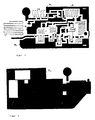
- FIG. 1 shows the position of a dielectric plate or circuit board 1 within a housing 2.
- the dielectric plate is in an inclined position of 2 degrees with respect to the horizontal plane defined by the foot part 21 of the housing 2.
- Director elements and the dipole of a UHF-Yagi antenna are arranged on the plate 1.
- the director elements and / or the dipole are formed by conductor tracks 11 which are printed on the plate 1.
- the plate 1 with the conductor tracks 11 either faces the upper part 22 of the housing 2 or the lower part 21 of the housing 2.
- the first three conductor tracks 111, 112 and 113 form the director elements and the two following conductor tracks 114 and 115 form the dipole.
- the reflector of the antenna is formed by a metal strip 12 which is arranged in a plane perpendicular to the plane in which the conductor tracks 111, 112, 113, 114 and 115 are arranged.
- the reflector can also be formed by a conductor track which is printed on the plate 1 (FIG. 2). At least one UHF amplifier circuit is arranged between the printed conductor tracks 11 and the reflector 12, as will be described with reference to FIG. 2.
- the housing 2 consists of a lower part 21 and an upper part 22.
- the shape of the housing 2 is slightly curved.
- Both parts 21 and 22 of the housing have mechanical connecting elements such as, for example, fastening pins, which enable the housing to be opened and closed easily.
- the plate 1 can be rotated in a plane parallel to the antenna base.
- the housing 2 can be connected to a carrier system 3, which is formed, for example, by a ball socket, the upper edge 31 of which is inserted into a circular groove 221 which is arranged in the lower part 21 of the housing 2 and which rotates with respect to the fixed carrier 3 allowed.
- the housing 2 is fastened to the carrier 3 by means of a screw which is inserted into an opening 32 in the base of the carrier 3, engages in a thread in a tube 212 arranged in the part 21 of the housing and extends up to within the carrier 3 whose lower base extends.
- a screw which is inserted into an opening 32 in the base of the carrier 3, engages in a thread in a tube 212 arranged in the part 21 of the housing and extends up to within the carrier 3 whose lower base extends.
- In the upper part 22 of the housing 2 there are two openings 221 into which a VHF antenna can be inserted. This consists of two rods, for example telescopic rods, which are described with reference to FIG. 7.
- the entire supply system can be arranged in the carrier 3, while a first amplifier circuit and optionally a second amplifier circuit are arranged on the plate 1 (FIG. 2).
- Figure 2 shows a schematic representation of the antenna and the associated electronic circuits. It should be noted that Figure 2 does not show the actual dimensions.
- the electronic circuit arrangements shown in FIG. 2 are at least partially implemented in microstrip technology and / or in SMD (Surface Mounting Devices) technology, so that the dimensions can be reduced very much, with an area of 75 mm in the specific embodiment ⁇ 35 mm is claimed.
- SMD Surface Mounting Devices
- the conductor tracks 111, 112, 113 and 114 have a width of approximately 3.5 mm; the conductor track 115 has a width of approximately 5 mm.
- the conductor track 111 has a length of approximately 107 mm; tracks 112 and 113 have a length of approximately 122 mm and tracks 114 and 115 have a length of approximately 92 mm and 76 mm, respectively.
- the approximate distances between the conductor tracks are as follows: the distance between the conductor tracks 111 and 112 is approximately 35 mm, the distance between the conductor tracks 112 and 113 is 16 mm and the distance between the conductor tracks 113 and 114 is 35 mm.
- the angle between tracks 114 and 115 is approximately 20 degrees.
- the reflector 12 has a parabolic shape and consists either of a conductor track which is arranged on the plate 1 (FIG. 1) or of a metal strip 12 which is in a plane perpendicular to the plane of the conductor tracks 111, 112, 113, 114, 115 is arranged.
- the conductor track has a width of approximately 3.5 mm, while the metal strip has an approximate height of 10 mm and a thickness of 0.4 mm.
- the length of the reflector (points E and F) is approximately 280 mm.
- the distance between the center of the dipole (conductor tracks 114, 115, point C) and the vertex of the parabola of the reflector (point D) is approximately 80 mm.
- the conductor tracks are made of copper, which is printed on a plate made of fiberglass. Another embodiment of the reflector is shown in FIG.
- FIG. 2 shows a first amplifier circuit which amplifies the UHF signals received by the antenna.
- a bandpass filter is arranged, which for example consists of the capacitors C23, C24, C25, C26 and C27 with 18 pF, 470pF, 1pF, 33 pF and 2.7 pF and coils L1 and L3 with 20 nH and 18 nH.
- This bandpass filter matches the impedance of the UHF antenna to the impedance of the first stage of the first amplifier circuit.
- the antenna impedance is approximately 300 ohms.
- the first amplifier consists of two transistors T1 (type NE68133 NEC) and T2 (type BFR 93A Philips). These transistors form two stages, which are matched and tuned to one another in a frequency range from 470 to 860 MHz, and cause an increase in the gain within the desired frequency band (470-860 MHz), whereby the signals are suppressed outside the frequency band.
- the first stage of the UHF amplifier is not powered with the aim of not degrading the noise characteristic, which noise characteristic is less than 2 dB.
- the second stage of the UHF amplifier is fed in order to compensate for the difference in gain as a function of the frequency generated in the first stage. This achieves a flat characteristic in the entire useful frequency range (470 - 860 MHz).
- the first amplifier circuit consists, for example, of the following components: a circuit for polarizing the transistor T1, which consists of the resistors R10, R14 and R15 with 560 ohms, 37 kiloohms and 3.3 kilohms, from a circuit for polarizing the transistor T2, which consists of resistors R7, R8, R9 and R12 with the values 470 ohms, 470 ohms, 18 kilohms and 10 kilohms; from a feedback circuit to transistor T2, which consists of resistors R11 and R13 with the values 220 ohms and 15 ohms and from the capacitors C14 and C17 with 22 pF and 470 pF, respectively, from high-pass filters consisting of the capacitor C9 and the coil L8 with 180 pF or 11nH consists of the capacitor C13 and the coil L7 with 4.7 pF or 10 nH and finally a high-
- FIG. 2 also shows a second amplifier circuit which amplifies the VHF signals received by the VHF antenna (FIG. 7).
- this amplifier which is connected directly to the VHF antenna (point I)
- a notch filter that blocks FM signals (87-108 MHz) and a low pass.
- the notch filter consists of the capacitors C29, C22, C30, C31 and C32 with the values 3.9 pF, 15 pF, 120 pF, 120 pF and 1.5 pF
- the low-pass filter consists of the coil L2 with 32 nH and the capacitor C33 with 8.2 pF.
- This low-pass filter makes it possible to match the impedance of the VHF antenna to the impedance of the second amplifier.
- the impedance of the VHF antenna is approximately 300 ohms.
- the second amplifier consists of a transistor T3 (type BFR93A Philips). This transistor is fed back in order to obtain a flat characteristic in the frequency range of 47-230 MHz.
- the second amplifier circuit consists of the following components: a polarization circuit consisting of resistors R4, R16, R2 and R1 with 470 ohms, 470 ohms, 22 kilohms and 10 kilohms, a feedback circuit consisting of resistors R3, R5 and R6 with 2.2 kilohms, 47 ohms and 10 ohms, and from the capacitors C2, C3 and C4 with 470 pF, 270 pF and 680 pF and from a high-pass filter consisting of the capacitor C6 with 34 pF.
- FIG. 2 also shows a VHF / UHF mixer circuit which consists of two printed filters, a high pass at the output of the UHF amplifier (point J), consisting of the capacitors C10 and C11 with 3.3 pF and 4.7 pF and from the coil L9 with 6 nH and from a low pass at the output of the VHF amplifier (point K), consisting of the coils L11 and L10 with 22 nH each and from the capacitors C5, C7, C28 with 18 pF, 22 pF and 1.8 pF.
- the output of the mixing circuit (point L) is connected to a low-loss cable (not shown in FIG. 2), via which the VHF and UHF signals are routed to an output selection circuit, which is arranged inside the carrier 3 (FIG. 1) is.
- the VHF and UHF amplifiers are also supplied via this cable.
- a Balum or symmetry circuit which consists of a coil L1.
- This circuit simulates a transmission path of ⁇ / 2 and transforms the symmetrical impedance of the dipole into the asymmetrical impedance inherent in the first amplifier.
- the circuit is implemented in printed copper on the plate of the UHF antenna itself and implemented together with the other circuits (amplifier, mixer circuit) between the dipole and the reflector of the antenna. It has an impedance transformation ratio of 1/4.
- the input point 0 of the first amplifier (base of the transistor T1) is arranged in the immediate vicinity of the point G of the output of the UHF antenna. This distance depends only on the geometric dimensions of the possible electronic components that are connected between the points G and O. In the present embodiment, this distance depends on the dimensions of the capacitors C26 and C24 and the coil L2. In the specific embodiment, the capacitors are implemented using SMD technology and the inductance L2 is printed on the circuit board in such a way that the geometric dimensions of the overall arrangement (C26, C24, L2) are reduced to a few millimeters.
- the first amplifier circuit and the arrangement of the other electronic circuits are arranged between the dipole (conductor tracks 114, 115) and the reflector 12.
- the dimensions of the overall arrangement of antenna and electronic circuits and of the housing are thus reduced.
- the electrical properties of the overall arrangement of antenna and electronic circuits are improved by the spatial proximity of electronic circuits and antenna and the correspondingly short connection path.
- Amplifier and reflector are electromagnetically decoupled in the arrangement structure described.
- the output selection switch consists of a switch INT, with which the signals which are supplied by the UHF and VHF antennas (point L) and the signals which are supplied by a possible external antenna (point M) via an in the carrier 3 ( Figure 1) arranged connecting element, are supplied.
- the output selection circuit includes diodes D2, D3, D4 and D5, each type 1N4148. By means of the switch INT in the "Y" position, the diodes D2, D4 and D5 are turned on, while the diode D3 is blocked.
- the signal at the "RF out” output (point N) is that coming from the indoor antenna (point L).
- the diodes D2, D4 and D5 are blocked, while the diode D3 conducts.
- the signal at the "F out” output (point N) is that coming from the external antenna (point M).
- connection to a terminal is established via the "RF out" output (point N).
- the power supply source consists of a transformer TRF 137218, a diode bridge PD (diodes type B125) and capacitors C1, C2, C3, C4 and C5 with the values 47 nF, 47 nF, 1000 uF, 47 nF and 47 nF and through the diode D1 (type IN4001).
- the power supply source has an input for 220 volts AC or 12 volts DC.
- This feed source feeds the electronic circuits shown in FIG. 2. From point L (FIG. 2) to point L (FIG. 3) the supply takes place by means of a connecting cable not shown in the figures. In particular, the same connecting cable is used for this purpose, which is used for the transmission of the VHF-UHF signals coming from point L (FIG. 2).
- the plate 1 with the printed conductor tracks 11, 112, 113, 114 and 115 is shown in perspective.
- the figure also shows the configuration of the reflector 12, which in the present embodiment consists of the metallic tape which is arranged in a plane perpendicular to the plane which has the conductor tracks 111, 112, 113, 114 and 115.
- the side of the circuit board 1 shown in FIG. 5 is connected to the lower housing part 21 (FIG. 1) and the side of the circuit board 1 shown in FIG. 6 is connected to the upper housing part 22 (FIG. 1).
- FIG. 5 and 6 represents the relatively large area of the mass (Ms) with respect to the dimensions of the circuit board.
- the part of the circuit board shown in FIGS. 5 and 6 has an area of 75 mm ⁇ , for example, as already described 35 mm.
- This configuration of the grounding mass (Ms) helps to keep the impedance between the different ground points (FIG. 2) of the circuits essentially constant with regard to the frequency range used. Avoiding currents induced via the mass reduces the risk of oscillations of the amplifier or amplifiers arranged between the dipole and the reflector.
- coils L1-L12 are shown in FIG. 5, which are implemented in printed circuit technology. These coils realized in the plane of the circuit board generate an electromagnetic field arranged in such a way as to the reflector, which leads to an electromagnetic decoupling of the amplifier and reflector contributes and reduces the risk of oscillations of the amplifier.
- FIG. 7 shows a possible system for the plug connection with the VHF antenna consisting of two telescopic rods.
- the assembly of the VHF antenna is reduced to the simple insertion of the rods into the housing openings and can be carried out by the consumer without the need for knowledge and assembly tools.
- FIG. 8 shows a further embodiment of the antenna according to the invention.
- This also consists of director elements 109A, 110A, 111A, 112A, 113A, a reflector 12A and a dipole 114A, 115A.
- the director elements consist of those shown in FIG Embodiment of conductor tracks 109A, 110A, 111A, 112A, 113A, which are printed on a circuit board 1A.
- the dipole of this embodiment consists of both traces 114A printed on the circuit board 1A and a metallic bar 115A arranged in a plane perpendicular to the plane of the circuit board 1A with the dipole traces.
- This metallic rod 115A is bent at its end regions by approximately 90 degrees and is connected at points D 'to the dipole conductor tracks 114A.
- the reflector consists of a double metal rod 12A, which is arranged in a plane perpendicular to the plane of the circuit board 1A.
- This reflector fulfills a double function; it forms the reflector of the UHF antenna and at the same time the dipole of the VHF antenna.
- a UHF amplifier is in turn arranged on the circuit board 1A between the dipole and the reflector.
- a VHF amplifier is also arranged on the circuit board 1A and connected to the reflector 12A at points G '. With this arrangement, the UHF reflector also takes on the function of the VHF dipole.
Landscapes
- Variable-Direction Aerials And Aerial Arrays (AREA)
- Aerials With Secondary Devices (AREA)
- Details Of Aerials (AREA)
- Transmitters (AREA)
Applications Claiming Priority (2)
| Application Number | Priority Date | Filing Date | Title |
|---|---|---|---|
| ES9102394 | 1991-10-11 | ||
| ES9102394A ES2040625B1 (es) | 1991-10-11 | 1991-10-11 | Antena yagui uhf. |
Publications (2)
| Publication Number | Publication Date |
|---|---|
| EP0540899A1 EP0540899A1 (de) | 1993-05-12 |
| EP0540899B1 true EP0540899B1 (de) | 1994-08-24 |
Family
ID=8273981
Family Applications (1)
| Application Number | Title | Priority Date | Filing Date |
|---|---|---|---|
| EP19920117301 Expired - Lifetime EP0540899B1 (de) | 1991-10-11 | 1992-10-09 | UHF-Yagi-Antenne |
Country Status (3)
| Country | Link |
|---|---|
| EP (1) | EP0540899B1 (2) |
| DE (2) | DE4140866C2 (2) |
| ES (2) | ES2040625B1 (2) |
Cited By (1)
| Publication number | Priority date | Publication date | Assignee | Title |
|---|---|---|---|---|
| WO1998036469A1 (en) * | 1997-02-18 | 1998-08-20 | Poong Jeong Industrial Co., Ltd. | Antenna device for automotive vehicle |
Families Citing this family (9)
| Publication number | Priority date | Publication date | Assignee | Title |
|---|---|---|---|---|
| AT405349B (de) * | 1993-11-12 | 1999-07-26 | Ernst Dipl Ing Dr Bonek | Antennen für die mobilkommunikation |
| IT1271745B (it) * | 1994-03-15 | 1997-06-09 | T C I Telecomunicazioni Italia | Antenna televisiva amplificata con alimentazione a pile |
| FR2739497A1 (fr) * | 1995-09-29 | 1997-04-04 | Philips Electronics Nv | Antenne economique |
| DE50112365D1 (de) * | 2000-09-29 | 2007-05-31 | Televes Sa | Antenne |
| US7042410B2 (en) * | 2003-10-29 | 2006-05-09 | Cushcraft Corporation | Microwave antenna feed with integral bandpass filter |
| ES2341687B1 (es) * | 2007-12-11 | 2011-04-08 | Televes S.A. | Antena. |
| DE102012112218A1 (de) * | 2012-12-13 | 2014-07-10 | Endress + Hauser Gmbh + Co. Kg | Füllstandsmessgerät |
| US10069200B2 (en) | 2014-03-19 | 2018-09-04 | Insitu, Inc. | Mechanically steered and horizontally polarized antenna for aerial vehicles, and associated systems and methods |
| ES2848735B2 (es) | 2021-02-12 | 2022-01-04 | Televes S A U | Antena impresa para la recepcion y/o transmision de senales de radiofrecuencia |
Family Cites Families (10)
| Publication number | Priority date | Publication date | Assignee | Title |
|---|---|---|---|---|
| US3710337A (en) * | 1970-03-24 | 1973-01-09 | Jfd Electronics Corp | Miniature tv antenna |
| GB1313019A (en) * | 1971-06-28 | 1973-04-11 | Jfd Electronics Corp | Antenna |
| DE2138384C2 (de) * | 1971-07-31 | 1982-10-21 | Licentia Patent-Verwaltungs-Gmbh, 6000 Frankfurt | Yagi-Antenne in Streifenleitertechnik |
| DE2310672A1 (de) * | 1973-03-03 | 1974-09-19 | Fte Maximal Fernsehtech | Zimmerantenne fuer den vhf- und/oder uhf-fernsehbereich |
| DE2453164A1 (de) * | 1974-11-08 | 1976-05-13 | Kathrein Werke Kg | Zimmerantenne |
| GB2100063B (en) * | 1981-06-05 | 1985-03-13 | Tokyo Shibaura Electric Co | Antenna |
| GB2207557A (en) * | 1987-06-01 | 1989-02-01 | Leader Radio Co Ltd | Antenna |
| JPS6419803A (en) * | 1987-07-15 | 1989-01-23 | Matsushita Electric Works Ltd | Antenna |
| US5142698A (en) * | 1988-06-08 | 1992-08-25 | Nec Corporation | Microwave integrated apparatus including antenna pattern for satellite broadcasting receiver |
| IT213862Z2 (it) * | 1988-06-27 | 1990-03-01 | Co Bra S R L | Antenna televisiva interna. |
-
1991
- 1991-10-11 ES ES9102394A patent/ES2040625B1/es not_active Expired - Fee Related
- 1991-12-11 DE DE19914140866 patent/DE4140866C2/de not_active Expired - Fee Related
-
1992
- 1992-10-09 ES ES92117301T patent/ES2064143T3/es not_active Expired - Lifetime
- 1992-10-09 DE DE59200414T patent/DE59200414D1/de not_active Expired - Fee Related
- 1992-10-09 EP EP19920117301 patent/EP0540899B1/de not_active Expired - Lifetime
Cited By (2)
| Publication number | Priority date | Publication date | Assignee | Title |
|---|---|---|---|---|
| WO1998036469A1 (en) * | 1997-02-18 | 1998-08-20 | Poong Jeong Industrial Co., Ltd. | Antenna device for automotive vehicle |
| US6229492B1 (en) | 1997-02-18 | 2001-05-08 | Poong Jeong Industrial Co., Ltd. | Antenna device for automotive vehicle |
Also Published As
| Publication number | Publication date |
|---|---|
| DE4140866C2 (de) | 1994-05-05 |
| ES2040625A2 (es) | 1993-10-16 |
| EP0540899A1 (de) | 1993-05-12 |
| ES2040625R (2) | 1994-03-01 |
| ES2040625B1 (es) | 1995-04-01 |
| DE4140866A1 (de) | 1993-04-15 |
| DE59200414D1 (de) | 1994-09-29 |
| ES2064143T3 (es) | 1995-01-16 |
Similar Documents
| Publication | Publication Date | Title |
|---|---|---|
| DE69308906T2 (de) | Hohlleiterkoaxialübergang und Umsetzer für Satellitenrundfunkantenne mit einem derartigen Hohlleiter | |
| DE69928732T2 (de) | Rahmenantenne | |
| DE69738415T2 (de) | Oberflächenmontierte Antenne und Kommunikationsgerät mit einer derartigen Antenne | |
| DE69431022T2 (de) | Funkfrequenzfilter | |
| DE4401615C2 (de) | Radiofrequenzvorrichtung | |
| DE3332307C2 (2) | ||
| DE4134397A1 (de) | Anordnung zum empfang von signalen von einem passiven transponder | |
| EP0540899B1 (de) | UHF-Yagi-Antenne | |
| DE2912341A1 (de) | Antenne | |
| DE69506435T2 (de) | Antenne | |
| DE69423801T2 (de) | Frequenzumsetzer | |
| EP3244483A1 (de) | Schirmgehäuse für hf-anwendungen | |
| DE19629277C2 (de) | Anordnung zum Auskoppeln von zwei orthogonal linear polarisierten Wellen aus einem Wellenleiter für eine Antenne zum Enpfangen von Satellitenrundfunksignalen | |
| DE2607116C2 (de) | Hochfrequenzmischer mit wenigstens einem Yttrium-Eisengranat-Abstimmelement | |
| DE2707176A1 (de) | Resonanzkreis | |
| EP0063819A2 (de) | Mikrowellen-Gegentaktmischerschaltung in Streifenleitungstechnik | |
| DE69009222T2 (de) | Unitärer Trimmkondensator. | |
| EP1312136B1 (de) | Verkürzter schleifen-dipol und schleifen-monopol | |
| EP0737371B1 (de) | Planarantenne | |
| DE2350873B2 (de) | Informationswiedergabeanordnung | |
| EP0520197B1 (de) | Folienantenne | |
| EP2093836A1 (de) | Yagiantenne | |
| DE2937913A1 (de) | Elektronische schaltanordnung | |
| EP1033821B1 (de) | DECT-Funkmodul | |
| DE69309512T2 (de) | Selektivrufempfänger mit hoher Verstärkung unter Verwendung von mikrostripartigen Verbindungen zwischen den Leiterplatten |
Legal Events
| Date | Code | Title | Description |
|---|---|---|---|
| PUAI | Public reference made under article 153(3) epc to a published international application that has entered the european phase |
Free format text: ORIGINAL CODE: 0009012 |
|
| AK | Designated contracting states |
Kind code of ref document: A1 Designated state(s): DE ES FR GB IT PT |
|
| RIN1 | Information on inventor provided before grant (corrected) |
Inventor name: CANADAS FERNANDEZ, JESUS ALFONSO Inventor name: BLANCO QUEIRO, MANUEL ELISARDO Inventor name: FERNANDEZ CARNERO, JOSE LUIS |
|
| 17P | Request for examination filed |
Effective date: 19930917 |
|
| 17Q | First examination report despatched |
Effective date: 19931207 |
|
| GRAA | (expected) grant |
Free format text: ORIGINAL CODE: 0009210 |
|
| AK | Designated contracting states |
Kind code of ref document: B1 Designated state(s): DE ES FR GB IT PT |
|
| ITF | It: translation for a ep patent filed | ||
| REF | Corresponds to: |
Ref document number: 59200414 Country of ref document: DE Date of ref document: 19940929 |
|
| GBT | Gb: translation of ep patent filed (gb section 77(6)(a)/1977) |
Effective date: 19940902 |
|
| ET | Fr: translation filed | ||
| REG | Reference to a national code |
Ref country code: ES Ref legal event code: FG2A Ref document number: 2064143 Country of ref document: ES Kind code of ref document: T3 |
|
| SC4A | Pt: translation is available |
Free format text: 941124 AVAILABILITY OF NATIONAL TRANSLATION |
|
| PLBE | No opposition filed within time limit |
Free format text: ORIGINAL CODE: 0009261 |
|
| 26N | No opposition filed | ||
| PGFP | Annual fee paid to national office [announced via postgrant information from national office to epo] |
Ref country code: DE Payment date: 19980909 Year of fee payment: 7 |
|
| PGFP | Annual fee paid to national office [announced via postgrant information from national office to epo] |
Ref country code: GB Payment date: 19981005 Year of fee payment: 7 |
|
| PG25 | Lapsed in a contracting state [announced via postgrant information from national office to epo] |
Ref country code: GB Free format text: LAPSE BECAUSE OF NON-PAYMENT OF DUE FEES Effective date: 19991009 |
|
| PGFP | Annual fee paid to national office [announced via postgrant information from national office to epo] |
Ref country code: FR Payment date: 19991018 Year of fee payment: 8 |
|
| GBPC | Gb: european patent ceased through non-payment of renewal fee |
Effective date: 19991009 |
|
| PG25 | Lapsed in a contracting state [announced via postgrant information from national office to epo] |
Ref country code: DE Free format text: LAPSE BECAUSE OF NON-PAYMENT OF DUE FEES Effective date: 20000801 |
|
| PG25 | Lapsed in a contracting state [announced via postgrant information from national office to epo] |
Ref country code: FR Free format text: LAPSE BECAUSE OF NON-PAYMENT OF DUE FEES Effective date: 20010629 |
|
| REG | Reference to a national code |
Ref country code: FR Ref legal event code: ST |
|
| PGFP | Annual fee paid to national office [announced via postgrant information from national office to epo] |
Ref country code: PT Payment date: 20030924 Year of fee payment: 12 |
|
| PG25 | Lapsed in a contracting state [announced via postgrant information from national office to epo] |
Ref country code: PT Free format text: LAPSE BECAUSE OF NON-PAYMENT OF DUE FEES Effective date: 20050411 |
|
| REG | Reference to a national code |
Ref country code: PT Ref legal event code: MM4A Free format text: LAPSE DUE TO NON-PAYMENT OF FEES Effective date: 20050411 |
|
| PG25 | Lapsed in a contracting state [announced via postgrant information from national office to epo] |
Ref country code: IT Free format text: LAPSE BECAUSE OF NON-PAYMENT OF DUE FEES;WARNING: LAPSES OF ITALIAN PATENTS WITH EFFECTIVE DATE BEFORE 2007 MAY HAVE OCCURRED AT ANY TIME BEFORE 2007. THE CORRECT EFFECTIVE DATE MAY BE DIFFERENT FROM THE ONE RECORDED. Effective date: 20051009 |
|
| PGFP | Annual fee paid to national office [announced via postgrant information from national office to epo] |
Ref country code: ES Payment date: 20091130 Year of fee payment: 18 |
|
| REG | Reference to a national code |
Ref country code: ES Ref legal event code: FD2A Effective date: 20111118 |
|
| PG25 | Lapsed in a contracting state [announced via postgrant information from national office to epo] |
Ref country code: ES Free format text: LAPSE BECAUSE OF NON-PAYMENT OF DUE FEES Effective date: 20101010 |