EP0541139A2 - Procédé et dispositif pour mesurer un signal électrique dans un composant électronique - Google Patents
Procédé et dispositif pour mesurer un signal électrique dans un composant électronique Download PDFInfo
- Publication number
- EP0541139A2 EP0541139A2 EP92202279A EP92202279A EP0541139A2 EP 0541139 A2 EP0541139 A2 EP 0541139A2 EP 92202279 A EP92202279 A EP 92202279A EP 92202279 A EP92202279 A EP 92202279A EP 0541139 A2 EP0541139 A2 EP 0541139A2
- Authority
- EP
- European Patent Office
- Prior art keywords
- radiation
- signal
- electro
- crystal
- optic
- Prior art date
- Legal status (The legal status is an assumption and is not a legal conclusion. Google has not performed a legal analysis and makes no representation as to the accuracy of the status listed.)
- Granted
Links
Images


Classifications
-
- G—PHYSICS
- G01—MEASURING; TESTING
- G01R—MEASURING ELECTRIC VARIABLES; MEASURING MAGNETIC VARIABLES
- G01R31/00—Arrangements for testing electric properties; Arrangements for locating electric faults; Arrangements for electrical testing characterised by what is being tested not provided for elsewhere
- G01R31/28—Testing of electronic circuits, e.g. by signal tracer
- G01R31/302—Contactless testing
- G01R31/308—Contactless testing using non-ionising electromagnetic radiation, e.g. optical radiation
-
- G—PHYSICS
- G01—MEASURING; TESTING
- G01R—MEASURING ELECTRIC VARIABLES; MEASURING MAGNETIC VARIABLES
- G01R1/00—Details of instruments or arrangements of the types included in groups G01R5/00 - G01R13/00 and G01R31/00
- G01R1/02—General constructional details
- G01R1/06—Measuring leads; Measuring probes
- G01R1/067—Measuring probes
- G01R1/07—Non contact-making probes
- G01R1/071—Non contact-making probes containing electro-optic elements
-
- G—PHYSICS
- G01—MEASURING; TESTING
- G01R—MEASURING ELECTRIC VARIABLES; MEASURING MAGNETIC VARIABLES
- G01R15/00—Details of measuring arrangements of the types provided for in groups G01R17/00 - G01R29/00, G01R33/00 - G01R33/26 or G01R35/00
- G01R15/14—Adaptations providing voltage or current isolation, e.g. for high-voltage or high-current networks
- G01R15/24—Adaptations providing voltage or current isolation, e.g. for high-voltage or high-current networks using light-modulating devices
- G01R15/241—Adaptations providing voltage or current isolation, e.g. for high-voltage or high-current networks using light-modulating devices using electro-optical modulators, e.g. electro-absorption
Definitions
- the invention relates to a method for the sampling of a waveform of an electric signal in an electronic component which arises upon activation of the component by a periodic test signal, utilizing a pulsed radiation source delivering a measurement radiation beam, which radiation source supplies a radiation pulse during each period of the test signal, radiation emerging from the electronic component being converted into an electric signal by means of a radiation-sensitive detector.
- the invention also relates to a device for carrying out this method and also to an electro-optic measurement device exhibiting novel structural characteristics which, like the method in accordance with the invention, are operative to provide a substantial improvement of the measurement results of the device.
- the described method and the electro-optic measurement device are known from the publication "Non-contact picosecond electro-optic sampling utilizing semiconductor laser pulses" by S. Aoshima et al., SPIE, Vol. 1155 Ultrahigh Speed and High Speed Photography, Photonics and Videography '89, pages 499-510.
- the measurement device described therein comprises a sensor in the form of an electro-optic crystal which is positioned in the vicinity of a electric signal to be measured and originating from an electronic component.
- the electro-optic crystal is mounted on a transparent substrate by way of a base surface.
- the electric field generated by the signal changes the birefringence of the crystal.
- a light-beam for example originating from a laser, applied to the crystal will incur a change of phase.
- the birefringence and hence the electric signal responsible for the birefringence can be measured by detection of said change of phase.
- the sampling method By using a pulsed laser beam where the pulse duration of the laser pulses is a few orders of magnitude shorter than the period of the periodic test signal applied to the electronic component and by slightly shifting the instants at which successive laser pulses are generated each time relative to the period of the test signal, the variation in time of the signal, in other words the waveform, at the relevant position on the component can be determined.
- This method is known as the sampling method.
- the value of the signal at a point of the electronic component, measured during each radiation pulse is compared with a zero value, i.e. the value of the detection signal during the time intervals during which laser pulses are absent.
- a kind of DC measurement is performed.
- This method has a drawback in that the measurement signal is liable to be influenced by drift in the measurement system. This drift may be caused by drift in the settings of the electronic processing circuit and, notably in the case of an electro-optic measurement device, by variations of the optical properties of the optical components or of the electro-optic crystal, for example due to temperature variations.
- This method and device are particularly suitable for a electro-optic measurement apparatus, but can also find a more general application wherever sampling measurements are to be performed.
- the method in accordance with the invention is characterized in that the radiation source is controlled so that it successively supplies a number of series of radiation pulses, each series consisting of two sub-series, the pulses of a first sub-series of each series exhibiting a constant phase relationship relative to the periodic test signal, the pulses of the second sub-series of each series exhibiting a constant phase shift relative to the pulses of the associated first sub-series, in each subsequent series the pulses of the second sub-series being phase-shifted relative to the pulses of the second sub-series of the preceding series, for each pulse series the detector signals obtained during the first and the second sub-series of pulses being compared with one another, so that one measurement signal value is obtained for each pulse series.
- the sampling pulses are additionally modulated in accordance with a frequency which is a few orders of magnitude lower than the frequency of the signal to be measured.
- the values of the measurement signal measured during the sampling pulses exhibiting a variable phase relationship relative to the periodic test signal are compared with the signal value measured during each of the sampling pulses exhibiting a fixed phase relationship relative to the periodic test signal, the latter signal value acting as a reference.
- the device in accordance with the invention which is particularly suitable for executing the new method and which comprises a radiation source, a signal generator for applying a period test signal to the component to be measured, and a radiation-sensitive detection system for converting radiation emanating from the component into an electric signal, is characterized in that it comprises a programmable delay generator (DG) which is connected to an output of the signal generator supplying trigger pulses, a delay modulator (DM) which is connected to the delay generator and which is driven by a periodic modulation signal from a signal source (FG), said modulation signal having a frequency which is lower than that of the periodic input signal (SI), a radiation source driver circuit (LD) which is connected to the delay modulator in order to supply this circuit with a number of pulses per period of the modulation signal, which pulses exhibit a first and a second phase relationship relative to the periodic test signal during a first half period and a second half period, respectively, of the periodic modulation signal, the modulation signal source being connected to a circuit (AM, IM) for processing the
- This device can be advantageously used for performing electro-optic measurements on an electronic component and is then also characterized in that the radiation source supplies a beam of optical radiation.
- the device in accordance with the invention may alternatively be characterized in that the radiation source supplies a charged particle beam.
- a beam may be an electron beam.
- An example of a device in which a pulsed electron beam is used for the sampling of a waveform in a electronic component is described in the article: "Integrated Circuit Diagnostic Tools" in Philips' Journal Research, 44 , 1989, pages. 295-324, notably in chapter 2, 3 pp. 303-308: Electron beam technique.
- the electronic component is scanned by means of a pulsed primary electron beam.
- the electronic component then emits secondary electrons, the number of which depends on the local potential of the surface of the component.
- the secondary electrons are measured by means of a suitable detector.
- the measurement result can also be improved during measurement by means of an electron beam.
- the described method and device can be used wherever signal waveforms are to be sampled.
- a second object of the invention relates to the structural aspects of the electro-optic measurement device for optically measuring an electric signal in an electronic component, which device comprises a radiation source for supplying a pulsed optical radiation beam, a sensor comprising an electro-optic crystal, an optical system which is arranged between the radiation source and the crystal in order to focus the radiation beam in a radiation spot on a first side of the crystal which faces the component to be measured, and a detection system for converting a change of phase generated in the electro-optic crystal due to birefringence induced in the crystal into an electric signal, the crystal, being mounted on a transparent carrier means.
- the sensitivity of this device is highly dependent on the distance between the electro-optic crystal and the component to be measured. This distance should be as small as possible in order to ensure that the electric field generated by the signal at the point of the component to be measured is as large as possible at the area of the crystal. However, the component to be measured exhibits irregularities, so that said distance cannot be arbitrarily small.
- SPIE Vol. 1155 Ultrahigh Speed and High Speed Photography Photonics and Videography 1989, pp. 499-504
- it is proposed to increase the electric field in the crystal by introducing a medium, preferably a liquid medium, having a comparatively high dielectric constant between the crystal and the component to be measured.
- the cited publication already notes that the effect of this medium is inadequate in the case of high signal frequencies.
- the electric fields originating from signals at points in the vicinity of the component point to be measured may extend as far as the electro-optic crystal, notably if the geometrical distance or the effective distance reduced by the dielectric medium is too small, so that these stray fields influence the birefringence of the crystal and cross-talk is liable to occur.
- This cross-talk effect occurs notably during measurements performed on integrated circuits comprising a large number of components per unit of surface area.
- the present invention provides an electro-optic measurement device in which the distance between the electro-optic crystal and the component to be measured need not be small and which exhibits hardly any cross-talk effects.
- the device in accordance with the invention is characterized in that an electrically conductive, tip-shaped element is provided on the first side of the electro-optic crystal.
- An essential advantage of the tip-shaped element consists in that, when brought into contact with the track or the conductor whose signal is to be measured, the voltage present thereon is transferred substantially without attenuation to the lower side of the crystal. Because only the voltage on the relevant track is transferred, moreover, the birefringence of the crystal is determined substantially exclusively by the signal on this track. As a result, the risk of cross-talk between signals on neighbouring tracks is substantially eliminated. Because the voltage on the lower side of the crystal is equal to that at the measurement point, a calibrated measurement can be performed by means of a special embodiment yet to be described.
- Various electrically conductive materials may be chosen for the tip-shaped element, for example doped silicon, tungsten or a metal.
- a metal tip offers the advantage that it also acts as a reflector of small dimensions, so that the radiation intercepted by the detection system will originate from a small radiation spot on the first side of the crystal. As a result, in given circumstances the already high resolution of the novel measurement device can be further enhanced or the requirements imposed on the optical system may be less severe.
- the electro-optic measurement device preferably is also characterized in that a portion of the carrier means which faces the crystal is provided with an electrode for applying a reference voltage to the crystal.
- an absolute voltage measurement can be performed.
- the electrode may be arranged between the carrier means and the electro-optic crystal, so that the voltage across the upper side of the crystal equals the reference voltage. In that case the electrode should be transparent.
- the electrode may alternatively be mounted on the circumference of the carrier means and may also extend across a portion of the electro-optic crystal. The voltage across the upper side of the crystal is then also defined rather well by the reference voltage.
- a further embodiment of the electro-optic measurement device in accordance with the invention is characterized in that the reference voltage is formed by the output voltage of a electronic processing circuit, an input of which is connected to the output of the detection system.
- the radiation beam is focused by an objective system so as to form a radiation spot of minimum dimensions on the lower side of the electro-optic crystal, the beam passing through the transparent carrier then being a converging beam.
- the carrier means comprises an element of a radiation-transparent material which is shaped as a sector of sphere, the centre of curvature of which is coincident with the point of intersection of the main ray of the radiation beam and the second side of the crystal.
- a further embodiment of the measurement device in accordance with the invention in which the optical system comprises an objective system, is characterized in that the carrier means is secured to the objective system. This results in a compact measurement device.
- the carrier means comprises a radiation-conductive fibre having an entrance face which faces the radiation source and an exit face which is connected to the electro-optic crystal.
- the fibre conducts the measurement radiation and protects it against ambient influences.
- the fibre is preferably a polarization-sustaining fibre.
- a further embodiment of the measurement device in accordance with the invention is characterized in that the radiation-conductive element is secured to an xyz manipulator.
- the crystal can thus be accurately aligned relative to the track to be measured on the component.
- a further embodiment of the measurement device in accordance with the invention is characterized in that a partly transparent element is arranged in the path between the radiation source and the sensor in order to split a beam supplied by the radiation source into a measurement beam which is directed towards the electro-optic crystal and a reference beam which is directed towards a reference reflector, and to combine the reference beam and the measurement beam after reflection.
- the phase shift produced in the measurement beam is thus measured by interferometry.
- a further embodiment of the measurement device in accordance with the invention is characterized in that a radiation-conductive fibre is arranged in at least one of the beam paths between the partly transparent element and the electro-optic crystal and the reference reflector, respectively.
- the beams will hardly be influenced by the surroundings. If, moreover, the length of the reference fibre and the length of the fibre wherethrough the measurement beam propagates are equal, any effects of the fibres on the radiation beams are also eliminated.
- the lengths of the fibres should be equal to within a few millimetres, so that the measurement pulses and the reference pulses reach the detection system simultaneously or substantially simultaneously. The use of fibres results in a high degree of freedom in designing the measurement device.
- the electro-optic effect utilized in the measurement device is only a small effect, so that small variations of a signal having a comparatively high signal level must be measured. Therefore, in this device the measurement signal is preferably modulated with a fixed frequency which is sufficiently remote from that of the test signal.
- a modulation method which is attractive because of its simplicity is performed in an embodiment of the device in accordance with the invention which is characterized in that a rotatable ⁇ /2 plate is arranged in the path of the beam travelling to the electro-optic crystal, ⁇ being the wavelength of the radiation beam.
- the polarization direction of the beam entering the crystal is rotated by rotation of the plate, so that a dynamic measurement signal is obtained.
- the ⁇ /2 plate rotates the polarization direction at twice the angular frequency and, if this plate is arranged in the path of the forward measurement beam as well as that of the reflected measurement beam, rotation takes place at four times the angular frequency, so that the modulation frequency amounts to four times the rotation frequency of the ⁇ /2 plate.
- the method is less susceptible to disturbances or interference at frequencies equal to the angular speed or twice the angular speed.
- FIG. 1 shows diagrammatically an embodiment of the electro-optic measurement device in accordance with the invention.
- Figure 2a shows an embodiment of a detection system suitable for use in this measurement device.
- Figure 2b shows a first alternative embodiment for the detection system shown in Figure 2a and suitable for use in the measurement device in accordance with the invention.
- Figures 3a, 3b and 3c show a first, a second and a third embodiment of a measurement tip suitable for use in a measurement device in accordance with the invention.
- Figure 4 shows diagrammatically how the measurement probe of Figure 3a can be included in an xyz manipulator.
- Figure 5 shows a first embodiment of the measurement device in accordance with the invention in which the phase variation is determined by interferometry.
- Figure 6 shows a second embodiment of the measurement device in accordance with the invention in which the phase variation is determined by interferometry.
- Figure 7 shows an embodiment of a position detection system suitable for use in an embodiment of the measurement device whereby dynamic detection is performed.
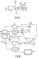
- FIG. 8 shows diagrammatically an embodiment of the measurement device in accordance with the invention in which the sampling method is used.
- FIGS 9a, 9b and 9c illustrate the principle of the novel method on the basis of the signals used.
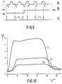
- Figure 10 shows some calibrated amplitude measurements.
- the electro-optic measurement device 1 which is the subject of the present invention and whose circuit diagram is shown in Figure 1 comprises a sensor in the form of an electro-optic crystal 3.
- the birefringence of such a crystal is changed by application of an electric field across the crystal.
- the crystal 3 is positioned as near as possible to an object to be investigated or measured.
- This object may be a semiconductor circuit (IC) 5 comprising a number of electrical conductors 7 or a printed circuit board (PCB).
- IC semiconductor circuit
- PCB printed circuit board
- the electric signal propagating through a conductor or a track then generates a local electric field which traverses the crystal and hence changes the birefringence.
- the signal can subsequently be measured on the basis of the change of the refractive index which is linearly dependent on the value of the electric signal.
- the change of the birefringence can be measured by determination of the change of phase of an optical radiation beam applied through the crystal.
- This radiation beam originated from a radiation source 9, may be, for example a linearly polarized beam.
- Said phase change can be measured in various ways.
- a first approach utilizes the fact that two propagation modes occur in the crystal and that a phase difference exists between two beam components propagating according to said modes.
- a second possibility consists in the determination of the phase difference between a measurement beam propagating according to one of the modes and a reference beam propagating outside the crystal.
- the diverging beam supplied by the radiation source 9 is converted into a parallel beam by a collimator lens 60.
- This beam is incident on a polarizer 61 which transmits a linearly polarized beam component 11 whose polarization direction encloses an angle of 45° relative to the main axis of the electro-optic crystal 3 arranged in an electric field.
- the polarization direction of the beam 11 is denoted by the arrow 11' and the direction of the main axis is denoted by the reference 6'.
- a ⁇ /2 plate 10 In the path of the beam 11 there may optionally be arranged a ⁇ /2 plate 10, where ⁇ is the wavelength of the radiation, in order to adapt the polarization direction of the beam 11 to the crystal.
- the beam 11 subsequently reaches, via a polarization-neutral beam splitter 21, a mirror 12 and subsequently an objective system 13 which is diagrammatically represented by a single lens element.
- the system 13 focuses the beam 11 in a radiation spot 15 on the lower side 17 of the crystal 3.
- the spot 15 has a diameter of from 1 to 2 ⁇ m. Due to the difference between the refractive index of the crystal 3 and that of the ambient air, the beam 11 is at least partly reflected at that area.
- the reflection can be intensified by providing a reflective layer 17' on the surface 17, for example as already described in the cited publication.
- the reflected beam 19 again traverses the crystal 3 and the object system 13, is reflected again by the mirror 12, and is subsequently transmitted by the beam splitter 21 (for example, a semitransparent mirror) to a radiation-sensitive detection system 23.
- the measurement device 1 may be connected to a visual observation system 2.
- the light beam 2 a originating from a source of visible radiation 65 and necessary for illumination of the component 5, is then transmitted, via a beam separation element 21', for example again a semitransparent mirror, in the direction of the component 5.
- the mirror 12 should then be replaced by a wavelength-selective element so that the light beam 2 a is transmitted to the component 5 and after reflection back to the observation system 2, the beam 19 reflected in the electro-optic crystal 3 being propagated substantially completely in the direction of the detector 23.
- the objective system 13 images the source 65 in a radiation spot at the area of the measurement point of the laser radiation. This point and its surroundings can be inspected by an observer by means of an eyepiece 67.
- the detection system 23 may be formed by a ⁇ /4 plate 14, succeeded by a Wollaston prism 16, two radiation sensitive detectors 18 a , 18 b , and a differential amplifier 30 as shown in Figure 2a.
- the C-axis of the ⁇ /4 plate 14 preferably extends parallel to the main axis of the crystal 3, so that the phase difference between the two components is increased by a constant factor ⁇ /2. It is thus achieved that the zero point of the measurement is shifted along the curve representing the intensity difference as a function of the phase difference, so that this point is situated halfway a slope of maximum steepness. As a result, a small phase difference results in a comparatively large difference in intensity on the detectors so that the sensitivity of the device is maximum.
- the Wollaston prism 16 splits the beam into two sub-beams 19 a , 19 b having mutually perpendicular polarization directions, the intensity distribution between the sub-beams being determined by the polarization condition of the beam 19'.
- the sub-beams 19 a and 19 b are intercepted by separate detectors 18 a and 18 b .
- the output signals S a and S b thereof, being proportional to the intensity of the sub-beam 19 a and the sub-beam 19 b , respectively, are applied to the inputs of a differential amplifier 30, the output signal S 30 of which is proportional to the signal to be measured on one of the conductors 7 of the component 5.
- the output signal S 30 is zero if the conductor does not carry a signal.
- the ⁇ /4 plate 14 in the detection chain may also be replaced by a ⁇ /4 plate 62 between the polarizer 61 and the beam splitter 21.
- the Wollaston prism 16 is preferably rotated, together with the detectors 18 a and 18 b , relative to the position occupied in the original arrangement of Figure 1.
- the component 5 to be examined and the crystal 3 are moved relative to one another, for which purpose the component 5 may be arranged, for example on a table which is movable in two directions, measurements can be performed at any desired point of the component 5 and the local behaviour of and defects in the component 5 can be detected.
- FIG. 2b shows an alternative embodiment of the detection system 23.
- the Wollaston prism 16 has been replaced by a polarization-sensitive beam splitter 20 which splits the beam to be analyzed into two sub-beams, each of which is intercepted by a detector 22 a , 22 b .
- the signals of these detectors are again applied to a differential amplifier 30.
- the detection system 23 may also include a compensator 40 denoted by a dotted line (in Figure 2a) in order to compensate for the intrinsic birefringence of the electro-optic crystal i.e. the birefringence exhibited by the crystal in the absence of an electric field.
- a compensator 40 being used if the crystal is, for example a LiTaO3 crystal, may consist of a birefringent element which introduces a phase difference between the components of the beam 19 which is equal but opposite to the phase difference caused by the intrinsic birefringence of the crystal.
- the extent of the birefringence induced in the electro-optic crystal is determined to a substantial degree by the choice of the crystal material.
- two kinds of electro-optic crystals can be used for the measurements discussed herein, i.e. crystals having a so-called longitudinal geometry and crystals having a so-called transverse geometry.
- crystals having a longitudinal geometry exclusively the electric field component which is parallel to the propagation direction of the light beam 11 entering the crystal 3 influences the optical properties of the crystal 3.
- an electro-optic material should be chosen which becomes a birefringent crystal upon application of an electric field, said crystal having a optical axis which does not extend parallel to the light beam.
- This condition limits the number of feasible crystals of longitudinal geometry.
- Materials exhibiting a cubic symmetry for example GaAs and Bi12SiO20 (BSO), are particularly suitable in this respect.
- BSO Bi12SiO20
- such cubic materials offer the advantage that no intrinsic birefringence occurs and hence no variation thereof can occur in response to a temperature variation. Consequently, no correction for these phenomena is necessary and a compensator 40 can be dispensed with in the detection system 23.
- crystals having transverse geometry In a crystal having transverse geometry, the component of the electric field which extends perpendicularly to the light beam 11 has an effect.
- the optical axis of the crystal 3 should then be situated in a plane perpendicular to the light beam 11.
- An example in this respect is LiTaO3.
- This material is uniaxial in the absence of an electric field and the optical properties are determined mainly by the component of the electric field along the optical axis.
- crystals having a longitudinal geometry are to be preferred. This is because in the case of transverse geometry the problem of cross-talk between neighbouring tracks 7 is more pronounced. In the case of longitudinal geometry, however, mainly the field above the relevant track is measured, so that the risk of cross-talk is small.
- a laser For the radiation source 9 use can be made of a laser as has already been stated.
- a semiconductor laser offering the advantage that it is compact, as is also known from the cited publication by S. Aoshima et al..
- An alternative consists in the use of a gas laser, a liquid laser or a solid state laser.
- the wavelength of the laser used is codetermined by the wavelength transmission range of the electro-optic crystal 3 used.
- FIGS. 3a and 3b show two embodiments of the measurement probe.
- a transparent, electrically conductive layer 27 may be provided on the upper side 25 of the electro-optic crystal 3.
- the layer 27 is connected to an electrically conductive layer 27' on the circumference of the carrier means 29.
- This layer 27, acting as an electrode may be made of, for example indium tin oxide and be provided on the lower portion of a radiation-transparent carrier means 29 by sputtering.
- the electrode 27' carries a reference voltage V ref .
- the reference voltage may be zero, which means that the electrode is grounded.
- the electric field across the crystal 3 is then determined by the electric field generated by the signal to be measured.
- the electrode 27' may alternatively be connected to a voltage source 31, so that the signal to be detected is measured relative to a fixed reference voltage.
- Figure 3b shows an embodiment of the measurement probe without radiation-transparent electrode 27.
- the circumferential electrode 27' it is alternatively possible to use only the circumferential electrode 27' to achieve that the potential across the upper side 25 of the electro-optic crystal 3 is sufficiently defined by the reference voltage V ref , certainly so if the electrode 27' also extends across a portion of the circumference of the crystal as shown in Figure 3b.
- the voltage source 31 is preferably adjustable as diagrammatically denoted by the arrow 32.
- the reference voltage can be adjusted on the basis of the detector signal measured; in other words, feedback control can be applied.
- V ref,c can be applied to the electrode 27 that the signal S30 ( Figure 2) equals zero.
- the value of V ref,c can be determined as diagrammatically denoted by the meter 28 and is a measure of the value of the signal to be measured.
- the resolution of the measurement device 1 is restricted not only by the optical resolution but also by the expanse of the electric field generated by a signal in a conductor 7.
- the birefringence of the crystal 3 can be influenced not only by the electric field of the signal at the point being measured at a given instant, but also by electric fields of signals in neighbouring conductors or points, in other words cross-talk between the signals may occur. This effect is even stronger when the surface of the component 5 is irregular, so that the distance between the lower side of the crystal and the component to be examined varies.
- an electrically conductive tip-shaped element which is denoted by the reference 37 in the Figures 3a and 3b.
- the voltage across the lower side 17 of the crystal 3 is determined directly, and hence in intensified and predominant manner, by the signal in the relevant conductor 7, so that the effect of signals in neighbouring conductors is strongly reduced.
- the signal S30 measured is then directly associated with the signal to be measured, so that calibration is not necessary.
- the tip-shaped element may consist of various conductive materials such as doped silicon, tungsten or a metal.
- tungsten resides in its high mechanical strength. Because tungsten is not reflective, a reflective layer should be provided on the lower side of the crystal 3 when a tungsten tip is used.
- a major advantage of a metal tip 37 consists in that the tip itself is reflective, so that it is not necessary to provide a reflective layer 17' on the lower side 17 of the crystal 3. Moreover, because only the metal tip 37 is reflective, the effective size of the radiation spot wherefrom the beam 19 originates is then determined by the diameter of the base of the metal tip 37 which is, for example, 2 ⁇ m, so that in principle less severe requirements need be imposed on the optical imaging system.
- the radiation spot 15 is made as small as possible.
- the beam 11 can be focused so as to form a small, preferably diffraction-limited radiation spot having a diameter in the order of magnitude of 1 ⁇ m by means of a suitable objective system 13
- additional refraction occurs at the carrier entrance face when use is made of a conventional carrier means 29 ( Figure 1), which refraction leads to aberrations in the measurement beam 11 and to an enlarged radiation spot 15.
- this enlargement of the spot is prevented by imparting a special shape to the carrier means 29 as shown in Figure 3a.
- the carrier means 29 is shaped as a sector of sphere whose centre of curvature coincides with the point on the lower side 17 of the crystal 3 where the main ray of the measurement beam 11 strikes the lower side 17. As a result of this shape it is achieved that all rays of the beam 11 traverse the entrance face 36 of the carrier means 29 without retraction, the reflection from this face being minimized.
- the refractive indices of the holder material, for example glass, of the electrode 27 and of the electro-optic crystal 3 it can be assured that as few as possible reflections occur at the interfaces between these three elements.
- the carrier means 29 in the form of a sector of sphere may be mounted on the objective system 13.
- Figure 3a shows a second embodiment of a special radiation-conductive carrier means 29 for the electro-optic crystal 3 which enables a radiation spot 15 of minimum dimensions to be obtained and which also protects the measurement radiation against ambient influences.
- This means 29 is formed by an optical fibre having a core 32 and a conically tapered sheath 32', radiation from a radiation source (not shown) being applied to said fibre 29 in known manner via a couple-in optical system (not shown either).
- a polarization-sustaining fibre in order to prevent influencing of the polarization condition of the radiation propagating in the fibre 29.
- the beam 11 emanating from the fibre 29 is concentrated onto the tip 37 due to total reflections at the transitions between the electro-optic material and the surrounding medium, for example air. If necessary, the fibre 29 is fully or partly covered by a metal layer 35 which is consecutive with an electrode 27 and whereto a reference voltage can be applied.
- the carrier means 29 in the form of a sector of sphere as shown in Figure 3a as well as the end of the fibre shown in Figure 3c may be mounted in an X, Y, Z manipulator 59 as shown by way of example for the carrier means 29 in Figure 4. This manipulator enables fine adjustment of the sensor in said three directions.
- FIG. 5 shows a first embodiment of the device 1 in which this possibility is used.
- the beam b supplied by a laser source 9 is split into a measurement beam b m and a reference beam b r by a beam splitter 12.
- the measurement beam b m is focused onto the lower side 17 of the electro-optic crystal 3 via a mirror 21 and the objective 13.
- the reflected measurement beam follows the same path in the reverse direction and a part of the measurement beam reaches, via the beam splitter 12, the detector 23 on which it is focused by a lens 63.
- the reference beam b r transmitted by the beam splitter 12 is incident on a reflector 41 which is constructed, for example as a cat's eye formed by a lens 42 and a mirror 49 arranged in the point of focus thereof.
- the beam reflected by the mirror 49 is combined with the reflected measurement beam by the beam splitter 12 and is applied, together therewith, to the detector 23 where the measurement beam and the reference beam interfere. It can be ensured that, in the absence of an electric field across the electro-optic crystal, the optical path length, i.e.
- the product of the geometric path length and the refractive index of the medium being traversed, of the measurement beam and the reference beam deviate by ⁇ /4 + n. ⁇ /2, where n is an integer, so that the phase difference between the two beams equals ⁇ /2 rad.
- the sensitivity of the measurement device is then maximum.
- the phase of the measurement beam is shifted with respect to that of the reference beam and the radiation intensity on the detector 23 changes due to interference of the two beams.
- the principle of the device 1 shown in Figure 5 is preferably realized by means of optical fibres as shown in Figure 6.
- the measurement beam b m is conducted by the carrier means 29, in this case a measurement fibre, and the reference beam b r is conducted by a reference fibre 31.
- the lenses 45 and 46 ensure that as much radiation as possible is coupled into the fibres 29 and 31, respectively. Because the measurement beam and the reference beam are coupled into the fibres 29, 31, they are substantially not influenced by the surroundings.
- the use of fibres also offers the advantage that a high degree of freedom is achieved in designing the measurement device.
- a measurement device of the described kind can be used, for example for testing whether or not a transistor or a integrated circuit or a PCB exhibits the desired behaviour. Furthermore, such a device can be used to trace undesirable delays in circuit and to analyse the behaviour of a signal traversing a circuit.
- a so-called dynamic detection method is used. This means that an additional modulation which is independent of the signal to be measured is imparted to the measurement signal.
- Such a dynamic detection offers the advantage that the measurement result is not influenced, or influenced to a substantially lesser extent, by, for example, drift in the electronic processing circuit, laser drift or changes in the properties of the optical components due to, for example temperature variations.
- the dynamic detection can be realized in various ways, for example by modulation of the test signal which is applied to the component to be measured and by synchronous detection of the detector signal and the test signal.
- dynamic detection can be achieved by modulation of the polarization condition of the beam entering the crystal.
- This can be achieved by means of a rotating ⁇ /2 plate arranged in the path of this beam as denoted by the arrow 47.
- Continuous rotation of the plate 14' periodically rotates the polarization direction of the beam emerging from the plate at a fixed frequency, i.e. twice the frequency of rotation of the plate.
- the intensity distribution between the sub-beams 19 a and 19 b thus varies periodically and hence also the signal S30 from the differential amplifier 30.
- the rotating ⁇ /2 plate may be arranged merely in the path of the beam 11 ( Figure 1).
- this plate 63 is arranged in the position of the previously mentioned ⁇ /2 plate 10 used to match the polarization direction of the beam 11 to the crystal 3.
- the polarization direction of the detected measurement beam is then rotated at four times the angular frequency of the plate 63.
- the direction of rotation is denoted by the arrow 64.
- the polarization direction of the beam 11 can be adapted to the crystal by adjustment of the zero position of the plate 63, so that this plate can also perform the function of the plate 10.
- the detector signal S30 is applied to a synchronous detection circuit 43 which also receives the signal S45 from a position detection system 45 and in which the signal S30 is demodulated by means of the signal S45, thus forming a signal S30, whose value is determined exclusively by the signal at the measurement point of the object.
- the position detection system 45 supplies a periodic signal having a frequency equal to twice the frequency of rotation of the plate 14 and may be derived from the control signal whereby the motor (not shown) for rotating the plate 14 is driven.
- the position detection system 45 may be constructed, for example as shown in Figure 7 and comprises an auxiliary radiation source 50 which supplies an auxiliary beam 51, a polarizer 52 which transmits a linearly polarized component of the beam emitted by the source, and an auxiliary detector 53 which is preferably a photo diode.
- the beam 51 may also be derived from the radiation source 9 ( Figure 1). Upon rotation of the ⁇ /2 plate, the detector supplies a periodic, sinusoidal signal S45.
- an optical position detection system use can alternatively be made of an inductive or capacitive position detection system.
- the radiation source 9 can be pulsed for this purpose, the duration of the pulses being substantially shorter than the period of the test signal, the starting instants of the successive pulses exhibiting an increasing delay relative to the associated period of the test signal.
- the temporal resolution is then determined by the pulse duration, provided that the latter is greater than the response time of the electro-optic crystal.
- the pulse duration may be in the order of magnitude of tens of picoseconds.
- a novel sampling method is provided which can be referred to as time delay modulation.
- FIG 8 shows diagrammatically an embodiment of a device in accordance with the invention in which the time delay modulation method can be used, and the Figures 9a, 9b and 9c illustrate the principle of the novel method on the basis of the signals used.
- the device comprises a drive circuit DC which supplies an input or test signal SI, for example a squarewave signal having a frequency of 10 MHz, for the electronic component 5 to be measured.
- the circuit DC also applies trigger pulses TP to a programmable delay generator DG.
- This generator is followed by a delay modulator DM which operates at a fixed frequency f1 in the range of, for example from 2 to 20 kHz of a frequency generator FG.
- the modulation signal MS for the delay modulator is shown in Figure 9b, and Figure 9a shows the input signal SI.
- the delay generator DG comprises a first output and a second output which supply delayed and non-delayed trigger pulses TP d and TP n , respectively.
- the delay modulator DM conducts non-delayed pulses at the instants T0 during a first half period MS1 of the modulation signal MS, and conducts delayed pulses during the second half period MS2. It is to be noted that Figure 9b shows only a small part of one period of the modulation signal MS.
- the radiation source 9 may be a diode laser which can be controlled by an external signal having a frequency of, for example 10 MHz, via a laser drive LD which is connected to the output of the delay modulator DM. Per period of the signal SI the diode laser then supplies one laser pulse LP (see Figure 9c), the laser pulses LP appearing at fixed instants T0 during the first half period of the modulation signal MS; during the second half period of the signal MS they appear at instants T1 which are adjustable via the delay generator DG.
- the laser pulses traverse the electro-optic measurement device which is diagrammatically represented by the block 80 in Figure 8 and a detailed embodiment of which is shown in Figure 1.
- the output signal of the detection system is applied to a so-called lock-in amplifier AM; when two detectors 18 a and 18 b are used, a lock-in amplifier is used which comprises a differential input whereto the modulation signal MS is also applied and whose output is connected to the input of a circuit I-M.
- the detected signal is integrated in this circuit.
- the output signal of the circuit I-M is fed back to the electrode 27 so as to be used as a reference voltage.
- the signal is also modulated, using the modulation frequency of the signal MS, between a zero level and the measured level.
- the output signal of the differential amplifier equals zero and the output signal of the integrator is constant.
- the output voltage of the integrator is then a measure of the signal SI at the instants T1 if the signal SI is zero at the instants T0. If the signal SI has a different value at the instants T0, the zero level of the integrator output signal is shifted. The amplitude of this signal is still calibrated, because a zero point method is used.
- the measurement of the signal at the instant T1 is performed a large number of times because of the large number of laser pulses within the half period SM2 of the modulation signal MS.
- This number of pulses amounts to, for example, one thousand when the frequency of the signal SI is 10 MHz and that of the modulation signal MS is 10 kHz.
- a reliable measurement signal is obtained at the instant T1 when an average is taken over such a large number of measurements.
- This measurement signal is compared with the mean signal of an equally large number of measurements at the instants T0.
- the delay of the generator DG is slightly changed, for example in the order of magnitude of two hundred picoseconds, and a second mean measurement is executed at a second instant T1.
- the laser pulses PL having a brief duration of, for example, fifty picoseconds, one period of the periodic signal at a measurement point of the electronic component 5 can be sampled.
- Figure 10 shows the result of such a measurement for a track having a width of 8 ⁇ m.
- the delay T d is plotted in nanoseconds in the horizontal direction and the measured signal S30 is plotted in the vertical direction.
- the curves C1, C2 and C3, are associated with amplitudes of the output signal SI amounting to 5V, 2V and 1V, respectively, the repetition frequency of the laser pulse being 10 MHz.
- the device shown in Figure 8 also comprises a computer CO for programming the delay T d of the generator DG, for measuring and storing the output signal of the integrator, and for controlling a display device MO for the waveform.
- the voltage across the electrode 27 is modulated in synchronism with the time delay modulation. This also holds if the input signal SI is modulated.
- the time delay modulation method described with reference to the Figures 8, 9 and 10 for an electro-optic measurement device can also be used in, for example a measurement device in which the measurement beam is a charged particle beam such as an ion beam or an electron beam.
- a measurement device utilizing an electron beam is disclosed in the article "Integrated Circuit Diagnostic Tools", Philips J. Res. 41 (1989), pages 295-327, notably section 2.3, pages 303-308.
- the diagram of the measurement device utilizing an electron beam in conjunction with the time delay modulation method in accordance with the invention is analogous to that of Figure 8, be it that the block 80 and the component 5 are replaced by the arrangement shown in Figure 6 of the cited article.
Landscapes
- Physics & Mathematics (AREA)
- Engineering & Computer Science (AREA)
- General Physics & Mathematics (AREA)
- Health & Medical Sciences (AREA)
- Computer Vision & Pattern Recognition (AREA)
- Electromagnetism (AREA)
- Toxicology (AREA)
- General Engineering & Computer Science (AREA)
- Tests Of Electronic Circuits (AREA)
- Measuring Instrument Details And Bridges, And Automatic Balancing Devices (AREA)
- Measurement Of Current Or Voltage (AREA)
Applications Claiming Priority (2)
| Application Number | Priority Date | Filing Date | Title |
|---|---|---|---|
| EP91202003 | 1991-08-05 | ||
| EP91202003 | 1991-08-05 |
Publications (3)
| Publication Number | Publication Date |
|---|---|
| EP0541139A2 true EP0541139A2 (fr) | 1993-05-12 |
| EP0541139A3 EP0541139A3 (en) | 1993-06-09 |
| EP0541139B1 EP0541139B1 (fr) | 2003-01-22 |
Family
ID=8207815
Family Applications (1)
| Application Number | Title | Priority Date | Filing Date |
|---|---|---|---|
| EP92202279A Expired - Lifetime EP0541139B1 (fr) | 1991-08-05 | 1992-07-24 | Dispositif de mesure électro-optique pour la mesure d'un signal électrique dans un composant électronique |
Country Status (4)
| Country | Link |
|---|---|
| US (1) | US5459394A (fr) |
| EP (1) | EP0541139B1 (fr) |
| JP (1) | JP3278460B2 (fr) |
| DE (1) | DE69232905T2 (fr) |
Cited By (7)
| Publication number | Priority date | Publication date | Assignee | Title |
|---|---|---|---|---|
| EP0587418A3 (fr) * | 1992-09-10 | 1995-02-01 | Hamamatsu Photonics Kk | Sonde électro-optique. |
| EP0581556A3 (fr) * | 1992-07-28 | 1995-02-08 | Hewlett Packard Co | Sonde de test sans contact et appareil de mesure de tension du type sans contact. |
| EP0645635A3 (fr) * | 1993-09-28 | 1995-06-14 | Hamamatsu Photonics Kk | Détecteur électro-optique de tension. |
| EP0663596A3 (fr) * | 1994-01-12 | 1996-08-07 | Hamamatsu Photonics Kk | Sonde électro-optique de potentiel avec une plaque de fibres optiques. |
| EP0806678A3 (fr) * | 1996-05-10 | 1997-11-26 | Schlumberger Technologies, Inc. | Sonde de potentiel à laser |
| EP0864872A3 (fr) * | 1997-03-15 | 1999-03-17 | Schlumberger Technologies, Inc. | Sondage de tension de circuits intégrés par double laser |
| WO2016177493A1 (fr) * | 2015-05-07 | 2016-11-10 | Asml Netherlands B.V. | Appareil et procédé de mesure |
Families Citing this family (10)
| Publication number | Priority date | Publication date | Assignee | Title |
|---|---|---|---|---|
| US6414473B1 (en) * | 1996-05-31 | 2002-07-02 | Rensselaer Polytechnic Institute | Electro-optic/magneto-optic measurement of electromagnetic radiation using chirped optical pulse |
| US6144004A (en) * | 1998-10-30 | 2000-11-07 | Magnetic Separation Systems, Inc. | Optical glass sorting machine and method |
| JP2000221213A (ja) * | 1998-11-24 | 2000-08-11 | Ando Electric Co Ltd | 電気光学プロ―ブ |
| WO2001094955A2 (fr) * | 2000-06-09 | 2001-12-13 | The Regents Of The University Of Michigan | Imageur de champs electromagnetiques a balayage pourvu d'un systeme a base de fibre optique pour la cartographie des champs electro-optiques |
| US6894514B2 (en) * | 2000-12-01 | 2005-05-17 | Toppan Printing Co., Ltd. | Circuit pattern detecting apparatus and circuit pattern inspecting method |
| US6906506B1 (en) | 2001-06-08 | 2005-06-14 | The Regents Of The University Of Michigan | Method and apparatus for simultaneous measurement of electric field and temperature using an electrooptic semiconductor probe |
| JP6711983B2 (ja) * | 2015-11-29 | 2020-06-17 | 山梨県 | 光電界センサおよび電磁界計測装置 |
| CN110383086B (zh) * | 2017-03-06 | 2021-08-24 | 国立大学法人大阪大学 | 电磁波测量装置以及电磁波测量方法 |
| US11079432B2 (en) * | 2019-02-19 | 2021-08-03 | Nxp B.V. | Integrated laser voltage probe pad for measuring DC or low frequency AC electrical parameters with laser based optical probing techniques |
| JP7271283B2 (ja) * | 2019-04-16 | 2023-05-11 | 株式会社日本マイクロニクス | 検査用接続装置 |
Family Cites Families (10)
| Publication number | Priority date | Publication date | Assignee | Title |
|---|---|---|---|---|
| DE2813947C2 (de) * | 1978-03-31 | 1986-09-04 | Siemens AG, 1000 Berlin und 8000 München | Verfahren zur berührungslosen Messung des Potentialverlaufs in einem elektronischen Bauelement und Anordnung zur Durchführung des Verfahrens |
| DE3235484A1 (de) * | 1982-09-24 | 1984-03-29 | Siemens AG, 1000 Berlin und 8000 München | Verfahren zur unterdrueckung einer stoerung bei der messung von signalverlaeufen mit einer korpuskularsonde und vorrichtung zur durchfuehrung eines solchen verfahrens |
| JP2571385B2 (ja) * | 1987-05-31 | 1997-01-16 | 浜松ホトニクス株式会社 | 電圧検出装置 |
| US4996475A (en) * | 1987-05-31 | 1991-02-26 | Hamamatsu Photonics Kabushiki Kaisha | Electro-optic voltage detector having a transparent electrode |
| US4857836A (en) * | 1987-06-09 | 1989-08-15 | Siemens Aktiengesellschaft | Mechanical probe for optical measurement of electrical signals |
| FR2633055B2 (fr) * | 1987-07-31 | 1991-01-04 | Schlumberger Ind Sa | Perfectionnements aux testeurs de circuits |
| DE3889986T2 (de) * | 1987-07-13 | 1994-09-15 | Hamamatsu Photonics Kk | Anordnung eines Spannungsdetektors. |
| US5041783A (en) * | 1989-02-13 | 1991-08-20 | Olympus Optical Co., Ltd. | Probe unit for an atomic probe microscope |
| DE69010053T2 (de) * | 1989-04-12 | 1994-10-13 | Hamamatsu Photonics Kk | Methode und Vorrichtung zum Nachweis einer Spannung. |
| US5006789A (en) * | 1989-05-23 | 1991-04-09 | The University Of Rochester | Electro-optic signal measurement |
-
1992
- 1992-07-24 EP EP92202279A patent/EP0541139B1/fr not_active Expired - Lifetime
- 1992-07-24 DE DE69232905T patent/DE69232905T2/de not_active Expired - Fee Related
- 1992-08-04 JP JP20810392A patent/JP3278460B2/ja not_active Expired - Fee Related
-
1993
- 1993-08-27 US US08/113,535 patent/US5459394A/en not_active Expired - Fee Related
Cited By (12)
| Publication number | Priority date | Publication date | Assignee | Title |
|---|---|---|---|---|
| EP0581556A3 (fr) * | 1992-07-28 | 1995-02-08 | Hewlett Packard Co | Sonde de test sans contact et appareil de mesure de tension du type sans contact. |
| US5465043A (en) * | 1992-07-28 | 1995-11-07 | Hewlett-Packard Company | Non-contact type probe and non-contact type voltage measuring apparatus, wherein the probe's irradiation surface is coated with a conductive film having a pinhole |
| EP0587418A3 (fr) * | 1992-09-10 | 1995-02-01 | Hamamatsu Photonics Kk | Sonde électro-optique. |
| US5500587A (en) * | 1992-09-10 | 1996-03-19 | Hamamatsu Photonics K.K. | E-O probe |
| EP0645635A3 (fr) * | 1993-09-28 | 1995-06-14 | Hamamatsu Photonics Kk | Détecteur électro-optique de tension. |
| US5479106A (en) * | 1993-09-28 | 1995-12-26 | Hamamatsu Photonics K.K. | Electro-optic voltage detector |
| EP0663596A3 (fr) * | 1994-01-12 | 1996-08-07 | Hamamatsu Photonics Kk | Sonde électro-optique de potentiel avec une plaque de fibres optiques. |
| US5585735A (en) * | 1994-01-12 | 1996-12-17 | Hamamatsu Photonics K.K. | E-O probe with FOP and voltage detecting apparatus using the E-O probe |
| EP0806678A3 (fr) * | 1996-05-10 | 1997-11-26 | Schlumberger Technologies, Inc. | Sonde de potentiel à laser |
| EP0864872A3 (fr) * | 1997-03-15 | 1999-03-17 | Schlumberger Technologies, Inc. | Sondage de tension de circuits intégrés par double laser |
| WO2016177493A1 (fr) * | 2015-05-07 | 2016-11-10 | Asml Netherlands B.V. | Appareil et procédé de mesure |
| US10185230B2 (en) | 2015-05-07 | 2019-01-22 | Asml Netherlands B.V. | Measurement apparatus and method |
Also Published As
| Publication number | Publication date |
|---|---|
| EP0541139A3 (en) | 1993-06-09 |
| EP0541139B1 (fr) | 2003-01-22 |
| DE69232905T2 (de) | 2003-08-21 |
| US5459394A (en) | 1995-10-17 |
| DE69232905D1 (de) | 2003-02-27 |
| JP3278460B2 (ja) | 2002-04-30 |
| JPH05249201A (ja) | 1993-09-28 |
Similar Documents
| Publication | Publication Date | Title |
|---|---|---|
| US5459394A (en) | Electro-optic measurement device for the measurement of an electric signal in an electronic component | |
| US7898668B2 (en) | Terahertz spectrometer | |
| US5999005A (en) | Voltage and displacement measuring apparatus and probe | |
| KR100262878B1 (ko) | 근접시야 광학현미경 및 그 측정방법 | |
| GB2369432A (en) | Electro-optic probe and magneto-optic probe | |
| US4891580A (en) | Electro-optic measurements of voltage waveforms on electrical conductors | |
| JPH0573178B2 (fr) | ||
| JP2001159665A (ja) | 集積回路デバイスの波形による精査のための二パルス利用型光干渉計 | |
| US4999570A (en) | Device for making non-contacting measurements of electric fields which are statical and/or varying in time | |
| JPS63313075A (ja) | 電位を光学的に測定するための機械式プローブ | |
| US4982151A (en) | Voltage measuring apparatus | |
| US5583446A (en) | Electro-optically controlled measurement probe system | |
| US4873485A (en) | Electro-optic signal measurement | |
| JPH0695111B2 (ja) | 電圧検出装置 | |
| Robinson et al. | The measurement of the frequency response of a photodiode and amplifier using an opto-mechanical frequency response calibrator | |
| JP2947288B2 (ja) | 半導体集積回路用試験装置および該装置のプローブ位置制御方法 | |
| JPH0580083A (ja) | 集積回路の試験方法および装置 | |
| US6469528B2 (en) | Electro-optic sampling probe and measuring method using the same | |
| US6297651B1 (en) | Electro-optic sampling probe having unit for adjusting quantity of light incident on electro-optic sampling optical system module | |
| GB2346692A (en) | Electro-optic probe | |
| JPH0695108B2 (ja) | 回路電圧検出装置 | |
| JPH0787211B2 (ja) | 集積回路の試験装置 | |
| JP3018982B2 (ja) | プリント基板の信号波形測定装置 | |
| KR920000565B1 (ko) | 전도체 전기 신호의 전압 파형 측정 방법 및 그 장치 | |
| GB2348283A (en) | Electro-optic probe |
Legal Events
| Date | Code | Title | Description |
|---|---|---|---|
| AK | Designated contracting states |
Kind code of ref document: A2 Designated state(s): DE FR GB |
|
| PUAI | Public reference made under article 153(3) epc to a published international application that has entered the european phase |
Free format text: ORIGINAL CODE: 0009012 |
|
| PUAL | Search report despatched |
Free format text: ORIGINAL CODE: 0009013 |
|
| D17D | Deferred search report published (deleted) | ||
| D17D | Deferred search report published (deleted) | ||
| DA1 | Application published (deleted) | ||
| AK | Designated contracting states |
Kind code of ref document: A2 Designated state(s): DE FR GB |
|
| AK | Designated contracting states |
Kind code of ref document: A3 Designated state(s): DE FR GB |
|
| 17P | Request for examination filed |
Effective date: 19931125 |
|
| 17Q | First examination report despatched |
Effective date: 19960403 |
|
| RAP3 | Party data changed (applicant data changed or rights of an application transferred) |
Owner name: KONINKLIJKE PHILIPS ELECTRONICS N.V. |
|
| GRAG | Despatch of communication of intention to grant |
Free format text: ORIGINAL CODE: EPIDOS AGRA |
|
| RIC1 | Information provided on ipc code assigned before grant |
Free format text: 7G 01R 31/308 A, 7G 01R 1/067 B |
|
| RTI1 | Title (correction) |
Free format text: ELECTRO-OPTIC MEASUREMENT DEVICE FOR THE MEASUREMENT OF AN ELECTRICAL SIGNAL IN AN ELECTRONIC COMPONENT |
|
| RIC1 | Information provided on ipc code assigned before grant |
Free format text: 7G 01R 31/308 A, 7G 01R 1/067 B |
|
| RTI1 | Title (correction) |
Free format text: ELECTRO-OPTIC MEASUREMENT DEVICE FOR THE MEASUREMENT OF AN ELECTRICAL SIGNAL IN AN ELECTRONIC COMPONENT |
|
| GRAG | Despatch of communication of intention to grant |
Free format text: ORIGINAL CODE: EPIDOS AGRA |
|
| GRAH | Despatch of communication of intention to grant a patent |
Free format text: ORIGINAL CODE: EPIDOS IGRA |
|
| GRAH | Despatch of communication of intention to grant a patent |
Free format text: ORIGINAL CODE: EPIDOS IGRA |
|
| GRAA | (expected) grant |
Free format text: ORIGINAL CODE: 0009210 |
|
| XX | Miscellaneous (additional remarks) |
Free format text: DIE ANMELDUNG IST BEREITS AM 24.02.93 UNTER EINER ANDEREN PUBLIKATIONSNUMMER VOM EPA ZUM ERSTEN MAL VEROEFFENTLICHT WORDEN. |
|
| AK | Designated contracting states |
Kind code of ref document: B1 Designated state(s): DE FR GB |
|
| REG | Reference to a national code |
Ref country code: GB Ref legal event code: FG4D |
|
| XX | Miscellaneous (additional remarks) |
Free format text: DIE ANMELDUNG IST BEREITS AM 24.02.93 UNTER EINER ANDEREN PUBLIKATIONSNUMMER VOM EPA ZUM ERSTEN MAL VEROEFFENTLICHT WORDEN. |
|
| REF | Corresponds to: |
Ref document number: 69232905 Country of ref document: DE Date of ref document: 20030227 Kind code of ref document: P |
|
| ET | Fr: translation filed | ||
| PLBE | No opposition filed within time limit |
Free format text: ORIGINAL CODE: 0009261 |
|
| 26N | No opposition filed |
Effective date: 20031023 |
|
| PGFP | Annual fee paid to national office [announced via postgrant information from national office to epo] |
Ref country code: GB Payment date: 20050727 Year of fee payment: 14 |
|
| PGFP | Annual fee paid to national office [announced via postgrant information from national office to epo] |
Ref country code: FR Payment date: 20050729 Year of fee payment: 14 |
|
| PGFP | Annual fee paid to national office [announced via postgrant information from national office to epo] |
Ref country code: DE Payment date: 20050913 Year of fee payment: 14 |
|
| PG25 | Lapsed in a contracting state [announced via postgrant information from national office to epo] |
Ref country code: GB Free format text: LAPSE BECAUSE OF NON-PAYMENT OF DUE FEES Effective date: 20060724 |
|
| PG25 | Lapsed in a contracting state [announced via postgrant information from national office to epo] |
Ref country code: DE Free format text: LAPSE BECAUSE OF NON-PAYMENT OF DUE FEES Effective date: 20070201 |
|
| GBPC | Gb: european patent ceased through non-payment of renewal fee |
Effective date: 20060724 |
|
| REG | Reference to a national code |
Ref country code: FR Ref legal event code: ST Effective date: 20070330 |
|
| PG25 | Lapsed in a contracting state [announced via postgrant information from national office to epo] |
Ref country code: FR Free format text: LAPSE BECAUSE OF NON-PAYMENT OF DUE FEES Effective date: 20060731 |