EP0541303A2 - Optisches Kreislauf-Schieberegister - Google Patents
Optisches Kreislauf-Schieberegister Download PDFInfo
- Publication number
- EP0541303A2 EP0541303A2 EP92309952A EP92309952A EP0541303A2 EP 0541303 A2 EP0541303 A2 EP 0541303A2 EP 92309952 A EP92309952 A EP 92309952A EP 92309952 A EP92309952 A EP 92309952A EP 0541303 A2 EP0541303 A2 EP 0541303A2
- Authority
- EP
- European Patent Office
- Prior art keywords
- signal
- encoded
- control
- medium
- shift register
- Prior art date
- Legal status (The legal status is an assumption and is not a legal conclusion. Google has not performed a legal analysis and makes no representation as to the accuracy of the status listed.)
- Granted
Links
Images


Classifications
-
- G—PHYSICS
- G11—INFORMATION STORAGE
- G11C—STATIC STORES
- G11C21/00—Digital stores in which the information circulates continuously
-
- G—PHYSICS
- G02—OPTICS
- G02B—OPTICAL ELEMENTS, SYSTEMS OR APPARATUS
- G02B6/00—Light guides; Structural details of arrangements comprising light guides and other optical elements, e.g. couplings
- G02B6/24—Coupling light guides
- G02B6/26—Optical coupling means
- G02B6/28—Optical coupling means having data bus means, i.e. plural waveguides interconnected and providing an inherently bidirectional system by mixing and splitting signals
- G02B6/2804—Optical coupling means having data bus means, i.e. plural waveguides interconnected and providing an inherently bidirectional system by mixing and splitting signals forming multipart couplers without wavelength selective elements, e.g. "T" couplers, star couplers
- G02B6/2821—Optical coupling means having data bus means, i.e. plural waveguides interconnected and providing an inherently bidirectional system by mixing and splitting signals forming multipart couplers without wavelength selective elements, e.g. "T" couplers, star couplers using lateral coupling between contiguous fibres to split or combine optical signals
- G02B6/2843—Optical coupling means having data bus means, i.e. plural waveguides interconnected and providing an inherently bidirectional system by mixing and splitting signals forming multipart couplers without wavelength selective elements, e.g. "T" couplers, star couplers using lateral coupling between contiguous fibres to split or combine optical signals the couplers having polarisation maintaining or holding properties
Definitions
- This invention relates to optical digital circuits and, more particularly, to an optical circulating shift register.
- All-optical information processing holds promise for processing throughput rates which are much faster than electronics.
- silica optical fiber remains the most promising medium for realizing all-optical processing systems.
- the fiber loss is low enough that extremely long lengths can be used to compensate for the weak nonlinearity, and there is tremendous amount of existing technology that can be exploited in building a system.
- All-optical fiber Sagnac interferometer switches have been demonstrated in a number of different formats, and at extremely high speeds. Such Sagnac switches are extremely simple structures which are also immune to fluctuations in ambient conditions, and much experience has been accumulated in the development of Sagnac-based fiber optic gyroscopes.
- a control beam must be used which is isolated from a separate signal beam.
- Two distinct optical wavelengths can be used, in which case lossless combination and separation of the control and signal can be effected using wavelength dependent couplers or filters. While the use of different wavelengths is an elegant scheme for a simple system, problems develop as the system grows in complexity, as identical devices of this type cannot be cascaded with an identical device.
- a polarization-based Sagnac switch was demonstrated, in which polarization rather than wavelength was used to distinguish the control beam from the signal beam. Stable polarization-based interferometry is simply achieved in a Sagnac switch by using polarizing couplers.
- an optical circulating shift register is implemented using an optical encoding means.
- the encoding means encodes a received optical clock signal with a value derived from an encoded optical signal received at a control port.
- the resulting encoded clock signal, appearing at an output port, is then coupled, or circulated, back to the control port.
- the encoding means uses the encoded clock signal at the control port to encode a subsequently received clock signal.
- the encoding means is implemented using a Sagnac switch arrangement including an optical transmission medium having a controllable propagation speed characteristic.
- the Sagnac switch is modified to include a feedback path connected between a non-reflecting output port thereof and a control port thereof.
- An optical clock signal is received at an input port of the Sagnac switch and an encoded data signal is received at the control port.
- the Sagnac switch encodes the clock signal received at the input port with a value derived from the encoded signal received at the control port.
- the encoded clock signal at the output port is then coupled back, via the feedback path, to the control port.
- the shift register also outputs the encoded clock signal.
- the optical shift register is implemented using the Sagnac switch arrangement described above except that the feedback path connects a reflected output port of the Sagnac switch to the control port of the Sagnac switch.
- the shift register alternately outputs the encoded clock signal and the inverse of the encoded clock signal.
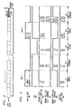
- FIG. 1 Shown in FIG. 1 is an illustrative diagram of our inventive optical circulating shift register 100 comprising an encoding means, implemented using a Sagnac interferometer switch arrangement 110 (hereinafter Sagnac switch), and a feedback path 120.
- Sagnac switch a Sagnac interferometer switch arrangement 110
- a feedback path 120 a Sagnac switch.
- Such a Sagnac switch is described in more detail in the co-pending United States patent application, Serial No. 07/521774 of Gabriel, Houh and Whitaker entitled “Sagnac Optical Logic Gate,” filed May 10, 1990, which is incorporated by reference herein.
- the Sagnac switch 110 includes an optical transmission medium, i.e., an optical fiber 10, that is connected at both ends to a Polarization Maintaining Coupler (PMC) 20.
- An input clock signal is applied to an input SI which is port 1 of the coupler 20, ports 2 and 4 of coupler 20 are connected to the two ends of fiber 10, and port 3 of coupler 20 forms an output S0 of the Sagnac loop.
- Fiber 10 thus forms a loop, (also referred to herein as fiber loop 10) which in the context of this disclosure, refers to the path over which a signal travels and, more particularly, to arrangements where the path forms a closed, or nearly closed, figure.
- the Sagnac switch 110 operates as follows.
- the clock signal may be a single pulse or a plurality of pulses.
- the data input and control signals may also be one or more pulses.
- An input clock signal applied to port 1 is split into two parts that exit coupler 20 at ports 2 and 4: a "mark” signal that travels clockwise, and a “ref” signal (reference signal) that travels counter-clockwise.
- the "mark” and “ref” signals travel through the loop in opposite directions, re-enter coupler 20 and recombine therein. Under normal circumstances, the "mark” and “ref” signals experience the same conditions as they travel through the loop.
- FIG. 1 includes a polarization combining coupler (PBS1) 30 that injects a control signal at port CTLI into a segment 11 of the fiber loop 10. Because coupler 30 is within the loop, the control signal travels along the loop only in one direction; and more specifically, coupler 30 is arranged to inject the control signal that travels along the loop in the direction of the "mark" signal.
- a polarization combining coupler (PBS2) 50 is also included within the loop of fiber 10 to extract the control pulse out of the loop once it has served its control function.
- Segment 11 of fiber 10 is a variable refractive-index material that is characterized by the property that the propagation speed of a beam passing through the material is a function of the energy of the beam that passes through the material. Furthermore, not only does the propagation speed change for the beam (e.g., control signal) that effects the change in propagation speed, but it also changes the propagation speed of other beams (e.g., "mark" signal) that pass through the material at the same time. The nonlinear interaction between the control signal and the "mark” signal is by means of cross-phase modulation due to the optical Kerr effect.
- the entire length of fiber 10 may be made of such a variable refractive-index material, but for the sake of generality, FIG.
- FIG. 1 is drawn with only a limited segment being made up of this material. Also for the sake of generality, it should be pointed out that the loop of fiber 10 in FIG. 1 does not necessarily have to be fiber. It can be a waveguide, or other means for directing the flow of light.
- the arrangement of FIG. 1 includes a fiber loop 10 having a controllable propagation speed material in segment 11, "mark” and “ref” signals traveling through the loop in opposite directions and combined in coupler 20 and a control signal that is injected at coupler 30 which travels in the same direction as the "mark” signal over segment 11 and extracted by coupler 50.
- the "mark” and control signals are properly timed and conditioned, the result is a single-pole double-throw switch type apparatus.
- the "mark” and “ref” signals are combined in coupler 20 as described above.
- the signal entering the switch at port 1 reflects out of the loop of fiber 10 and exits out of port 1 of coupler 20.
- the Sagnac switch To ensure the proper operation of the Sagnac switch (that is to minimize the distortion of the pulse which outputs at port 3) requires that the control signal completely traverse the "mark" signal during its transit through segment 11 of the fiber loop 10. This is accomplished by requiring that the material of segment 11 have a dual speed characteristic, one that propagates the control signal at a different rate than the "mark" signal. The difference in the propagation speed may be tied to any controllable parameter of the control signal, such as wavelength, intensity or polarization. As long as the control signal completely traverses the "mark” signal within segment 11 the Sagnac switch operation is completely insensitive to the shape of the control signal or its precise timing. Rather, it is only sensitive to the overall energy of the control signal (integral of the control pulse).
- segment 11 is selected to have a controllable parameter based on polarization alone or on polarization and intensity together.
- the length of segment 11 must be selected together with the controllable parameter to ensure that the control signal can traverse or "slip" past the "mark” signal within the length of segment 11, even though the "mark” signal precedes the entrance of the control signal into segment 11.
- the fiber loop 10 is formed from polarization maintaining fiber (PMF).
- a polarization maintaining coupler (PMC) is used as a coupler 20 to form the Sagnac switch.
- the clock signal is split into two equal signals (i.e., "mark” and "ref” signals) by coupler 20, which each traverse the loop in different directions and recombine interferometrically at coupler 20.
- the clock signal is held in a single linearly polarized state in fiber loop 10, and the control signal is introduced into fiber loop 10 in an orthogonal state using a polarization combining coupler (PBSI) as coupler 20.
- PBSI polarization combining coupler
- a polarization splitting coupler (PBS2) is used as coupler 50 to extract the control signal out of fiber loop 10. With ideal components this makes possible lossless combination and perfect isolation of the control and the "mark” and "ref” signals.
- segment 11 of the loop consists of an odd number of sections and an even number of crossed-axis splices.
- Segment 11 of the loop is illustratively shown as consisting of 9 sections, separated by 8 crossed-axis splices (i.e., adjacent sections are connected such that the birefringent axes are orthogonal.)
- this corresponds to a determinable amount of slip between the control signal and the "mark" signal in each section.
- These splices allow the control signal and "mark” signal to multiply interact (i.e., alternately traverse or slip by each other) and provides other benefits such as jitter independence, removal of coherence problems, and pulse shape tolerance.
- control signal CTLI When control signal CTLI is absent, the recombining "mark” and “ref” signals interfere at coupler 20 so that a combined signal is reflected back into input port 1 of the Sagnac loop 110.
- a nonlinear phase shift on the half of the clock signal (“mark” signal) with which it co-travels causes a combined signal to be transmitted to port 3 rather than reflected out at port 1.
- the transmitted or non-reflected signal SO from Sagnac switch 110 is logically equivalent to the control signal CTLI (delayed) and is amplified by an erbium-doped fiber amplifier (EDFA) 160 and fed back, via feedback path 120, to provide control signal CTLI.
- the feedback path 120 adds a small predetermined time delay to the feedback signal. While the amplifier 160 in feedback path 120 has been described as an erbium amplifier, other optical amplifiers may be utilized. Additionally, it should be noted that this amplifier may be placed in loop 10 rather than in feedback path 120.
- the erbium amplifier (EDFA) 160 is eliminated and replaced by path 170.
- EDFA erbium amplifier
- Such an embodiment is useful when 1) losses at the vinous splices are very small, 2) sufficient crossed-axis splices exist, 3) the segment 11 length is sufficiently long or 4) enhanced non-linear refractive index fiber is used. Any one or combination of these characteristics may result in an unamplified feedback control signal still having enough energy to create sufficient propagation speed changes needed to enable the control signal to give a substantially 180° phase shift to the "mark" signal.
- control signal CTLI is set at the fast transit polarization angle of loop 10.
- the length of the feedback loop 120 is selected so that the first control signal CTLI arrives at coupler 30 a predetermined period of time after the first clock signal arrives there.
- the length of segment 11 of loop 10 is such that a control signal, travelling on the fast transit polarization angle of loop 10 will completely traverse (or slip past) its associated "mark" clock signal, travelling on the slow transit polarization angle of loop 10.
- this ensures that the "mark" clock signal will traverse loop 10 faster than the "ref” clock signal so that the combining at coupler 20 is completely destructive with regard to port 1 and completely constructive with regard to port 3.
- all of the energy of the clock signal emerges at port 3.
- the combined length of loop 10 together with feedback path 120 holds a predetermined number of clock signals (e.g., a frame of clock pulses).
- a predetermined number of clock signals e.g., a frame of clock pulses.
- the transit through loop 10 and feedback path 120 takes a predetermined time interval (one frame time).
- the ratio of the length of feedback path 120 to the length of fiber loop 10 is not critical, so long as the fiber loop 10 is long enough to provide the required slip.
- the data input may be generated by using a widely available optical modulator 150 of FIG. 1 to encode the input data pattern onto an optical pulse stream from laser 190.
- This encoded pattern of optical pulses i.e., the data
- the clock signal is inputted serially into the input lead SI of the Sagnac switch 110.
- data can be entered into the shift register 100 by using several means: 1. modulating the clock signal (MOD 480 of FIG. 4); 2. coupling a separate optical signal into the feedback loop (C2 of FIG. 1); 3. modulating the signal in the feedback loop (MOD 191 of FIG. 1) ; 4. entering data via a second control port (coupler 50 of FIG. 1) of the Sagnac switch 110.
- the above configuration implements an optical equivalence of an N bit circulating shift register with an amplifier in its feedback path.
- the bit length N of the shift register is determined by both the time between input pulses and the time it takes the light pulses to traverse the entire circuit.
- the clock signal 130 is provided by the pulsed laser 140.
- the power supply is provided by the erbium amplifier 160.
- the data input is provided, illustratively, by a modulator 150 coupled to a laser source 140 and coupled via coupler C2, into the shift register 100.
- the data output is provided by a coupler C4, illustratively, connected to the feedback loop 120.
- a clear shift register function is provided, illustratively, by modulator 180 in series with the pulsed laser 140 clock source.
- a narrowband filter F is used to prevent the circulating shift register 100 from lasing through leakage around the fiber loop 10 and feedback loop 120.
- FIG. 3 illustrates two data storage operations DATA1 and DATA2.
- data storage operation one includes a data input (write) frame 311, data storage frames 312 and a data clear frame 313.
- Data storage operation two includes a data write frame 314 and data storage frames 315.
- the clock signal and data signal comprise a plurality or frame of pulses.
- the envelope of the optical pulses is illustrated for the data input (SRI) 301, clock 302, control 303, Sagnac switch input (SI) 304, Sagnac switch output (SO) 305 and shift register (SRO) output 306.
- the first frame of data inputted at data input 301 of FIG. 3, write frame 311, includes a string of pulses (a) representing logic 1 bits, followed by an absence of pulses (b) representing a string of logic 0 bits, followed by a string of pulses (c) representing logic 1 bits.
- the control input sequence at CTLI and the shift register output sequence SRO are logically equivalent to the data in sequence 301 (DATA 1) during write frame 1, 311.
- the sequence at port SO is derived from the sequence at port CTLI of the previous frame.
- the Sagnac at port SO during frame 312 is the same as the sequence at port CTLI during frame 311.
- the sequence at port SI is the logical complement of the sequence at port SO.
- the shift register output port SRO always carries the same sequence as port CTLI. This pattern continues indefinitely as long as the clock pulses are supplied. That is, in our example, the various sequences in frames 2 through X are the same.
- the clock signal 302 is interrupted for one complete frame using the clear modulation 180. This is shown in the clear frame 313.
- the output sequence SRO persists during the clear frame 313 as the Sagnac loop is emptied of light.
- the new data input sequence DATA 2 appears immediately both at the shift register output SRO and at the control port CTLI.
- the SO and SI ports have no signals during this frame as the loop is being refilled with sequence DATA 2.
- the DATA 2 sequence persists in the shift register, as shown by frame 315.
- control signal CTLI is the logical "ORing" of the data input signal and the port SO signal of Sagnac switch 110.
- the output at port SI i.e., the reflected output at SI
- the output at port SO is the logical "ANDing" of the clock pulse and the control signal CTLI.
- the output SRO of the circulating shift register 100 is the same as the control signal CTLI.
- the output coupler C4 can also be placed prior to the data in coupler C2 in feedback loop 120. In such an embodiment, the output SRO would have no "data in” signal present during the write frame 311, that is, SRO would then have the same sequence as Sagnac port SO.
- FIG. 4 Shown in FIG. 4 is a second embodiment of our invention.
- FIG. 4 is very similar to the arrangement of FIG. 3 except that the feedback loop 120 extends between coupler 1 on the input port SI and the control port CTLI of Sagnac switch 110.
- the FIG. 4 embodiment offers the advantage of having the "data in” and its inverse signal available at the output SRO during alternate frames. This embodiment also keeps the amplifier power constant.
- FIG. 5 depicts a schematic representation for the shift register embodiment illustrated in FIG. 4. This schematic is distinguished from that of FIG. 2 by the presence of a logical inverter in the feedback path.
- the inverter forms the logical complement of the data in the loop after every round trip (one frame).
- the stored data sequence at the output SRO is logically complemented in alternate frames.
- a clear operation can take place during any frame, and a write operation can take place during any frame after a clear operation.
- FIG. 6 illustrates a data write operation 611, followed by three storage frames 612-614 and a subsequent clear frame 615.
- the control input sequence at CTLI and the shift register output sequence SRO are logically equivalent to the data in sequence 601 during the first frame 611.
- the sequence at port SO is a replica of the sequence at port CTLI of frame 1, 611.
- the sequence at port SOI is the logical complement control signal at CTLI of frame 1, 611.
- the sequence leaving port SOI produces the output sequence SRO as well as the new control signal at CTLI for frame 2, 612. Note that the sequences at ports SO1, SRO and CTLI are always the same except during a write frame, 611.
- the pattern at control port CTLI becomes replicated at port SO.
- the pattern at port SOI is the logical inverse of the pattern at port SO, and provides the new control signal at port CTLI. This process is repeated for all subsequent storage frames.
- the clear frame 515 is affected by interrupting the clock signal 502 to empty the light from the Sagnac loop 10. Because the clock signal is absent, no clock pulses enter the loop and no light is present at ports SOI and SO during the next frame.
- the pattern at the output SRO (and at the port CTLI) during the clear operation is the inverse of the sequence at port CTLI during the previous frame.
- the clear operation depicted in FIG. 6 need not be affected on an entire frame at once, but can be used to selectively clear individual bits in the frame.
- the clear modulator 480 of FIG. 4 can be used to encode data directly on the clock stream to be stored in the shift register.
- the output of the circulating shift register can be passively received either at output coupler 50, through the output means provided by coupler C4, or by monitoring the transmitted signal at SO (second embodiment only). At all of these ports, the outputted signal will be at the data rate of the signal which was stored in the loop.
- An alternative means by which circulating shift register data can be outputted is shown by coupler C5 in FIG. 4 (and by coupler C3 in FIG. 1).
- a probe pulse at a wavelength which is distinct from the wavelength of the clock signal supply laser 140 can be input to the Sagnac loop in synchrony with the in-going clock signal pulse. This probe pulse will experience essentially the same nonlinear phase shift as the clock signal pulse, and will be transmitted or reflected accordingly.
- a coupler could similarly be put on port 1 of coupler 20, with similar results.
- a filter (F2) can be used to separate the probe signal from the clock signal.
- the advantage of this technique is that the data can be selectively (and nondestructively) read from the circulating shift register using only a low power laser beam.
- a probe signal could be injected to select the first pulse on the first round trip, the second pulse on the second round trip, and so on. This has the effect of reducing the data rate (or demultiplexing) to interface a higher data rate optical communications signal with a lower data rate electronic signal.
- the previously described modulator 191 provides a multiplexing type capability which enables a lower data rate electronic signal to be multiplexed into the higher data rate optical signal stream.
- the ability of the optical circulating shift register of FIGs. 1 and 4 to replicate a pattern is due to the ability of the Sagnac switch to absorb both amplitude jitter and timing jitter in the loop. If either of these effects is allowed to accumulate, information in the loop will be degraded with each pass and the memory will eventually be corrupted.
- the insensitivity to timing jitter is contributed by the nonlinear interaction between signals travelling at different speeds in the Sagnac loop. This has been thoroughly described in the previously referenced patent application of Gabriel et al.
- the tolerance to jitter is achieved by controlling the birefringence of the fiber in the loop, and the length of fiber between crossed-splices.
- the jitter tolerance should be chosen large enough to absorb jitter in the clock laser source, as well as any riming mismatches due to slight errors in the length of the delay around the circuit.
- the insensitivity to amplitude jitter is due to the sinusoidal dependence of the transmission on the control energy due to the interference which takes place in the Sagnac interferometer.
- the energy of the logic 0 pulse should be controlled to produce a nonlinear phase shift in the Sagnac loop which is substantially less the ⁇ 4 radians.
- the energy of the logic 0 pulses is determined in part by imperfections in the fiber circuit (such as an imperfect splitting ratio of the 50:50 coupler of the Sagnac, or imperfections in the polarization properties of the polarization sensitive couplers in the Sagnac switch), so can generally be kept low by careful construction of the circuit.
- the energy of the logic 1 pulses should be sufficient to give a nonlinear phase shift which is between ⁇ and 3 ⁇ /2, to ensure that the switch operates in a stable regime. Adjustment of the energy of the logic 1 pulses can be done by varying the gain of the amplifier in the feedback path to set the energy of the input pulses after passage through all the (slightly lossy) components of the system.
- the rate of the clock pulses and the rate of the data input pulses can be the same, it should be understood that they need not be the same. If the clock pulses are at at 1/N the rate of the data pulses (N is an integer), the shift register may perform a N:1 demultiplexing function as part of the write operation. If the clock pulses are at a rate which is greater than the data rate, a data sampling function may be performed. A data sampling function of this kind may be useful for detection of asynchronous signals, to find the zero-crossings of a data signal, or for a pulse width modulation communications scheme.
- the output coupler C4 may be placed anywhere in feedback path 120.
- the shift register output SRO may be obtained at coupler 50 or via any unused port of a coupler.
- the function of Sagnac switch 110 may be implemented using a Mach-Zehnder switch or other interferometer switch, using the Kerr effect, and arranged in an analogous manner to that disclosed herein.
Landscapes
- Physics & Mathematics (AREA)
- General Physics & Mathematics (AREA)
- Optics & Photonics (AREA)
- Optical Communication System (AREA)
Applications Claiming Priority (2)
| Application Number | Priority Date | Filing Date | Title |
|---|---|---|---|
| US787988 | 1991-11-05 | ||
| US07/787,988 US5155779A (en) | 1991-11-05 | 1991-11-05 | Optical circulating shift register |
Publications (3)
| Publication Number | Publication Date |
|---|---|
| EP0541303A2 true EP0541303A2 (de) | 1993-05-12 |
| EP0541303A3 EP0541303A3 (en) | 1993-11-24 |
| EP0541303B1 EP0541303B1 (de) | 1998-12-23 |
Family
ID=25143105
Family Applications (1)
| Application Number | Title | Priority Date | Filing Date |
|---|---|---|---|
| EP92309952A Expired - Lifetime EP0541303B1 (de) | 1991-11-05 | 1992-10-30 | Optisches Kreislauf-Schieberegister |
Country Status (4)
| Country | Link |
|---|---|
| US (1) | US5155779A (de) |
| EP (1) | EP0541303B1 (de) |
| JP (1) | JPH087358B2 (de) |
| DE (1) | DE69227980T2 (de) |
Cited By (3)
| Publication number | Priority date | Publication date | Assignee | Title |
|---|---|---|---|---|
| EP0689067A3 (de) * | 1994-06-22 | 1997-04-09 | Fujitsu Ltd | Herstellungsverfahren für ein optisches Wellenleitersystem, optisches Bauelement und optischer Koppler mit dessen Verwendung, optisches Netzwerk und optische Leiterplatte |
| US5854868A (en) * | 1994-06-22 | 1998-12-29 | Fujitsu Limited | Optical device and light waveguide integrated circuit |
| EP1328077A3 (de) * | 2002-01-10 | 2005-02-09 | Nippon Telegraph and Telephone Corporation | Optischer Impulsfolgengenerator |
Families Citing this family (14)
| Publication number | Priority date | Publication date | Assignee | Title |
|---|---|---|---|---|
| DE4238103A1 (de) * | 1992-11-12 | 1994-05-19 | Sel Alcatel Ag | Optischer Schalter |
| EP0637182A3 (de) * | 1993-07-30 | 1995-11-29 | At & T Corp | Selbstleitweglenkender optischer Kommunikationsknoten und Verwendung von Sagnac Gattern. |
| US5495362A (en) * | 1994-04-13 | 1996-02-27 | Ando Electric Co., Ltd. | Photoperiodic circuit amplification control apparatus |
| JPH0832162A (ja) * | 1994-07-15 | 1996-02-02 | Sumitomo Electric Ind Ltd | 光増幅器 |
| WO1996028868A2 (en) * | 1995-03-15 | 1996-09-19 | Philips Electronics N.V. | Unit for modulating an optical pulse series in conformity with a data signal |
| US5689441A (en) * | 1995-03-24 | 1997-11-18 | Lucent Technologies Inc. | Signal processing techniques based upon optical devices |
| JPH09116490A (ja) * | 1995-10-16 | 1997-05-02 | Fujitsu Ltd | 光多重システム用分岐装置 |
| GB9806283D0 (en) * | 1998-03-24 | 1998-05-20 | British Telecomm | Parity determining apparatus |
| KR100277696B1 (ko) | 1998-11-23 | 2001-01-15 | 정선종 | 시간 상관을 이용한 광펄스열의 주기 조절장치 |
| US7110154B2 (en) * | 2004-06-10 | 2006-09-19 | Clemson University | Plasmon-photon coupled optical devices |
| US7644227B1 (en) | 2007-05-31 | 2010-01-05 | Alan Huang | Circulating first-in-first-out buffer |
| US8559287B1 (en) | 2007-07-17 | 2013-10-15 | Marvell International Ltd. | Method and system for fault protection using a linear feedback shift register |
| US20120075682A1 (en) * | 2009-12-17 | 2012-03-29 | Richard Louis Amoroso | Spacetime energy resonator: a transistor of complex dirac polarized vacuum topology |
| EP2492773A1 (de) * | 2011-02-24 | 2012-08-29 | Telefonaktiebolaget L M Ericsson (PUBL) | Optische lineare Rückkopplungsschaltung |
Family Cites Families (13)
| Publication number | Priority date | Publication date | Assignee | Title |
|---|---|---|---|---|
| US4511207A (en) * | 1981-11-19 | 1985-04-16 | The Board Of Trustees Of The Leland Stanford Junior University | Fiber optic data distributor |
| GB2191357B (en) * | 1986-06-07 | 1990-04-25 | Stc Plc | Optical switching |
| CA1298112C (en) * | 1986-10-20 | 1992-03-31 | Nicholas John Doran | Optical device |
| JPH0769549B2 (ja) * | 1987-10-22 | 1995-07-31 | 国際電信電話株式会社 | 光駆動形スイッチ |
| GB8728854D0 (en) * | 1987-12-10 | 1988-01-27 | British Telecomm | Optical device |
| US4898468A (en) * | 1988-06-20 | 1990-02-06 | Mcdonnell Douglas Corporation | Sagnac distributed sensor |
| US4923267A (en) * | 1988-12-05 | 1990-05-08 | Gte Laboratories Incorporated | Optical fiber shift register |
| GB8829546D0 (en) * | 1988-12-19 | 1989-02-08 | British Telecomm | Non-linear interferometer |
| US5032010A (en) * | 1988-12-19 | 1991-07-16 | Gte Laboratories Incorporated | Optical serial-to-parallel converter |
| US4961621A (en) * | 1988-12-22 | 1990-10-09 | Gte Laboratories, Inc. | Optical parallel-to-serial converter |
| US4995690A (en) * | 1989-04-24 | 1991-02-26 | Islam Mohammed N | Modulation instability-based fiber interferometric switch |
| US5046848A (en) * | 1989-09-08 | 1991-09-10 | Mcdonnell Douglas Corporation | Fiber optic detection system using a Sagnac interferometer |
| US5078464A (en) * | 1990-11-07 | 1992-01-07 | At&T Bell Laboratories | Optical logic device |
-
1991
- 1991-11-05 US US07/787,988 patent/US5155779A/en not_active Expired - Lifetime
-
1992
- 1992-10-30 EP EP92309952A patent/EP0541303B1/de not_active Expired - Lifetime
- 1992-10-30 DE DE69227980T patent/DE69227980T2/de not_active Expired - Fee Related
- 1992-11-05 JP JP4319273A patent/JPH087358B2/ja not_active Expired - Fee Related
Cited By (5)
| Publication number | Priority date | Publication date | Assignee | Title |
|---|---|---|---|---|
| EP0689067A3 (de) * | 1994-06-22 | 1997-04-09 | Fujitsu Ltd | Herstellungsverfahren für ein optisches Wellenleitersystem, optisches Bauelement und optischer Koppler mit dessen Verwendung, optisches Netzwerk und optische Leiterplatte |
| US5854868A (en) * | 1994-06-22 | 1998-12-29 | Fujitsu Limited | Optical device and light waveguide integrated circuit |
| US6081632A (en) * | 1994-06-22 | 2000-06-27 | Fujitsu Limited | Method of producing optical waveguide system, optical device and optical coupler employing the same, optical network and optical circuit board |
| EP1315006A1 (de) * | 1994-06-22 | 2003-05-28 | Fujitsu Limited | Verfahren zur Herstellung von Wellenleitersystemen, dessen Verwendung in optischem Bauelement und Koppler sowie optisches Netzwerk und optische Leiterplatte |
| EP1328077A3 (de) * | 2002-01-10 | 2005-02-09 | Nippon Telegraph and Telephone Corporation | Optischer Impulsfolgengenerator |
Also Published As
| Publication number | Publication date |
|---|---|
| US5155779A (en) | 1992-10-13 |
| DE69227980D1 (de) | 1999-02-04 |
| DE69227980T2 (de) | 1999-07-22 |
| EP0541303A3 (en) | 1993-11-24 |
| EP0541303B1 (de) | 1998-12-23 |
| JPH0675264A (ja) | 1994-03-18 |
| JPH087358B2 (ja) | 1996-01-29 |
Similar Documents
| Publication | Publication Date | Title |
|---|---|---|
| US5155779A (en) | Optical circulating shift register | |
| EP0571134B1 (de) | Optische Regeneratorschaltung | |
| US5307428A (en) | Optical domain digital pulse switching | |
| EP0804751B1 (de) | Optischer schalter | |
| EP0593208B1 (de) | Optisches Übertragungssystem | |
| US5757529A (en) | In-line regenerating apparatus for regenerating a soliton-conveyed signal by synchronously modulating the solitons by means of a non-linear optical loop mirror | |
| US5309267A (en) | Optical communication system using a Sagnac switch | |
| US5911015A (en) | Polarization-independent Kerr modulator, and an all-optical clock recovery circuit including such a modulator | |
| JP3895417B2 (ja) | 偏光の影響を受けない非線形光学ミラー | |
| EP0545544B1 (de) | Optischer Schieberegister mit linearer Rückkopplung | |
| US5999292A (en) | Sagnac interferometer amplitude modulator based demultiplexer | |
| US5301008A (en) | Optical crossbar exchange arrangement | |
| JPH09105961A (ja) | 全光学式周波数倍化器 | |
| EP0970476B1 (de) | Optischer speicher | |
| JP4599330B2 (ja) | 波長可変光出力装置 | |
| AU690797C (en) | Optical switch | |
| French et al. | All-optical routing switch with tolerance to timing jitter at 2.5 Gb/s | |
| Avramopoulos et al. | All-optical, polarization-independent switching using the Sagnac interferometer | |
| Perrier et al. | Demonstration of a self-clocked optical time-slot interchanger | |
| Andrekson | Optical Switching using the Nonlinear Optical Loop Mirror | |
| Johnson et al. | All-optical regenerative memory using a semiconductor optical amplifier in a single loop mirror | |
| JPH03297000A (ja) | 光記憶装置 | |
| CN1178013A (zh) | 光学开关 |
Legal Events
| Date | Code | Title | Description |
|---|---|---|---|
| PUAI | Public reference made under article 153(3) epc to a published international application that has entered the european phase |
Free format text: ORIGINAL CODE: 0009012 |
|
| AK | Designated contracting states |
Kind code of ref document: A2 Designated state(s): DE FR GB |
|
| PUAL | Search report despatched |
Free format text: ORIGINAL CODE: 0009013 |
|
| AK | Designated contracting states |
Kind code of ref document: A3 Designated state(s): DE FR GB |
|
| RAP3 | Party data changed (applicant data changed or rights of an application transferred) |
Owner name: AT&T CORP. |
|
| 17P | Request for examination filed |
Effective date: 19940512 |
|
| 17Q | First examination report despatched |
Effective date: 19970127 |
|
| GRAG | Despatch of communication of intention to grant |
Free format text: ORIGINAL CODE: EPIDOS AGRA |
|
| GRAG | Despatch of communication of intention to grant |
Free format text: ORIGINAL CODE: EPIDOS AGRA |
|
| GRAG | Despatch of communication of intention to grant |
Free format text: ORIGINAL CODE: EPIDOS AGRA |
|
| GRAH | Despatch of communication of intention to grant a patent |
Free format text: ORIGINAL CODE: EPIDOS IGRA |
|
| GRAH | Despatch of communication of intention to grant a patent |
Free format text: ORIGINAL CODE: EPIDOS IGRA |
|
| GRAA | (expected) grant |
Free format text: ORIGINAL CODE: 0009210 |
|
| AK | Designated contracting states |
Kind code of ref document: B1 Designated state(s): DE FR GB |
|
| REF | Corresponds to: |
Ref document number: 69227980 Country of ref document: DE Date of ref document: 19990204 |
|
| ET | Fr: translation filed | ||
| PLBE | No opposition filed within time limit |
Free format text: ORIGINAL CODE: 0009261 |
|
| 26N | No opposition filed | ||
| PGFP | Annual fee paid to national office [announced via postgrant information from national office to epo] |
Ref country code: FR Payment date: 20010925 Year of fee payment: 10 |
|
| PGFP | Annual fee paid to national office [announced via postgrant information from national office to epo] |
Ref country code: GB Payment date: 20011008 Year of fee payment: 10 |
|
| PGFP | Annual fee paid to national office [announced via postgrant information from national office to epo] |
Ref country code: DE Payment date: 20011230 Year of fee payment: 10 |
|
| REG | Reference to a national code |
Ref country code: GB Ref legal event code: IF02 |
|
| PG25 | Lapsed in a contracting state [announced via postgrant information from national office to epo] |
Ref country code: GB Free format text: LAPSE BECAUSE OF NON-PAYMENT OF DUE FEES Effective date: 20021030 |
|
| PG25 | Lapsed in a contracting state [announced via postgrant information from national office to epo] |
Ref country code: DE Free format text: LAPSE BECAUSE OF NON-PAYMENT OF DUE FEES Effective date: 20030501 |
|
| GBPC | Gb: european patent ceased through non-payment of renewal fee | ||
| PG25 | Lapsed in a contracting state [announced via postgrant information from national office to epo] |
Ref country code: FR Free format text: LAPSE BECAUSE OF NON-PAYMENT OF DUE FEES Effective date: 20030630 |
|
| REG | Reference to a national code |
Ref country code: FR Ref legal event code: ST |