EP0541978A2 - Informationsverarbeitungsgerät - Google Patents
Informationsverarbeitungsgerät Download PDFInfo
- Publication number
- EP0541978A2 EP0541978A2 EP92117452A EP92117452A EP0541978A2 EP 0541978 A2 EP0541978 A2 EP 0541978A2 EP 92117452 A EP92117452 A EP 92117452A EP 92117452 A EP92117452 A EP 92117452A EP 0541978 A2 EP0541978 A2 EP 0541978A2
- Authority
- EP
- European Patent Office
- Prior art keywords
- information
- pixels
- image
- memory
- image information
- Prior art date
- Legal status (The legal status is an assumption and is not a legal conclusion. Google has not performed a legal analysis and makes no representation as to the accuracy of the status listed.)
- Granted
Links
- 230000010365 information processing Effects 0.000 title claims abstract description 9
- 238000012545 processing Methods 0.000 abstract description 3
- 239000000523 sample Substances 0.000 description 21
- 230000007246 mechanism Effects 0.000 description 20
- 238000010586 diagram Methods 0.000 description 11
- 238000000034 method Methods 0.000 description 8
- 239000000758 substrate Substances 0.000 description 8
- 239000000463 material Substances 0.000 description 7
- 238000011084 recovery Methods 0.000 description 6
- 230000008859 change Effects 0.000 description 3
- 239000004020 conductor Substances 0.000 description 3
- 230000003446 memory effect Effects 0.000 description 3
- VYPSYNLAJGMNEJ-UHFFFAOYSA-N Silicium dioxide Chemical compound O=[Si]=O VYPSYNLAJGMNEJ-UHFFFAOYSA-N 0.000 description 2
- 238000013459 approach Methods 0.000 description 2
- 238000010276 construction Methods 0.000 description 2
- 238000011161 development Methods 0.000 description 2
- 230000008569 process Effects 0.000 description 2
- 239000004065 semiconductor Substances 0.000 description 2
- 239000010409 thin film Substances 0.000 description 2
- 230000008901 benefit Effects 0.000 description 1
- 150000001786 chalcogen compounds Chemical class 0.000 description 1
- HPNSNYBUADCFDR-UHFFFAOYSA-N chromafenozide Chemical compound CC1=CC(C)=CC(C(=O)N(NC(=O)C=2C(=C3CCCOC3=CC=2)C)C(C)(C)C)=C1 HPNSNYBUADCFDR-UHFFFAOYSA-N 0.000 description 1
- 229910052681 coesite Inorganic materials 0.000 description 1
- 238000007796 conventional method Methods 0.000 description 1
- 238000012937 correction Methods 0.000 description 1
- 229910052906 cristobalite Inorganic materials 0.000 description 1
- 238000001514 detection method Methods 0.000 description 1
- 238000010894 electron beam technology Methods 0.000 description 1
- 239000000696 magnetic material Substances 0.000 description 1
- 239000002184 metal Substances 0.000 description 1
- 239000010445 mica Substances 0.000 description 1
- 229910052618 mica group Inorganic materials 0.000 description 1
- 230000003287 optical effect Effects 0.000 description 1
- 150000002894 organic compounds Chemical class 0.000 description 1
- 239000012860 organic pigment Substances 0.000 description 1
- 239000002245 particle Substances 0.000 description 1
- 230000002093 peripheral effect Effects 0.000 description 1
- 229920000642 polymer Polymers 0.000 description 1
- 230000009467 reduction Effects 0.000 description 1
- 230000004044 response Effects 0.000 description 1
- 239000000377 silicon dioxide Substances 0.000 description 1
- 235000012239 silicon dioxide Nutrition 0.000 description 1
- 229910052682 stishovite Inorganic materials 0.000 description 1
- 229910052905 tridymite Inorganic materials 0.000 description 1
Images

Classifications
-
- G—PHYSICS
- G11—INFORMATION STORAGE
- G11C—STATIC STORES
- G11C7/00—Arrangements for writing information into, or reading information out from, a digital store
- G11C7/16—Storage of analogue signals in digital stores using an arrangement comprising analogue/digital [A/D] converters, digital memories and digital/analogue [D/A] converters
-
- B—PERFORMING OPERATIONS; TRANSPORTING
- B82—NANOTECHNOLOGY
- B82Y—SPECIFIC USES OR APPLICATIONS OF NANOSTRUCTURES; MEASUREMENT OR ANALYSIS OF NANOSTRUCTURES; MANUFACTURE OR TREATMENT OF NANOSTRUCTURES
- B82Y15/00—Nanotechnology for interacting, sensing or actuating, e.g. quantum dots as markers in protein assays or molecular motors
-
- G—PHYSICS
- G11—INFORMATION STORAGE
- G11C—STATIC STORES
- G11C7/00—Arrangements for writing information into, or reading information out from, a digital store
- G11C7/10—Input/output [I/O] data interface arrangements, e.g. I/O data control circuits, I/O data buffers
- G11C7/1006—Data managing, e.g. manipulating data before writing or reading out, data bus switches or control circuits therefor
Definitions
- the invention relates to an information processing apparatus using a technique of a scanning tunnel microscope or the like.
- memory materials are mainly used in the electronics industries such as computer, its peripheral apparatuses, video disc, digital audio disc, and the like.
- the development of the memory materials are also extremely actively being progressed.
- the performances which are required for such memory materials are different depending on the application, it is indispensable that a response speed for recording and reproducing is high.
- a semiconductor memory or a magnetic memory which is made of a material such as magnetic material or semiconductor is a main stream.
- a cheap recording medium of a high density by an optical memory using an organic thin film such as organic pigment, photo polymer, or the like has been put into practical use.
- the STM uses a principle such that when a voltage is applied between a metal probe (probe electrode) and a conductive material and the probe is allowed to approach up to a distance of about 1 nm, a tunnel current flows.
- the tunnel current is very sensitive because it exponentially responds to a change in distance between the probe and the conductive material.
- a resolution in the in-plane direction is equal to about 0.1 nm.
- the high density recording and reproduction can be sufficiently executed on the order of atom (subnanometer).
- atom subnanometer
- atomic particles adsorbed on the medium surface are removed by an electron beam or the like and data is written and the written data is reproduced by the STM.
- JP-A-63-161552, JP-A-63-161553 a method of performing the recording and reproduction by the STM by using a thin film as a recording layer which is made of a material having a memory effect to switching characteristics of a voltage current, for instance, an organic compound or chalcogen compound class having a conjugate ⁇ electron system. According to the above method, by setting a pit size for recording to 10 nm, the recording and reproduction of a large capacity of 1012 bits/cm2 can be performed.
- JP-A-62-281138 As a scanning mechanism of the probe electrode, there is a cantilever type (JP-A-62-281138). It is possible to form several tens of cantilever type mechanisms each of which is made of SiO2 and has dimensions such that a length is equal to 100 ⁇ m, a width lies within a range from 10 to 20 ⁇ m, and a thickness is equal to 0.5 ⁇ m onto an Si substrate. A writing/reading circuit is also integrated on the same substrate.
- a searching operation such as to pick up arbitrary one of a plurality of images is required.
- information such as a still image file in which there is no correlation among the images
- a searching operation is particularly required.
- operations such that a plurality of images are simultaneously generated to a display such as a monitor or the like and the operator selects a desired image or the like are executed as such a searching operation.
- an information amount per picture plane is very large, all of the pixels are not generated but they are thinned out and displayed in accordance with the resolution of the monitor.
- the operations such that the pixels are also thinned out and the like are executed and the resultant image data is generated.
- an information processing apparatus for accumulating and generating image information consisting of n pixels, comprising: a plurality of memory means for accumulating information; distributing means for dividing the image information consisting of the n pixels into m (n > m) pixel units, for further dividing the information consisting of the m pixels into p (n > p) pixel units, and for distributing the plurality of divided information each consisting of the p pixels into the plurality of memory means, respectively; and output control means for selectively generating the information accumulated in the plurality of memory means in accordance with a resolution that is necessary upon generation of the image information.
- the image information supplied is distributed by the distributing means so as to obtain the image in which the original image is thinned out into 1/(the number of memory blocks) when it is seen on a memory block unit basis.
- the image information is outputted, only the memory blocks according to the necessary resultion among the outputs of the memory blocks are accessed and the signals of the accessed memory blocks are outputted.
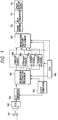
- Fig. 1 is a constructional diagram of the embodiment.
- reference numeral 101 denotes a lens; 102 a CCD; 103 an A/D converter; 104 an information distributing mechanism (distributing means); 105 a clock generator; 106 a CPU; 107 an information recovery mechanism (output control means); 108, 109, 110, and 111 memory blocks; 112 a frame memory; 113 a D/A converter; and 114 an image display device.
- image information (the total number of pixels of the image information is determined by the effective pixels of the CCD) whose image has been formed onto the CCD (pixels of the effective pixels) 102 by the lens 101 is converted into a digital signal by the A/D converter 103.
- An output of the A/D converter 103 is divided by the information distributing mechanism 104 on an m (n > m) pixel unit basis, for instance, a pixel unit basis of 2 x 2 pixels.
- the m pixels are divided on a p (m > p) pixel unit basis, for instance, one pixel unit basis.
- Each of the p pixels among the m pixels is distributed to m/p memory blocks 108 to 111, respectively. Inputs of the memory blocks are controlled synchronously with the clocks obtained by frequency dividing an output frequency of the A/D converter 103 that is controlled by the clock generator 105 into 1/4.
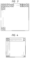
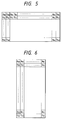
- the elements a xx , b xx , c xx , and d xx of (2 x 2) pixels of the original image in Fig. 3 are recorded into the respective memory blocks as image information in a format similar to that of the image consisting of only the element a xx shown in Fig. 4 which has been distributed.
- one memory block solely has the image information as shown in Fig. 4, in the case where addresses which are designated in the memory blocks are deviated by a few frames and the image information of different frames are respectively generated from the frames, by writing the image information into the addresses in the frame memory 112 by the information recovery mechanism 107 in Fig. 1 in a manner such that four images are displayed like a matric onto the image display device 114, four images can be simultaneously displayed.
- the image information that is finally generated is accumulated into the frame memory 112 and is converted into the analog information by the D/A converter 113 and outputted in accordance with a sync frequency of the image display device 114.
- reference numeral 201 denotes an encoding circuit; 202 a modulation circuit; 203 a substrate; 204 a cantilever type scanning mechanism; 205 a probe electrode; 206 a recording medium; 207 an XY scanning mechanism; 208 a demodulation circuit; 209 a decoding circuit; 210 a reading/writing circuit; and 211 an address generator.
- Four reading/writing circuits 210 and the cantilever type scanning mechanism are formed on the same substrate 203.
- the input information is BCH encoded by the encoding circuit 201 for error correction.
- an RZ modulation is executed by the modulation circuit 202.
- the modulated data is recorded onto the recoding medium 206 by the probe electrode 205 which has been moved to the position according to an output write address of the address generator 211 by the XY scanning mechanism 207.
- the recorded information is read out by the probe electrode which has been moved by the XY scanning mechanism 207 to the position according to the output read address of the address generator 211 (In this instance, the information is read out by detecting a change in tunnel current flowing in the probe electrode).
- the readout data is demodulated by the demodulation circuit 208 and is decoded by the decoding circuit 209 and is outputted.
- the recording medium 206 is manufactured as follows. That is, Au is epitaxially grown on a smooth substrate obtained by cleaving mica. Eight layers of squalillium-bis-6-octylazulene (hereinafter, abbreviated to SOAZ) having an electric memory effect are laminated on the Au substrate by a Langmuir-Blodgett (LB) method, thereby forming a recording layer as a recording medium 206.
- the recording medium 206 is constructed by the substrate and an underelectrode layer (not shown). Since the recording layer is made of a material having the memory effect for the switching characteristics of a voltage current, in the recording mode, it is sufficient to apply a pulse voltage of a waveform as shown in Fig.
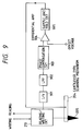
- the distance between the recording medium and the probe electrode is controlled as follows by using a control circuit of Fig. 9. Generally, a bias voltage of about 100 mV is applied between the recording medium and the probe electrode. The probe electrode is allowed to approach the recording medium by the cantilever type scanning mechanism 204 until a state in which a current of about 2 nA flows. The current detected by the probe electrode 205 is converted into the voltage signal by an I/V converting circuit 901. The signal passes through an LPF 902 whose cut-off frequency is set to about a scanning frequency so that the probe electrode can trace only the component of frequencies which are equal to or lower than the frequency upon scanning of the detection current signal due to an inclination on the substrate or the like.
- the signal is transmitted through a phase compensation circuit 903 and a difference between an output voltage of the phase compensation circuit 903 and an offset voltage is calculated by a differential amplifier 904 so that the distance between the probe electrode and the recording medium is set to a constant value as an average.
- the signal which has been transmitted through the above circuit is used to control the cantilever type scanning mechanism 204, thereby performing a feedback control.
- the distance between the probe electrode and the recording medium is set to a constant value.
- a sample and hold circuit 905 is set into a holding state by the feedback control so as not to cause a collision between them.
- the invention is not limited to them but other various methods which are generally used can be used.
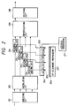
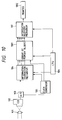
- FIG. 10 is a constructional diagram of the second embodiment.
- reference numeral 101 denotes the lens; 102 the CCD; 103 the A/D converter; 104 the information distributing mechanism; 105 the clock generator; 106 the CPU; 107 the information recovery mechanism; 1001 a group of memory blocks consisting of 25 memory blocks; and 1002 a printer.
- image information consisting of (2000 x 1125) pixels whose image has been formed on the CCD 102 by the lens 101 is converted into the digital signal by the A/D converter 103.
- An output of the A/D converter 103 is supplied to the information distributing mechanism 104, by which one information in (5 x 5) pixels is distributed into 25 memory blocks, respectively.
- the inputs of the memory blocks are controlled synchronously with clocks obtained by frequency dividing the output frequency of the A/D converter 103 that is controlled by the clock generator 105 into 1/5.
- the information recovery mechanism 107 In the printing mode, although the outputs of the memory blocks are controlled by similar clocks, in the information recovery mechanism 107, the input of one of the input channels is permitted by the CPU 106 in case of a single print. From the data of the permitted input channel, the information recovery mechanism 107 outputs the image information and can print at a high speed. By making the output images of the memory blocks different, a plurality of images can be continuously outputted at a high speed.
- the original image is distributed into 1/5 in each of the vertical and lateral directions, it is optimum to a printer having a resolution of about 400 d.p.i.. If the outputs of all of the channels are set to the outputs of the same frame, they can be outputted to a printer of a high precision or a conventional method whereby a resolution is reduced by executing processes in a software manner can be also used.
- the operations in the memory block are similar to those in the first embodiment.
Landscapes
- Chemical & Material Sciences (AREA)
- Nanotechnology (AREA)
- Engineering & Computer Science (AREA)
- Crystallography & Structural Chemistry (AREA)
- Molecular Biology (AREA)
- General Health & Medical Sciences (AREA)
- Health & Medical Sciences (AREA)
- Life Sciences & Earth Sciences (AREA)
- Image Processing (AREA)
- Television Signal Processing For Recording (AREA)
- Debugging And Monitoring (AREA)
- Signal Processing For Digital Recording And Reproducing (AREA)
- Optical Recording Or Reproduction (AREA)
Applications Claiming Priority (2)
| Application Number | Priority Date | Filing Date | Title |
|---|---|---|---|
| JP293906/91 | 1991-10-15 | ||
| JP03293906A JP3118658B2 (ja) | 1991-10-15 | 1991-10-15 | 情報処理装置 |
Publications (3)
| Publication Number | Publication Date |
|---|---|
| EP0541978A2 true EP0541978A2 (de) | 1993-05-19 |
| EP0541978A3 EP0541978A3 (en) | 1993-11-10 |
| EP0541978B1 EP0541978B1 (de) | 1998-06-10 |
Family
ID=17800686
Family Applications (1)
| Application Number | Title | Priority Date | Filing Date |
|---|---|---|---|
| EP92117452A Expired - Lifetime EP0541978B1 (de) | 1991-10-15 | 1992-10-13 | Informationsverarbeitungsgerät |
Country Status (6)
| Country | Link |
|---|---|
| US (1) | US5535018A (de) |
| EP (1) | EP0541978B1 (de) |
| JP (1) | JP3118658B2 (de) |
| AT (1) | ATE167328T1 (de) |
| CA (1) | CA2080252C (de) |
| DE (1) | DE69225865T2 (de) |
Cited By (4)
| Publication number | Priority date | Publication date | Assignee | Title |
|---|---|---|---|---|
| WO1995013601A1 (en) * | 1993-11-09 | 1995-05-18 | Honeywell Inc. | Partitioned display apparatus |
| WO1995013604A1 (en) * | 1993-11-09 | 1995-05-18 | Honeywell Inc. | Reconfigurable graphics memory architecture for display apparatus |
| WO2000065565A1 (en) * | 1999-04-23 | 2000-11-02 | Opti, Inc. | High resolution display controller with reduced working frequency requirement for the display data handling circuitry |
| WO2010043252A1 (de) * | 2008-10-15 | 2010-04-22 | Siemens Ag Österreich | Verfahren und system zur ermittlung einer fahrzeuggeschwindigkeit |
Families Citing this family (11)
| Publication number | Priority date | Publication date | Assignee | Title |
|---|---|---|---|---|
| JPH0450256U (de) * | 1990-09-05 | 1992-04-28 | ||
| KR100205009B1 (ko) | 1996-04-17 | 1999-06-15 | 윤종용 | 비디오신호 변환장치 및 그 장치를 구비한 표시장치 |
| KR100204334B1 (ko) * | 1996-07-05 | 1999-06-15 | 윤종용 | 표시모드 변환기능을 갖는 비디오신호 변환장치 및 그 장치를 구비한 표시장치 |
| US5796392A (en) | 1997-02-24 | 1998-08-18 | Paradise Electronics, Inc. | Method and apparatus for clock recovery in a digital display unit |
| US6018597A (en) * | 1997-03-21 | 2000-01-25 | Intermec Ip Corporation | Method and apparatus for changing or mapping video or digital images from one image density to another |
| JPH10312592A (ja) * | 1997-05-13 | 1998-11-24 | Canon Inc | 情報処理装置および情報処理方法 |
| US5987192A (en) * | 1997-09-18 | 1999-11-16 | Intermec Ip Corporation | Method and apparatus for processing or resizing digital images, such as images of bar code symbols |
| JP2002310882A (ja) * | 2001-04-17 | 2002-10-23 | Canon Inc | 走査型プローブによる信号検出装置、該装置によるプローブ顕微鏡、及び走査型プローブによる信号検出方法、該方法を用いてサンプル表面を観察する観察方法 |
| JP4393135B2 (ja) * | 2003-08-22 | 2010-01-06 | キヤノン株式会社 | 放射線画像処理装置、放射線画像処理方法、コンピュータプログラム、及びコンピュータ読み取り可能な記録媒体 |
| US7567235B2 (en) * | 2005-12-12 | 2009-07-28 | Cypress Semiconductor Corporation | Self-aligning optical sensor package |
| US7486403B2 (en) * | 2006-07-20 | 2009-02-03 | Canon Kabushiki Kaisha | Droplet shape measuring method and apparatus |
Family Cites Families (9)
| Publication number | Priority date | Publication date | Assignee | Title |
|---|---|---|---|---|
| DE3141882A1 (de) * | 1981-10-22 | 1983-05-05 | Agfa-Gevaert Ag, 5090 Leverkusen | Dynamische schreib- und lesespeichervorrichtung |
| GB2199982B (en) * | 1987-01-14 | 1991-09-11 | Rca Corp | Segmented tape format video tape system |
| GB2213345B (en) * | 1987-12-28 | 1992-01-15 | Mitsubishi Electric Corp | Image data filing system |
| DE68929194T2 (de) * | 1988-01-08 | 2000-09-28 | Fuji Photo Film Co., Ltd. | Gerät zur Farbfilmanalyse |
| JPH02249380A (ja) * | 1989-03-22 | 1990-10-05 | Toshiba Corp | 画像記録再生装置 |
| JPH03153161A (ja) * | 1989-11-10 | 1991-07-01 | Canon Inc | 画像伝送装置 |
| JP2925214B2 (ja) * | 1990-01-24 | 1999-07-28 | キヤノン株式会社 | 画像信号記録及び再生装置 |
| US5148497A (en) * | 1990-02-14 | 1992-09-15 | Massachusetts Institute Of Technology | Fractal-based image compression and interpolation |
| US5062136A (en) * | 1990-09-12 | 1991-10-29 | The United States Of America As Represented By The Secretary Of The Navy | Telecommunications system and method |
-
1991
- 1991-10-15 JP JP03293906A patent/JP3118658B2/ja not_active Expired - Fee Related
-
1992
- 1992-10-09 CA CA002080252A patent/CA2080252C/en not_active Expired - Fee Related
- 1992-10-13 DE DE69225865T patent/DE69225865T2/de not_active Expired - Fee Related
- 1992-10-13 EP EP92117452A patent/EP0541978B1/de not_active Expired - Lifetime
- 1992-10-13 AT AT92117452T patent/ATE167328T1/de not_active IP Right Cessation
-
1995
- 1995-11-30 US US08/565,013 patent/US5535018A/en not_active Expired - Lifetime
Cited By (5)
| Publication number | Priority date | Publication date | Assignee | Title |
|---|---|---|---|---|
| WO1995013601A1 (en) * | 1993-11-09 | 1995-05-18 | Honeywell Inc. | Partitioned display apparatus |
| WO1995013604A1 (en) * | 1993-11-09 | 1995-05-18 | Honeywell Inc. | Reconfigurable graphics memory architecture for display apparatus |
| US5530457A (en) * | 1993-11-09 | 1996-06-25 | Honeywell Inc. | Partitioned display apparatus |
| WO2000065565A1 (en) * | 1999-04-23 | 2000-11-02 | Opti, Inc. | High resolution display controller with reduced working frequency requirement for the display data handling circuitry |
| WO2010043252A1 (de) * | 2008-10-15 | 2010-04-22 | Siemens Ag Österreich | Verfahren und system zur ermittlung einer fahrzeuggeschwindigkeit |
Also Published As
| Publication number | Publication date |
|---|---|
| EP0541978A3 (en) | 1993-11-10 |
| US5535018A (en) | 1996-07-09 |
| EP0541978B1 (de) | 1998-06-10 |
| DE69225865T2 (de) | 1999-01-28 |
| CA2080252A1 (en) | 1993-04-16 |
| CA2080252C (en) | 1999-01-12 |
| JPH05109129A (ja) | 1993-04-30 |
| DE69225865D1 (de) | 1998-07-16 |
| JP3118658B2 (ja) | 2000-12-18 |
| ATE167328T1 (de) | 1998-06-15 |
Similar Documents
| Publication | Publication Date | Title |
|---|---|---|
| US5535018A (en) | Information processing apparatus | |
| JP3073616B2 (ja) | マルチプローブを具備する情報処理装置 | |
| JP3246987B2 (ja) | マルチプローブ制御回路を具備する情報処理装置 | |
| EP0468456A2 (de) | Informationsaufzeichnungs- und/oder Wiedergabegerät | |
| EP0603705B1 (de) | Gerät zur Verarbeitung eines Bildsignales | |
| JP2783672B2 (ja) | 情報記録及び/又は再生方法と情報記録及び/又は再生装置 | |
| US5510858A (en) | Television receiver having an STM memory | |
| US5404349A (en) | Position displacement detecting apparatus | |
| JP2744338B2 (ja) | 情報読取り及び/又は入力を行なう装置及び方法 | |
| JP3029143B2 (ja) | 情報再生方法 | |
| JP3135753B2 (ja) | プローブを用いた記録再生方法および装置 | |
| US5995704A (en) | Information processing apparatus capable of readily changing resolution | |
| US5581364A (en) | Method for recording and/or reproducing image signals and an apparatus therefor utilizing two dimensional scanning of a recording medium by a probe | |
| JP3053142B2 (ja) | 情報処理装置 | |
| JP3129860B2 (ja) | 画像信号処理機構およびその適用機器 | |
| JP2994808B2 (ja) | 記録方法及び記録装置 | |
| JP3095915B2 (ja) | 情報処理装置 | |
| CA2035996C (en) | Position displacement detecting apparatus | |
| JP3004823B2 (ja) | 情報処理装置 | |
| JP3039725B2 (ja) | 情報処理装置 | |
| JPH08249733A (ja) | 情報処理装置 | |
| JP4079397B2 (ja) | 記録再生装置のトラッキング機構及びトラッキング方法 | |
| JP3093946B2 (ja) | 記録媒体 | |
| JP2968610B2 (ja) | 情報記録再生装置 | |
| JPH05120741A (ja) | 情報処理装置 |
Legal Events
| Date | Code | Title | Description |
|---|---|---|---|
| PUAI | Public reference made under article 153(3) epc to a published international application that has entered the european phase |
Free format text: ORIGINAL CODE: 0009012 |
|
| AK | Designated contracting states |
Kind code of ref document: A2 Designated state(s): AT BE CH DE DK ES FR GB GR IT LI LU MC NL PT SE |
|
| PUAL | Search report despatched |
Free format text: ORIGINAL CODE: 0009013 |
|
| AK | Designated contracting states |
Kind code of ref document: A3 Designated state(s): AT BE CH DE DK ES FR GB GR IT LI LU MC NL PT SE |
|
| 17P | Request for examination filed |
Effective date: 19940324 |
|
| 17Q | First examination report despatched |
Effective date: 19951019 |
|
| GRAG | Despatch of communication of intention to grant |
Free format text: ORIGINAL CODE: EPIDOS AGRA |
|
| GRAG | Despatch of communication of intention to grant |
Free format text: ORIGINAL CODE: EPIDOS AGRA |
|
| GRAG | Despatch of communication of intention to grant |
Free format text: ORIGINAL CODE: EPIDOS AGRA |
|
| GRAH | Despatch of communication of intention to grant a patent |
Free format text: ORIGINAL CODE: EPIDOS IGRA |
|
| GRAH | Despatch of communication of intention to grant a patent |
Free format text: ORIGINAL CODE: EPIDOS IGRA |
|
| GRAA | (expected) grant |
Free format text: ORIGINAL CODE: 0009210 |
|
| AK | Designated contracting states |
Kind code of ref document: B1 Designated state(s): AT BE CH DE DK ES FR GB GR IT LI LU MC NL PT SE |
|
| PG25 | Lapsed in a contracting state [announced via postgrant information from national office to epo] |
Ref country code: ES Free format text: THE PATENT HAS BEEN ANNULLED BY A DECISION OF A NATIONAL AUTHORITY Effective date: 19980610 Ref country code: GR Free format text: LAPSE BECAUSE OF FAILURE TO SUBMIT A TRANSLATION OF THE DESCRIPTION OR TO PAY THE FEE WITHIN THE PRESCRIBED TIME-LIMIT Effective date: 19980610 Ref country code: BE Free format text: LAPSE BECAUSE OF FAILURE TO SUBMIT A TRANSLATION OF THE DESCRIPTION OR TO PAY THE FEE WITHIN THE PRESCRIBED TIME-LIMIT Effective date: 19980610 Ref country code: LI Free format text: LAPSE BECAUSE OF FAILURE TO SUBMIT A TRANSLATION OF THE DESCRIPTION OR TO PAY THE FEE WITHIN THE PRESCRIBED TIME-LIMIT Effective date: 19980610 Ref country code: CH Free format text: LAPSE BECAUSE OF FAILURE TO SUBMIT A TRANSLATION OF THE DESCRIPTION OR TO PAY THE FEE WITHIN THE PRESCRIBED TIME-LIMIT Effective date: 19980610 Ref country code: AT Free format text: LAPSE BECAUSE OF FAILURE TO SUBMIT A TRANSLATION OF THE DESCRIPTION OR TO PAY THE FEE WITHIN THE PRESCRIBED TIME-LIMIT Effective date: 19980610 Ref country code: NL Free format text: LAPSE BECAUSE OF FAILURE TO SUBMIT A TRANSLATION OF THE DESCRIPTION OR TO PAY THE FEE WITHIN THE PRESCRIBED TIME-LIMIT Effective date: 19980610 |
|
| REF | Corresponds to: |
Ref document number: 167328 Country of ref document: AT Date of ref document: 19980615 Kind code of ref document: T |
|
| REG | Reference to a national code |
Ref country code: CH Ref legal event code: EP |
|
| REF | Corresponds to: |
Ref document number: 69225865 Country of ref document: DE Date of ref document: 19980716 |
|
| ITF | It: translation for a ep patent filed | ||
| ET | Fr: translation filed | ||
| PG25 | Lapsed in a contracting state [announced via postgrant information from national office to epo] |
Ref country code: DK Free format text: LAPSE BECAUSE OF FAILURE TO SUBMIT A TRANSLATION OF THE DESCRIPTION OR TO PAY THE FEE WITHIN THE PRESCRIBED TIME-LIMIT Effective date: 19980910 Ref country code: SE Free format text: LAPSE BECAUSE OF FAILURE TO SUBMIT A TRANSLATION OF THE DESCRIPTION OR TO PAY THE FEE WITHIN THE PRESCRIBED TIME-LIMIT Effective date: 19980910 |
|
| PG25 | Lapsed in a contracting state [announced via postgrant information from national office to epo] |
Ref country code: PT Free format text: LAPSE BECAUSE OF FAILURE TO SUBMIT A TRANSLATION OF THE DESCRIPTION OR TO PAY THE FEE WITHIN THE PRESCRIBED TIME-LIMIT Effective date: 19980915 |
|
| PG25 | Lapsed in a contracting state [announced via postgrant information from national office to epo] |
Ref country code: LU Free format text: LAPSE BECAUSE OF NON-PAYMENT OF DUE FEES Effective date: 19981013 |
|
| NLV1 | Nl: lapsed or annulled due to failure to fulfill the requirements of art. 29p and 29m of the patents act | ||
| REG | Reference to a national code |
Ref country code: CH Ref legal event code: PL |
|
| PLBE | No opposition filed within time limit |
Free format text: ORIGINAL CODE: 0009261 |
|
| STAA | Information on the status of an ep patent application or granted ep patent |
Free format text: STATUS: NO OPPOSITION FILED WITHIN TIME LIMIT |
|
| PG25 | Lapsed in a contracting state [announced via postgrant information from national office to epo] |
Ref country code: MC Free format text: LAPSE BECAUSE OF NON-PAYMENT OF DUE FEES Effective date: 19990430 |
|
| 26N | No opposition filed | ||
| REG | Reference to a national code |
Ref country code: GB Ref legal event code: IF02 |
|
| PGFP | Annual fee paid to national office [announced via postgrant information from national office to epo] |
Ref country code: DE Payment date: 20081031 Year of fee payment: 17 |
|
| PGFP | Annual fee paid to national office [announced via postgrant information from national office to epo] |
Ref country code: IT Payment date: 20081020 Year of fee payment: 17 |
|
| PGFP | Annual fee paid to national office [announced via postgrant information from national office to epo] |
Ref country code: FR Payment date: 20081024 Year of fee payment: 17 |
|
| PGFP | Annual fee paid to national office [announced via postgrant information from national office to epo] |
Ref country code: GB Payment date: 20081029 Year of fee payment: 17 |
|
| REG | Reference to a national code |
Ref country code: FR Ref legal event code: ST Effective date: 20100630 |
|
| PG25 | Lapsed in a contracting state [announced via postgrant information from national office to epo] |
Ref country code: DE Free format text: LAPSE BECAUSE OF NON-PAYMENT OF DUE FEES Effective date: 20100501 Ref country code: FR Free format text: LAPSE BECAUSE OF NON-PAYMENT OF DUE FEES Effective date: 20091102 |
|
| PG25 | Lapsed in a contracting state [announced via postgrant information from national office to epo] |
Ref country code: GB Free format text: LAPSE BECAUSE OF NON-PAYMENT OF DUE FEES Effective date: 20091013 |
|
| PG25 | Lapsed in a contracting state [announced via postgrant information from national office to epo] |
Ref country code: IT Free format text: LAPSE BECAUSE OF NON-PAYMENT OF DUE FEES Effective date: 20091013 |