EP0542533A1 - Halbleiterträger zum stabilen Montieren eines Halbleiterchips - Google Patents
Halbleiterträger zum stabilen Montieren eines Halbleiterchips Download PDFInfo
- Publication number
- EP0542533A1 EP0542533A1 EP92310311A EP92310311A EP0542533A1 EP 0542533 A1 EP0542533 A1 EP 0542533A1 EP 92310311 A EP92310311 A EP 92310311A EP 92310311 A EP92310311 A EP 92310311A EP 0542533 A1 EP0542533 A1 EP 0542533A1
- Authority
- EP
- European Patent Office
- Prior art keywords
- electrode leads
- chip carrier
- electrode
- board
- corners
- Prior art date
- Legal status (The legal status is an assumption and is not a legal conclusion. Google has not performed a legal analysis and makes no representation as to the accuracy of the status listed.)
- Withdrawn
Links
Images



Classifications
-
- H—ELECTRICITY
- H10—SEMICONDUCTOR DEVICES; ELECTRIC SOLID-STATE DEVICES NOT OTHERWISE PROVIDED FOR
- H10W—GENERIC PACKAGES, INTERCONNECTIONS, CONNECTORS OR OTHER CONSTRUCTIONAL DETAILS OF DEVICES COVERED BY CLASS H10
- H10W70/00—Package substrates; Interposers; Redistribution layers [RDL]
- H10W70/60—Insulating or insulated package substrates; Interposers; Redistribution layers
- H10W70/62—Insulating or insulated package substrates; Interposers; Redistribution layers characterised by their interconnections
- H10W70/65—Shapes or dispositions of interconnections
-
- H—ELECTRICITY
- H05—ELECTRIC TECHNIQUES NOT OTHERWISE PROVIDED FOR
- H05K—PRINTED CIRCUITS; CASINGS OR CONSTRUCTIONAL DETAILS OF ELECTRIC APPARATUS; MANUFACTURE OF ASSEMBLAGES OF ELECTRICAL COMPONENTS
- H05K3/00—Apparatus or processes for manufacturing printed circuits
- H05K3/30—Assembling printed circuits with electric components, e.g. with resistors
- H05K3/32—Assembling printed circuits with electric components, e.g. with resistors electrically connecting electric components or wires to printed circuits
- H05K3/34—Assembling printed circuits with electric components, e.g. with resistors electrically connecting electric components or wires to printed circuits by soldering
- H05K3/341—Surface mounted components
- H05K3/3431—Leadless components
- H05K3/3442—Leadless components having edge contacts, e.g. leadless chip capacitors, chip carriers
-
- H—ELECTRICITY
- H10—SEMICONDUCTOR DEVICES; ELECTRIC SOLID-STATE DEVICES NOT OTHERWISE PROVIDED FOR
- H10W—GENERIC PACKAGES, INTERCONNECTIONS, CONNECTORS OR OTHER CONSTRUCTIONAL DETAILS OF DEVICES COVERED BY CLASS H10
- H10W70/00—Package substrates; Interposers; Redistribution layers [RDL]
- H10W70/60—Insulating or insulated package substrates; Interposers; Redistribution layers
- H10W70/62—Insulating or insulated package substrates; Interposers; Redistribution layers characterised by their interconnections
- H10W70/65—Shapes or dispositions of interconnections
- H10W70/657—Shapes or dispositions of interconnections on sidewalls or bottom surfaces of the package substrates, interposers or redistribution layers
-
- H—ELECTRICITY
- H05—ELECTRIC TECHNIQUES NOT OTHERWISE PROVIDED FOR
- H05K—PRINTED CIRCUITS; CASINGS OR CONSTRUCTIONAL DETAILS OF ELECTRIC APPARATUS; MANUFACTURE OF ASSEMBLAGES OF ELECTRICAL COMPONENTS
- H05K1/00—Printed circuits
- H05K1/02—Details
- H05K1/11—Printed elements for providing electric connections to or between printed circuits
- H05K1/111—Pads for surface mounting, e.g. lay-out
-
- H—ELECTRICITY
- H05—ELECTRIC TECHNIQUES NOT OTHERWISE PROVIDED FOR
- H05K—PRINTED CIRCUITS; CASINGS OR CONSTRUCTIONAL DETAILS OF ELECTRIC APPARATUS; MANUFACTURE OF ASSEMBLAGES OF ELECTRICAL COMPONENTS
- H05K2201/00—Indexing scheme relating to printed circuits covered by H05K1/00
- H05K2201/09—Shape and layout
- H05K2201/09145—Edge details
- H05K2201/09181—Notches in edge pads
-
- H—ELECTRICITY
- H05—ELECTRIC TECHNIQUES NOT OTHERWISE PROVIDED FOR
- H05K—PRINTED CIRCUITS; CASINGS OR CONSTRUCTIONAL DETAILS OF ELECTRIC APPARATUS; MANUFACTURE OF ASSEMBLAGES OF ELECTRICAL COMPONENTS
- H05K2201/00—Indexing scheme relating to printed circuits covered by H05K1/00
- H05K2201/09—Shape and layout
- H05K2201/09209—Shape and layout details of conductors
- H05K2201/09372—Pads and lands
- H05K2201/09381—Shape of non-curved single flat metallic pad, land or exposed part thereof; Shape of electrode of leadless component
-
- H—ELECTRICITY
- H05—ELECTRIC TECHNIQUES NOT OTHERWISE PROVIDED FOR
- H05K—PRINTED CIRCUITS; CASINGS OR CONSTRUCTIONAL DETAILS OF ELECTRIC APPARATUS; MANUFACTURE OF ASSEMBLAGES OF ELECTRICAL COMPONENTS
- H05K2201/00—Indexing scheme relating to printed circuits covered by H05K1/00
- H05K2201/09—Shape and layout
- H05K2201/09209—Shape and layout details of conductors
- H05K2201/09372—Pads and lands
- H05K2201/094—Array of pads or lands differing from one another, e.g. in size, pitch or thickness; Using different connections on the pads
-
- H—ELECTRICITY
- H05—ELECTRIC TECHNIQUES NOT OTHERWISE PROVIDED FOR
- H05K—PRINTED CIRCUITS; CASINGS OR CONSTRUCTIONAL DETAILS OF ELECTRIC APPARATUS; MANUFACTURE OF ASSEMBLAGES OF ELECTRICAL COMPONENTS
- H05K2201/00—Indexing scheme relating to printed circuits covered by H05K1/00
- H05K2201/10—Details of components or other objects attached to or integrated in a printed circuit board
- H05K2201/10613—Details of electrical connections of non-printed components, e.g. special leads
- H05K2201/10621—Components characterised by their electrical contacts
- H05K2201/10727—Leadless chip carrier [LCC], e.g. chip-modules for cards
-
- H—ELECTRICITY
- H10—SEMICONDUCTOR DEVICES; ELECTRIC SOLID-STATE DEVICES NOT OTHERWISE PROVIDED FOR
- H10W—GENERIC PACKAGES, INTERCONNECTIONS, CONNECTORS OR OTHER CONSTRUCTIONAL DETAILS OF DEVICES COVERED BY CLASS H10
- H10W70/00—Package substrates; Interposers; Redistribution layers [RDL]
- H10W70/60—Insulating or insulated package substrates; Interposers; Redistribution layers
- H10W70/67—Insulating or insulated package substrates; Interposers; Redistribution layers characterised by their insulating layers or insulating parts
- H10W70/68—Shapes or dispositions thereof
- H10W70/682—Shapes or dispositions thereof comprising holes having chips therein
-
- H—ELECTRICITY
- H10—SEMICONDUCTOR DEVICES; ELECTRIC SOLID-STATE DEVICES NOT OTHERWISE PROVIDED FOR
- H10W—GENERIC PACKAGES, INTERCONNECTIONS, CONNECTORS OR OTHER CONSTRUCTIONAL DETAILS OF DEVICES COVERED BY CLASS H10
- H10W72/00—Interconnections or connectors in packages
- H10W72/851—Dispositions of multiple connectors or interconnections
- H10W72/874—On different surfaces
- H10W72/884—Die-attach connectors and bond wires
-
- H—ELECTRICITY
- H10—SEMICONDUCTOR DEVICES; ELECTRIC SOLID-STATE DEVICES NOT OTHERWISE PROVIDED FOR
- H10W—GENERIC PACKAGES, INTERCONNECTIONS, CONNECTORS OR OTHER CONSTRUCTIONAL DETAILS OF DEVICES COVERED BY CLASS H10
- H10W74/00—Encapsulations, e.g. protective coatings
-
- H—ELECTRICITY
- H10—SEMICONDUCTOR DEVICES; ELECTRIC SOLID-STATE DEVICES NOT OTHERWISE PROVIDED FOR
- H10W—GENERIC PACKAGES, INTERCONNECTIONS, CONNECTORS OR OTHER CONSTRUCTIONAL DETAILS OF DEVICES COVERED BY CLASS H10
- H10W90/00—Package configurations
- H10W90/701—Package configurations characterised by the relative positions of pads or connectors relative to package parts
- H10W90/731—Package configurations characterised by the relative positions of pads or connectors relative to package parts of die-attach connectors
- H10W90/734—Package configurations characterised by the relative positions of pads or connectors relative to package parts of die-attach connectors between a chip and a stacked insulating package substrate, interposer or RDL
-
- H—ELECTRICITY
- H10—SEMICONDUCTOR DEVICES; ELECTRIC SOLID-STATE DEVICES NOT OTHERWISE PROVIDED FOR
- H10W—GENERIC PACKAGES, INTERCONNECTIONS, CONNECTORS OR OTHER CONSTRUCTIONAL DETAILS OF DEVICES COVERED BY CLASS H10
- H10W90/00—Package configurations
- H10W90/701—Package configurations characterised by the relative positions of pads or connectors relative to package parts
- H10W90/751—Package configurations characterised by the relative positions of pads or connectors relative to package parts of bond wires
- H10W90/754—Package configurations characterised by the relative positions of pads or connectors relative to package parts of bond wires between a chip and a stacked insulating package substrate, interposer or RDL
-
- Y—GENERAL TAGGING OF NEW TECHNOLOGICAL DEVELOPMENTS; GENERAL TAGGING OF CROSS-SECTIONAL TECHNOLOGIES SPANNING OVER SEVERAL SECTIONS OF THE IPC; TECHNICAL SUBJECTS COVERED BY FORMER USPC CROSS-REFERENCE ART COLLECTIONS [XRACs] AND DIGESTS
- Y02—TECHNOLOGIES OR APPLICATIONS FOR MITIGATION OR ADAPTATION AGAINST CLIMATE CHANGE
- Y02P—CLIMATE CHANGE MITIGATION TECHNOLOGIES IN THE PRODUCTION OR PROCESSING OF GOODS
- Y02P70/00—Climate change mitigation technologies in the production process for final industrial or consumer products
- Y02P70/50—Manufacturing or production processes characterised by the final manufactured product
Definitions
- the present invention relates to a semiconductor chip carrier for use in supporting a semiconductor chip, and to a semiconductor device and an apparatus which includes the semiconductor chip carrier and the semiconductor device, respectively.
- a semiconductor chip carrier has been used in the field of semiconductor assembly technique.
- a chip carrier of plastic LCC (Leadless Chip Carrier) type has recently attracted considerable attention as a chip carrier which is applicable to a high density assembly in a circuit board, because it makes it possible to become as thin as substantially 1mm.
- a conventional LCC type chip carrier comprises an insulating substrate which has a rectangular shape having four corners and which has a central surface and a peripheral surface surrounding the central surface, and a plurality of electrode leads deposited on the peripheral surface.
- a semiconductor chip is mounted on the central surface of the insulating substrate to form a semiconductor device.
- the insulating substrate is further mounted on a circuit board which has a plurality of board electrodes on a board surface. The board electrodes are electrically connected to the electrode leads on the chip carrier by the use of solder.
- the chip carrier is mounted on the circuit board.
- each electrode lead should be connected to each board electrode through a very small contact area.
- strength of connection between the solder and each electrode lead becomes weak with a decrease of the area between the solder and each electrode lead.
- the strength of connection by the solder is 500g/mm2
- the strength of 60g per one electrode lead is acquired when the area of contact of the solder per one electrode lead is as small as 0.12mm2 (0.3 x 0.4 mm2).
- the number of electrode leads is between 50 and 80, the strength of connecting the package to the circuit board, as a whole, merely falls within a range between 3kg and 5kg. Thus, the strength of the whole connection is not so small.
- a stress sometimes acts on the circuit board during or after an assembly process.
- the circuit board is sometimes twisted or warped as a result of the stress. Since the stress is concentrated on each electrode lead positioned at each of the four corners of the rectangular insulating substrate of the chip carrier, the electrode leads positioned thereat often come off the board electrodes by such a twist or warp of the circuit board. Thus, it often happens that the electrode leads are peeled off from the board electrodes at the four corners of the insulating substrate.
- the chip carrier is mounted on the circuit board which is known as a thin-type circuit board for a high density assembly and which has a thickness thinner than 0.6mm, such a circuit board is apt to be easily twisted or warped during or after the assembly process. Therefore, the problem that the electrode leads come off the board electrodes is very serious in such a thin-type circuit board.
- an improved semiconductor chip carrier which is for use in supporting a semiconductor chip is provided.
- the invention provides a chip carrier for use in supporting a semiconductor chip; said chip carrier comprising: an insulating substrate which has a central portion having a primary surface and a peripheral portion having a secondary surface surrounding said primary surface; electrode leads disposed at positions distributed around the edges of the substrate, the shape of the substrate being such that some of the electrode leads are at positions at which, in the event of distortion of the substrate, greater stresses are imposed on those electrode leads than on the remainder thereof, characterised in that the electrode leads at said positions are wider than the remaining electrode leads.
- the substrate may be polygonal, the wider electrode leads may include those at positions nearest corners of the substrate.
- the invention comprises an insulating substrate which has a substantially rectangular shape having four corners and which has a central portion having a primary surface and a peripheral portion having a secondary surface surrounding the primary surface, and electrode leads deposited on the secondary surface, and electrode leads deposited on the secondary surface; wherein the electrode leads comprises: first electrode leads positioned remote from the four corners and each of which has a first predetermined width; and second electrode leads each of which is adjacent to each of the corners in comparison with the first electrode leads and each of which has a second width wider than the first width.
- the second electrode leads may be equal in number to four; each second electrode lead being located on each four corner.
- the second electrode leads may also be equal in number to eight; the eight second electrode leads being located on both sides of each of the four corners with each corner interposed therebetween.
- the invention provides a semiconductor device comprising a chip corner as set forth above, a semiconductor chip which is mounted on the primary surface of the corner and which has a selected one of an IC circuit, an LSI circuit and a VLSI circuit; and a plurality of chip electrodes; and connection means for connecting said chip electrodes to the electrode leads of the carrier.
- the invention also provides a semiconductor apparatus comprising: a circuit board which has a board surface and a plurality of board electrodes; a semiconductor device as set forth above, and further connection means for connecting said board electrodes to the electrode leads of the chip carrier.
- FIGs. 1(A) and (B) a conventional semiconductor chip carrier will first be described for a better understanding of this invention.
- a semiconductor chip carrier 1 which is a plastic LCC type one.
- the semiconductor chip carrier 1 comprises an insulating substrate 2 which is made of a glass epoxy resin plate.
- a predetermined direction may be defined from the lefthand side of Fig. 1 to the righthand side thereof on the insulating substrate 2 for brevity of description.
- the insulating substrate 2 also has two sides 3, 3 which are parallel to the predetermined direction and the other two sides 4, 4 which are orthogonal to the predetermined direction. Formed by the sides 3, 3 and 4, 4, the insulating substrate 2 has a substantially rectangular shape which has four corners 2a, 2b, 2c, and 2d.
- the insulating substrate 2 also has a central portion 5 having a primary surface 5a and a peripheral portion 6 having a secondary surface 6a which surrounds the primary surface 5a.
- the primary surface 5a is offset from the secondary surface 6a to form a recess 7 in which a semiconductor chip is mounted.
- the peripheral portion 6 has a plurality of grooves 8 which are aligned at equal spaces in each side surface of the peripheral portion 6.
- Each of the electrode leads 9 has a predetermined or uniform width such as 0.3mm.
- Figs. 2(A) and (B) description will be made as to an assembly process of a semiconductor apparatus, namely, a method of mounting a semiconductor chip to a circuit board through the chip carrier 1 illustrated in Fig. 1.
- the semiconductor chip 10 may have a circuit (not shown), such as selected one of an IC circuit, an LSI circuit, and a VLSI circuit and a plurality of chip electrodes 12 electrically connected to the circuit. As illustrated in Figs. 2(A) and (B), the semiconductor chip 10 is mounted on the primary surface 5a formed by the recess 7. The chip electrodes 12 are then connected to the electrode leads 9 through first connection elements, such as bonding wires 13, 13.
- a resin frame 14 rests on the portions of the electrode leads 9 which are positioned on the secondary surface 6a of the peripheral portion 6 through a layer 15 which protects the electrode leads 9 from the resin frame 14.
- the area surrounded by the resin frame 14 is then filled with resin 16 to cover the semiconductor chip 10 with the resin 16 airtightly.
- the semiconductor device 11 is manufactured by a combination of the chip carrier 1 and the semiconductor chip 10.
- the circuit board 17 has a thickness which is not more than 0.6mm, a board surface 19, and a plurality of board electrodes 20 deposited on the board surface 19. Solder paste regions, as second connection elements, are printed on the board electrodes 20.
- the chip carrier 1 is then mounted on the circuit board 17 with the electrode leads 9 electrically connected to the corresponding board electrodes 20. In this event, the electrode leads 9 are also connected to the board electrodes 20 through solder masses 21 which serves as second connection elements by a solder reflow method.
- the semiconductor apparatus 18 is formed by a combination of the semiconductor device 11 and the circuit board 17.
- the illustrated semiconductor chip carrier comprises some parts which are similar to those of the above-described conventional semiconductor chip carrier and which are represented by the common reference numerals.
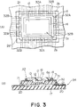
- the semiconductor chip carrier 31 illustrated in Figs. 3(A) and (B) also comprises the insulating substrate 2.
- a plurality of electrode leads 32 are deposited such that each electrode lead 32 is perpendicular to each side of the insulating substrate 2 and that each electrode lead 32 is extended into each groove 8.
- the electrode leads 32 comprises first electrode leads 32A positioned remote from the four corners 2a, 2b, 2c, and 2d and second electrode leads 32B each of which is adjacent to each of the corners 2a, 2b, 2c, and 2d.
- the second electrode leads 32B are equal in number to four and are located at the four corners 2a, 2b, 2c, and 2d, respectively.
- each of the first electrode leads 32A has a first predetermined or uniform width.
- each of the second electrode leads 32B has a second width wider than the first predetermined or uniform width. Specifically, the second width is approximately 0.6mm while the first width is approximately 0.3mm, in the illustrated example.
- each of the first electrode leads and the second electrode leads has a predetermined length of about 0.4mm.
- the semiconductor chip 10 is, at first, mounted to the chip carrier 31 to form a semiconductor device 33.
- a resin frame 14 rests on the portions of the electrode leads 32 which are positioned on the secondary surface 6a through the layer 15.
- the area surrounded by the resin frame 14 is then filled with the resin 16 to cover the semiconductor chip 10 with the resin 16 airtightly.
- the semiconductor device 33 is manufactured by a combination of the chip carrier 31 and the semiconductor chip 10.
- the semiconductor device 33 is mounted onto the circuit board 17 to form a semiconductor apparatus 34.
- the chip carrier 31 is mounted on the circuit board 17 with the electrode leads 32 electrically connected to the corresponding board electrodes 20.
- the electrode leads 32 are also connected to the board electrodes 20 through the solder masses 21 by the solder reflow method.
- the semiconductor apparatus 34 is formed by a combination of the semiconductor device 33 and the circuit board 17.
- each electrode lead 32B positioned thereat has the second width of approximately 0.6mm equal to twice the first width. Accordingly, the area of contact of the solder 21 per one electrode lead 32B is as wide as 0.24mm2 (0.6 x 0.4 mm2) while the area of contact of the solder 21 per one electrode lead 32A is as narrow as 0.12 mm2 (0.3 x 0.4 mm2). Each electrode lead 32B is therefore strongly connected to the corresponding board electrode 20.
- a semiconductor chip carrier according to a second embodiment of this invention is similar in structure to that illustrated in Figs. 3(A) and (B) except that the second electrode leads 32B are equal in number to eight.
- a pair of the second electrode leads 32B is located on both sides of each of the four corners 2a, 2b, 2c, and 2d. As a result, each of the corners 2a, 2b, 2c, and 2d is interposed between each pair of the second electrode leads 32B.
- the electrode lead 32B of each pair has the second width of approximately 0.6mm.
- Each pair of the electrode leads 32B is therefore strongly connected to the corresponding board electrode 20 (shown in Figs. 3(A) and (B)).
- strength of connection between the electrode leads 32 and the board electrodes 20 becomes stronger than that in the aforesaid first embodiment of this invention.
- the insulating substrate 2 may be made of a multilayer ceramic plate which is formed by a plurality of ceramic layers.
- the primary surface 5a may be flush with the secondary surface 6a.
- number of the second electrode leads may not be restricted to four and eight.
Landscapes
- Engineering & Computer Science (AREA)
- Manufacturing & Machinery (AREA)
- Microelectronics & Electronic Packaging (AREA)
- Lead Frames For Integrated Circuits (AREA)
- Structures For Mounting Electric Components On Printed Circuit Boards (AREA)
Applications Claiming Priority (2)
| Application Number | Priority Date | Filing Date | Title |
|---|---|---|---|
| JP3295376A JPH05206314A (ja) | 1991-11-12 | 1991-11-12 | 半導体装置 |
| JP295376/91 | 1991-11-12 |
Publications (1)
| Publication Number | Publication Date |
|---|---|
| EP0542533A1 true EP0542533A1 (de) | 1993-05-19 |
Family
ID=17819828
Family Applications (1)
| Application Number | Title | Priority Date | Filing Date |
|---|---|---|---|
| EP92310311A Withdrawn EP0542533A1 (de) | 1991-11-12 | 1992-11-12 | Halbleiterträger zum stabilen Montieren eines Halbleiterchips |
Country Status (3)
| Country | Link |
|---|---|
| US (1) | US5388029A (de) |
| EP (1) | EP0542533A1 (de) |
| JP (1) | JPH05206314A (de) |
Cited By (2)
| Publication number | Priority date | Publication date | Assignee | Title |
|---|---|---|---|---|
| EP0720232A4 (de) * | 1993-09-14 | 1996-11-13 | Toshiba Kk | Viel-chip-modul |
| GB2381660A (en) * | 2001-07-13 | 2003-05-07 | Alps Electric Co Ltd | Integrated circuit chip and mounting structure |
Families Citing this family (16)
| Publication number | Priority date | Publication date | Assignee | Title |
|---|---|---|---|---|
| KR950034696A (ko) * | 1994-05-16 | 1995-12-28 | 김광호 | 초박형 반도체 패키지 및 그 제조방법 |
| JPH08186151A (ja) * | 1994-12-29 | 1996-07-16 | Sony Corp | 半導体装置及びその製造方法 |
| JP2629635B2 (ja) * | 1995-02-23 | 1997-07-09 | 日本電気株式会社 | 放熱用金属板付半導体装置 |
| US5781682A (en) * | 1996-02-01 | 1998-07-14 | International Business Machines Corporation | Low-cost packaging for parallel optical computer link |
| JP3447908B2 (ja) * | 1997-02-13 | 2003-09-16 | 富士通株式会社 | ボールグリッドアレイパッケージ |
| FR2772998B1 (fr) * | 1997-12-23 | 2000-02-11 | Aerospatiale | Dispositif et procede d'interconnexion entre deux dispositifs electroniques |
| US6552264B2 (en) | 1998-03-11 | 2003-04-22 | International Business Machines Corporation | High performance chip packaging and method |
| US6177722B1 (en) * | 1998-04-21 | 2001-01-23 | Atmel Corporation | Leadless array package |
| US6163076A (en) * | 1999-06-04 | 2000-12-19 | Advanced Semiconductor Engineering, Inc. | Stacked structure of semiconductor package |
| JP4547781B2 (ja) * | 2000-07-28 | 2010-09-22 | パナソニック株式会社 | 多連チップ抵抗器の製造方法 |
| JP3888263B2 (ja) * | 2001-10-05 | 2007-02-28 | 株式会社村田製作所 | 積層セラミック電子部品の製造方法 |
| US6830959B2 (en) * | 2002-01-22 | 2004-12-14 | Fairchild Semiconductor Corporation | Semiconductor die package with semiconductor die having side electrical connection |
| US6975035B2 (en) | 2002-03-04 | 2005-12-13 | Micron Technology, Inc. | Method and apparatus for dielectric filling of flip chip on interposer assembly |
| WO2005008698A1 (ja) * | 2003-07-22 | 2005-01-27 | Murata Manufacturing Co., Ltd. | 表面実装型部品 |
| JP4827808B2 (ja) * | 2007-08-15 | 2011-11-30 | パナソニック株式会社 | 半導体デバイス |
| CN101825817B (zh) * | 2009-03-06 | 2011-12-14 | 北京京东方光电科技有限公司 | 一种液晶显示器 |
Citations (2)
| Publication number | Priority date | Publication date | Assignee | Title |
|---|---|---|---|---|
| GB2138210A (en) * | 1982-02-05 | 1984-10-17 | Hitachi Ltd | A multiple frame |
| EP0265367A1 (de) * | 1986-10-20 | 1988-04-27 | United Technologies Corporation | Anordnung von Anschlüssen für eine integrierte Schaltung mit variabler Breite |
Family Cites Families (5)
| Publication number | Priority date | Publication date | Assignee | Title |
|---|---|---|---|---|
| JPS54151006A (en) * | 1978-05-18 | 1979-11-27 | Torio Kk | Signal recording medium and signal recording method for optical video disk or like |
| JPS5929444A (ja) * | 1982-08-10 | 1984-02-16 | Ricoh Co Ltd | テ−プキヤリア |
| JPS61128550A (ja) * | 1984-11-27 | 1986-06-16 | Toshiba Corp | 半導体装置 |
| JPS61269345A (ja) * | 1985-05-24 | 1986-11-28 | Hitachi Ltd | 半導体装置 |
| JPH01289273A (ja) * | 1988-05-17 | 1989-11-21 | Matsushita Electric Ind Co Ltd | 配線基板 |
-
1991
- 1991-11-12 JP JP3295376A patent/JPH05206314A/ja active Pending
-
1992
- 1992-11-12 EP EP92310311A patent/EP0542533A1/de not_active Withdrawn
- 1992-11-12 US US07/974,402 patent/US5388029A/en not_active Expired - Fee Related
Patent Citations (2)
| Publication number | Priority date | Publication date | Assignee | Title |
|---|---|---|---|---|
| GB2138210A (en) * | 1982-02-05 | 1984-10-17 | Hitachi Ltd | A multiple frame |
| EP0265367A1 (de) * | 1986-10-20 | 1988-04-27 | United Technologies Corporation | Anordnung von Anschlüssen für eine integrierte Schaltung mit variabler Breite |
Non-Patent Citations (2)
| Title |
|---|
| "PROGRESSIVE LEAD WIDTH FROM CHIP CENTER TO PROVIDE LEAD STRENGTH.", RESEARCH DISCLOSURE., MASON PUBLICATIONS, HAMPSHIRE., GB, no. 318., 1 October 1990 (1990-10-01), GB, pages 852., XP000148711, ISSN: 0374-4353 * |
| PATENT ABSTRACTS OF JAPAN vol. 8, no. 115 (E-247)(1552) 29 May 1984 & JP-A-59 029 444 ( RICOH ) 16 February 1984 * |
Cited By (2)
| Publication number | Priority date | Publication date | Assignee | Title |
|---|---|---|---|---|
| EP0720232A4 (de) * | 1993-09-14 | 1996-11-13 | Toshiba Kk | Viel-chip-modul |
| GB2381660A (en) * | 2001-07-13 | 2003-05-07 | Alps Electric Co Ltd | Integrated circuit chip and mounting structure |
Also Published As
| Publication number | Publication date |
|---|---|
| US5388029A (en) | 1995-02-07 |
| JPH05206314A (ja) | 1993-08-13 |
Similar Documents
| Publication | Publication Date | Title |
|---|---|---|
| US5388029A (en) | Semiconductor chip carrier capable of stably mounting a semiconductor chip | |
| US5677575A (en) | Semiconductor package having semiconductor chip mounted on board in face-down relation | |
| US4458291A (en) | Package for enclosing semiconductor elements | |
| US5600178A (en) | Semiconductor package having interdigitated leads | |
| US5789811A (en) | Surface mount peripheral leaded and ball grid array package | |
| US5291375A (en) | Printed circuit board and electric device configured to facilitate bonding | |
| EP0674346B1 (de) | Anschlussstelle für Halbleiterbauelement | |
| EP0198698A2 (de) | Integrierte Schaltung mit eingebauter Streifenleiterstruktur | |
| US20020053723A1 (en) | Semiconductor module | |
| US7019221B1 (en) | Printed wiring board | |
| US20030001289A1 (en) | Resin-sealed semiconductor device and manufacturing method thereof | |
| US6316735B1 (en) | Semiconductor chip mounting board and a semiconductor device using same board | |
| EP0216363A2 (de) | Elektrischer Bauteil mit Anschlussdrähten | |
| JPH0590482A (ja) | 半導体装置およびその製造方法 | |
| WO1994007264A1 (en) | A thin multichip module | |
| KR20010034154A (ko) | 다수의 기판층과 적어도 하나의 반도체 칩을 가진 반도체소자 및 그의 제조 방법 | |
| EP0759637A2 (de) | Halbleitergehäuse und Montagemethode | |
| US6483184B2 (en) | Semiconductor apparatus substrate, semiconductor apparatus, and method of manufacturing thereof and electronic apparatus | |
| JPH08330473A (ja) | ソルダーボールの装着溝を有する印刷回路基板とこれを使用したボールグリッドアレイパッケージ | |
| US5410182A (en) | High density semiconductor device having inclined chip mounting | |
| US6737590B2 (en) | Tape circuit board and semiconductor chip package including the same | |
| JP3656861B2 (ja) | 半導体集積回路装置及び半導体集積回路装置の製造方法 | |
| US5326932A (en) | Semiconductor package | |
| JP3990679B2 (ja) | 半導体実装用回路基板を備えた半導体装置 | |
| US5444299A (en) | Electronic package with lead wire connections |
Legal Events
| Date | Code | Title | Description |
|---|---|---|---|
| PUAI | Public reference made under article 153(3) epc to a published international application that has entered the european phase |
Free format text: ORIGINAL CODE: 0009012 |
|
| 17P | Request for examination filed |
Effective date: 19930313 |
|
| AK | Designated contracting states |
Kind code of ref document: A1 Designated state(s): DE FR GB |
|
| 17Q | First examination report despatched |
Effective date: 19941220 |
|
| 18D | Application deemed to be withdrawn |
Effective date: 19970813 |