EP0545302A1 - Verfahren und Apparat zur Überwachung oxidisch supraleitender Schichten - Google Patents
Verfahren und Apparat zur Überwachung oxidisch supraleitender Schichten Download PDFInfo
- Publication number
- EP0545302A1 EP0545302A1 EP92120284A EP92120284A EP0545302A1 EP 0545302 A1 EP0545302 A1 EP 0545302A1 EP 92120284 A EP92120284 A EP 92120284A EP 92120284 A EP92120284 A EP 92120284A EP 0545302 A1 EP0545302 A1 EP 0545302A1
- Authority
- EP
- European Patent Office
- Prior art keywords
- laser beam
- film
- thin film
- substrate
- oxide superconducting
- Prior art date
- Legal status (The legal status is an assumption and is not a legal conclusion. Google has not performed a legal analysis and makes no representation as to the accuracy of the status listed.)
- Withdrawn
Links
- 238000000034 method Methods 0.000 title claims abstract description 25
- 238000012544 monitoring process Methods 0.000 title claims description 22
- 239000010408 film Substances 0.000 claims abstract description 91
- 239000010409 thin film Substances 0.000 claims abstract description 78
- 239000000758 substrate Substances 0.000 claims abstract description 55
- 238000005229 chemical vapour deposition Methods 0.000 claims abstract description 14
- 230000001678 irradiating effect Effects 0.000 claims abstract description 4
- 230000003287 optical effect Effects 0.000 claims description 25
- 238000000151 deposition Methods 0.000 claims description 8
- 230000010287 polarization Effects 0.000 claims description 3
- 230000015572 biosynthetic process Effects 0.000 abstract description 9
- 238000011065 in-situ storage Methods 0.000 abstract description 4
- 239000000463 material Substances 0.000 description 13
- 238000005137 deposition process Methods 0.000 description 8
- VYPSYNLAJGMNEJ-UHFFFAOYSA-N silicon dioxide Inorganic materials O=[Si]=O VYPSYNLAJGMNEJ-UHFFFAOYSA-N 0.000 description 8
- 239000013078 crystal Substances 0.000 description 7
- 238000002310 reflectometry Methods 0.000 description 7
- 235000012239 silicon dioxide Nutrition 0.000 description 7
- 230000008021 deposition Effects 0.000 description 6
- 238000001514 detection method Methods 0.000 description 6
- 238000005259 measurement Methods 0.000 description 6
- 239000010453 quartz Substances 0.000 description 6
- 229910001218 Gallium arsenide Inorganic materials 0.000 description 5
- 238000010586 diagram Methods 0.000 description 5
- 239000007789 gas Substances 0.000 description 5
- 238000005240 physical vapour deposition Methods 0.000 description 5
- 238000010521 absorption reaction Methods 0.000 description 4
- 238000002128 reflection high energy electron diffraction Methods 0.000 description 4
- 230000003247 decreasing effect Effects 0.000 description 3
- 230000031700 light absorption Effects 0.000 description 3
- 239000002245 particle Substances 0.000 description 3
- 239000002244 precipitate Substances 0.000 description 3
- XUIMIQQOPSSXEZ-UHFFFAOYSA-N Silicon Chemical compound [Si] XUIMIQQOPSSXEZ-UHFFFAOYSA-N 0.000 description 2
- 125000004122 cyclic group Chemical group 0.000 description 2
- 238000010894 electron beam technology Methods 0.000 description 2
- 238000010438 heat treatment Methods 0.000 description 2
- 230000010355 oscillation Effects 0.000 description 2
- 230000003534 oscillatory effect Effects 0.000 description 2
- 230000035945 sensitivity Effects 0.000 description 2
- 229910052710 silicon Inorganic materials 0.000 description 2
- 239000010703 silicon Substances 0.000 description 2
- 238000004544 sputter deposition Methods 0.000 description 2
- 239000000126 substance Substances 0.000 description 2
- 230000003746 surface roughness Effects 0.000 description 2
- YRAJNWYBUCUFBD-UHFFFAOYSA-N 2,2,6,6-tetramethylheptane-3,5-dione Chemical compound CC(C)(C)C(=O)CC(=O)C(C)(C)C YRAJNWYBUCUFBD-UHFFFAOYSA-N 0.000 description 1
- 229910002244 LaAlO3 Inorganic materials 0.000 description 1
- 229910002331 LaGaO3 Inorganic materials 0.000 description 1
- 229910003200 NdGaO3 Inorganic materials 0.000 description 1
- 229910002370 SrTiO3 Inorganic materials 0.000 description 1
- PNEYBMLMFCGWSK-UHFFFAOYSA-N aluminium oxide Inorganic materials [O-2].[O-2].[O-2].[Al+3].[Al+3] PNEYBMLMFCGWSK-UHFFFAOYSA-N 0.000 description 1
- 239000012159 carrier gas Substances 0.000 description 1
- 238000006243 chemical reaction Methods 0.000 description 1
- 229910052681 coesite Inorganic materials 0.000 description 1
- 230000000052 comparative effect Effects 0.000 description 1
- 229910052593 corundum Inorganic materials 0.000 description 1
- 229910052906 cristobalite Inorganic materials 0.000 description 1
- 238000005520 cutting process Methods 0.000 description 1
- 230000001066 destructive effect Effects 0.000 description 1
- 230000006866 deterioration Effects 0.000 description 1
- 230000002542 deteriorative effect Effects 0.000 description 1
- 238000011161 development Methods 0.000 description 1
- 238000009826 distribution Methods 0.000 description 1
- 238000001755 magnetron sputter deposition Methods 0.000 description 1
- 239000011159 matrix material Substances 0.000 description 1
- 239000002184 metal Substances 0.000 description 1
- 238000012986 modification Methods 0.000 description 1
- 230000004048 modification Effects 0.000 description 1
- 238000001556 precipitation Methods 0.000 description 1
- 239000000523 sample Substances 0.000 description 1
- 239000004065 semiconductor Substances 0.000 description 1
- 239000000377 silicon dioxide Substances 0.000 description 1
- 229910052682 stishovite Inorganic materials 0.000 description 1
- 230000001360 synchronised effect Effects 0.000 description 1
- 229910052905 tridymite Inorganic materials 0.000 description 1
- 229910001845 yogo sapphire Inorganic materials 0.000 description 1
Images



Classifications
-
- H—ELECTRICITY
- H10—SEMICONDUCTOR DEVICES; ELECTRIC SOLID-STATE DEVICES NOT OTHERWISE PROVIDED FOR
- H10N—ELECTRIC SOLID-STATE DEVICES NOT OTHERWISE PROVIDED FOR
- H10N60/00—Superconducting devices
- H10N60/01—Manufacture or treatment
- H10N60/0268—Manufacture or treatment of devices comprising copper oxide
- H10N60/0296—Processes for depositing or forming copper oxide superconductor layers
Definitions
- the present invention relates to a method and an apparatus for monitoring an oxide superconducting thin film growing by chemical vapor deposition (CVD).
- CVD chemical vapor deposition
- Quartz thickness monitors have been so far known to monitor the thickness or growth rate of a growing oxide superconducting thin film growing on a substrate in the deposition process, and also reflection high-energy electron diffraction (RHEED) has been also known to give information on the flatness or smoothness, or crystal orientation of a growing thin film in the deposition process.
- RHEED reflection high-energy electron diffraction
- PVD physical vapor deposition
- CVD chemical vapor deposition
- In-situ monitoring by the RHEED is very effective in various film-forming processes. It can determine the crystallographic orientation of a growing thin film and also flatness or smoothness of the thin film in the atomic layer order.
- the RHEED uses an electron beam as a probe, and thus inevitable modification of the thin film by electron beam irradiation has been a problem, and also the detection must be carried out under high vacuum conditions.
- the deposition pressure in the CVD process is as high as 1.33 ⁇ 10 ⁇ 2-133 hPa (10 ⁇ 2-100 Torr), and thus the RHEED is not applicable to CVD.
- the monitoring method according to the present invention is to detect thickness and growth rate of a growing thin film and flatness or smoothness of the film surface, and thus is quite different from the above-mentioned technique in the principle and kinds of information to be obtained.
- the proposed method is effective only for cases that the thin film is very flat or smooth, and uniform and undergoes substantially no light absorption, as in the case of optical thin films, but in the cases that the surface flatness or smoothness is poor, various heterophases exist, and the light absorption is not negligible, as in the case of oxide superconducting thin films, it is very hard to directly monitor the film thickness from changes in the reflectivity and control the film thickness.
- An object of the present invention is to provide a method and an apparatus for monitoring a growing oxide superconducting thin film, which can monitor a growth rate, a thickness and a surface flatness or smoothness of the film in-situ in the deposition process.
- the present invention provides a method for monitoring an oxide superconducting thin film growing on a substrate by chemical vapor deposition, which comprises irradiating an oxide superconducting thin film growing on the substrate with a laser beam, and measuring an intensity of reflected laser beam from the irradiated thin film, thereby monitoring a growth rate, a thickness and a surface flatness or smoothness of the growing oxide superconducting thin film.
- the present invention provides an apparatus for monitoring a growing oxide superconducting thin film in a film-depositing chamber provided with a pair of optical window for an incident light and an optical window for a reflected light, counterposed to each other at a specific angle to a heated substrate, which comprises a laser irradiation system comprising a laser, a polarizer, a 1/2 waveplate and its accessary motor and an optical chopper successively arranged on the side of the optical window for the incident laser beam, and with a reflected laser beam detector comprising an iris diaphragm and a photodiode, successively arranged on the side of the optical window for the reflected laser beam, a lock-in amplifier connected to the chopper and the photodiode, and a unit for computing signals from the lock-in amplifier.
- a laser irradiation system comprising a laser, a polarizer, a 1/2 waveplate and its accessary motor and an optical chopper successively arranged on the side of the optical window for the
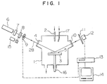
- Fig. 1 is a schematic view of an apparatus for monitoring a growing oxide superconducting film according to the present invention.
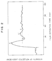
- Fig. 2 is a diagram showing changes in the intensity of reflected laser beam detected in Example 1 according to the present invention.
- Fig. 3 is a diagram showing changes in the intensity of reflected laser beam detected in Example 2 according to the present invention.
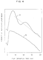
- Fig. 4 is a diagram showing changes in the intensity of reflected laser beam detected in Example 3 according to the present invention.
- Fig. 5 is a diagram showing flatness or smoothness of thin films obtained in Example 4 according to the present invention.
- Fig. 6 is a comparative diagram between the film growth rate obtained in Example 5 according to the present invention and the actual growth rate.
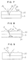
- Fig. 7 is a schematic view showing optical paths when a film growing on a substrate is irradiated with a laser beam.
- Fig. 8 is a schematic view showing optical paths when a p-polarized laser beam is irradiated at the Brewster angle of a substrate.
- Fig. 9 is a schematic view showing optical paths when p-polarized laser beam is irradiated at the Brewster angle of a film material.
- Fig. 7 is a schematic view of optical paths when a thin film growing on a substrate is irradiated with a laser beam, where numeral 5 is a substrate, 20 a growing oxide superconducting thin film, 25 a laser beam, 26 a reflected laser beam from the film surface, and 27 a reflected laser beam from the substrate surface.
- numeral 5 is a substrate
- 20 a growing oxide superconducting thin film
- 25 a laser beam
- 26 a reflected laser beam from the film surface
- 27 a reflected laser beam from the substrate surface.
- the phase difference ⁇ increases, and when ⁇ takes 2 ⁇ multiplied by an integral number, the intensity of reflected laser beam will be a maximum due to an interference, whereas it will be a minimum when ⁇ is deviated therefrom by ⁇ .
- the intensity of reflected laser beam oscillates at definite cycles corresponding to the film growth rate.
- the film thickness when the intensity of reflected laser beam is a maximum or a minimum, is proportional to 1/4 of the wavelength of a laser beam, as is obvious from the equation (1).
- Changes in the intensity of reflected laser beam can be likewise analyzed, irrespective of the wavelength, incident angle, etc. of laser beam except for special cases.
- One example of the special cases is a case that a p-polarized laser beam is led to the film or the substrate at their respective Brewster angles, where changes in the intensity of reflected laser beam are widely different from those of the foregoing cases.
- Fig. 8 is a schematic view showing optical paths when a p-polarized laser beam is led to the thin film at the Brewster angle of the substrate, where numeral 21 is the p-polarized laser beam and 22 the Brewster angle. That is, Fig. 8 shows a case where the p-polarized laser beam 21 is led to the substrate 20 at the Brewster angle 22. In that case, there is no reflection from the lower surface of growing oxide superconducting thin film 20 and the reflected laser beam to be detected is only that from the upper surface of the growing thin film.
- the flatness or smoothness of the thin film can be monitored substantially in real time from changes in the intensity of reflected p-polarized laser beam, and likewise the film thickness and the growth rate of growing thin film can be monitored from changes in the intensity of reflected s-polarized laser beam.
- Fig. 9 is a schematic view showing an optical path when a p-polarized laser beam is led to the film at the Brewster angle of the thin film material. Substantially the same results can be obtained also when the p-polarized laser beam 21 is led thereto at the Brewster angle 23 of the growing oxide superconducting thin film, except for the following difference from the case of irradiation at the Brewster angle of the substrate as shown in Fig. 8. That is, in this case, substantially no reflection takes place on the upper surface of the growing oxide superconducting thin film, and the reflected laser beam from the interface between the thin film and the substrate is dominant.
- Fig. 1 is a schematic view showing an apparatus for monitoring a growing oxide superconducting thin film according to the present invention, where numeral 1 is a reactor chamber, 2 a source gas supply nozzle, 3 a heater, 4 a laser inlet window, 5 a substrate, 6 a laser emitter, 7 a polarizer, 8 a 1/2 waveplate, 9 a chopper, 10 a laser outlet window, 11 an iris diaphragm, 12 a detector, 13 a lock-in amplifier, 14 a computer, 15 a monitor, 16 a support rotor, and 17 a gas inlet nozzle.
- numeral 1 is a reactor chamber, 2 a source gas supply nozzle, 3 a heater, 4 a laser inlet window, 5 a substrate, 6 a laser emitter, 7 a polarizer, 8 a 1/2 waveplate, 9 a chopper, 10 a laser outlet window, 11 an iris diaphragm, 12 a detector, 13 a lock-in amplifier, 14 a computer,
- a heater 3 for working on the substrate 5 is provided at a position near a source gas supply nozzle 2 in the reactor chamber 1, so that the substrate 5 can be placed on the heater 3.
- the laser emitter 6 is so arranged that the substrate 5 can be irradiated with the laser beam 28 through the laser inlet window 4 of the reactor chamber 1.
- the polarizer 7, the 1/2 waveplate 8 and the chopper 9 are provided on the optical path in this order between the laser emitter 6 and the laser inlet window 4.
- the laser beam 28 reflected from the substrate 5 is passed through the laser outlet window 10.
- the iris diaphragm 11 for cutting a room light and the silicon diode detector 12 are provided on the optical path after the laser outlet window 10, and an output from the silicon diode detector is led to a computer 14 through a lock-in amplifier 13.
- the 1/2 waveplate 8 can be rotated by a motor 15, whereby the polarization plane of laser beam can be shifted as desired.
- the heater 3 is placed on a support rotor 16, which can be horizontally moved to adjust the incident angle of the laser beam and also to rotate the substrate 5.
- a process for forming an oxide superconducting thin film will be explained below.
- a YBa2Cu3Ox film was formed on a MgO (100) single crystal substrate (single side mirror).
- Conditions for the film formation are as follows.
- ⁇ -diketone complexes i.e. Y(thd)3, Ba(thd)2, and Cu(thd)2 were used, where thd means 2,2,6,6-tetramethyl-3,5-heptanedione.
- Heating temperatures for the respective source materials were 117°C, 225°C and 101°C in that order, and flow rates of the respective carrier gases (N2) were 44, 50 and 44 cc/min, while 600 cc/min of O2 was supplied into the reactor chamber 1 through another gas inlet nozzle 17. Pressure during the film growth in the reactor chamber 1 was 8 hPa (6.0 Torr), the substrate temperature 750°C and film deposition time 2 hours.
- a He-Ne laser (wavelength: 632.8 nm) and an Ar laser (wavelength: 514.5 nm and 457.9 nm) were used, while the intensity of all the laser beams was set to 15 mW. All the laser beams 28 had a diameter of 2 mm.
- the laser beam was irradiated onto the substrate before the start to form a thin film, and recording of the intensity of the reflected laser beam was started. At the same time when the thin film formation was ended, the detection was ended. After the end of the thin film formation, the thin film was cooled in an O2 atmosphere under 1013 hPa (1 atm).
- the intensity of reflected laser beam was detected under detection conditions given in the following Examples while forming a YBa2Cu3Ox film under the above-mentioned film-forming conditions.
- the growth rate of the YBa2Cu3Ox film actually prepared was 0.30 ⁇ m/h, which was substantially in good agreement with the calculated ones. It was found from surface pictures of the film that the film surface was substantially flat and smooth.
- the base line (dashed line) of the intensity curve as shown in Fig. 2 which was obtained by eliminating the oscillatory components in the time dependence of the reflective intensity, was parallel to the abscissa.
- a s-polarized He-Ne laser beam was irradiated onto the growing thin film at an incident angle of 78° in the same manner as in Example 1, and the results of the detected intensity of reflected laser beam are shown in Fig. 3.
- deposition or precipitation of a large number of grains was observed on the film surface. It can be seen from the intensity of reflected laser beam shown in Fig. 3 that its absolute value 3 were abruptly lowered due to influences of scattering of laser beam by the grains. As a result of the scattering of the laser beam by the grains, the peak positions of Fig. 3 were expected to deviate from the actual positions. To adjust the deviations, tangents in parallel to a base line (dashed line) were drawn to obtain accurate peak positions.
- the peak positions were 18.7 min., 54.3 min. and 70.9 min. before the adjustment, whereas as a result of the adjustment the peak positions were corrected to 24.2 min., 50.5 min. and 78.4 min. respectively, and the corrected peak positions were substantially at equal distances therebetween.
- the film growth rate obtained from these values was 0.17 ⁇ m/h, which was substantially in good agreement with the actual growth rate of 0.14 ⁇ m/h.
- the base line of the intensity of reflected laser beam will have some inclination.
- the above-mentioned adjustment must be made to calculate the film thickness or growth rate from the peak positions.
- the intensity of reflected laser beam was measured by changing the polarization plane of a He-Ne laser beam alternately to 0° or 90° (i.e. p-polarized laser beam or s-polarized laser beam) at every 2 seconds by the 1/2 waveplate shown in Fig. 1.
- the incident angle of laser beam was adjusted to satisfy the conditions of Fig. 8.
- the results are shown in Fig. 4, where numeral 18 is a curve showing changes in the intensity of reflected s-polarized laser beam and 19 is a curve showing changes in the intensity of reflected p-polarized laser beam.
- a large number of grain precipitates were observed on the film surface, as in Example 2.
- the curve 19 showing the changes in the intensity of reflected p-polarized laser beam directly correspond to fluctuations of the base line, and thus more accurate peak positions can be determined and the film growth rate can be calculated therefrom.
- the film growth rate obtained from the intensity of the reflected laser beam was 0.20 ⁇ m/h, whereas the actual film growth rate was 0.18 ⁇ m/h.
- Thin films having higher Cu contents were formed by changing the heating temperature of Cu (thd)2 source material, and tested, where changes in the intensity of reflected p-polarized laser beam were measured.
- As the laser beam a He-Ne laser beam was used and the incident angle of the laser beam onto the MgO substrate in the film growth process was adjusted to the Brewster angle of MgO. A ratio of [Y]/[Ba] of the film was kept constant at 1/2.
- the curve showing changes in the reflected laser beam was approximated by a straight line and the inclination of the straight line was plotted against Cu molar ratios of the thin films (where the Ba content was fixed to 2). The results are shown in Fig. 5. From pictures of film surfaces, it was found that the amount of precipitated grains (mainly of CuO) increased with increasing Cu content. The inclination of the curve showing the changes in the intensity of reflected laser beam was decreased correspondingly, as is apparent from Fig. 5.
- MgO was used as a substrate material. Not only MgO, but also various substrate materials such as SrTiO3, LaAlO3, LaGaO3, Al2O3, Si, SiO2, NdGaO3, yttrium-stabilized zironia, etc. can be used for the same detection as above.
- Example 4 Most of single crystal substrates composed of the above-mentioned materials are transparent, whereas polycrystalline substrates of the same materials as mentioned above and various metal substrates are opaque. Thus, even if the p-polarized laser beam is led thereto at the Brewster angle, no such measurement as in Example 4 can be carried out. In that case, substantially similar results can be obtained by irradiation of the p-polarized laser beam at the Brewster angle of the film in place of the Brewster angle of the substrate. Furthermore, similar results can be obtained by making the incident angle of the laser beam equal to the Brewster angle of the film in Examples 3 and 4.
- the shape and the configuration can be determined by rotating the substrate within the substrate plane during the deposition process. Furthermore, when the thin film itself has an optical anisotropy, the crystal orientation of the thin film can be determined by rotating the substrate likewise.
- the present invention can be also used.
- the present invention can be utilized to control film forming conditions successively.
- measurement can be carried out in non-contact and non-destructive states, using a laser beam, and thus the present invention can be applied to film-forming apparatuses of any structure, so long as there are ports of leading a laser beam onto the film surface and taking out the reflected laser beam therefrom, respectively.
- the present invention can be applied to film formation not only by CVD, but also by PVD such as magnetron sputtering, laser sputtering, MBE, etc.
- any of ultraviolet light, visible light and infrared light can be used as a laser beam in the present invention and thus the light species can be selected in view of the desired species of oxide superconducting thin films, desired species of substrate, desired procedure for measurement, etc.
- the irradiation intensity of the laser beam is selected in view of the sensitivity of a detector for reflected laser beam and loss on the laser optical path, and can be increased within such a limit as not to deteriorate the film properties by the irradiation.
- a chopper can be provided on the laser optical path, and the detector outputs can be measured by a lock-in amplifier synchronized with the chopper.
- the thickness, growth rate and flatness or smoothness of a growing thin film in the growth process can be readily monitored.
- a laser beam having a low intensity can be used, and thus the detection can be carried out without deteriorating the film properties.
- the growth rate of the growing thin film can be detected, and thus a quick response to fluctuations in the growth rate, if any, can be made and occurrence of second phase precipitates or particles can be monitored and furthermore the film-forming conditions can be properly controlled.
Landscapes
- Engineering & Computer Science (AREA)
- Manufacturing & Machinery (AREA)
- Length Measuring Devices By Optical Means (AREA)
- Chemical Vapour Deposition (AREA)
- Crystals, And After-Treatments Of Crystals (AREA)
- Superconductor Devices And Manufacturing Methods Thereof (AREA)
Applications Claiming Priority (2)
| Application Number | Priority Date | Filing Date | Title |
|---|---|---|---|
| JP315089/91 | 1991-11-29 | ||
| JP3315089A JPH05149720A (ja) | 1991-11-29 | 1991-11-29 | 酸化物超電導膜の検査方法および検査装置 |
Publications (1)
| Publication Number | Publication Date |
|---|---|
| EP0545302A1 true EP0545302A1 (de) | 1993-06-09 |
Family
ID=18061278
Family Applications (1)
| Application Number | Title | Priority Date | Filing Date |
|---|---|---|---|
| EP92120284A Withdrawn EP0545302A1 (de) | 1991-11-29 | 1992-11-27 | Verfahren und Apparat zur Überwachung oxidisch supraleitender Schichten |
Country Status (2)
| Country | Link |
|---|---|
| EP (1) | EP0545302A1 (de) |
| JP (1) | JPH05149720A (de) |
Cited By (3)
| Publication number | Priority date | Publication date | Assignee | Title |
|---|---|---|---|---|
| CN110726682A (zh) * | 2019-09-26 | 2020-01-24 | 山东大学 | 一种原位在线反射光学测量系统及方法 |
| CN115807219A (zh) * | 2023-02-13 | 2023-03-17 | 南昌大学 | 一种光电薄膜材料制备控制系统及方法 |
| CN116698891A (zh) * | 2022-12-13 | 2023-09-05 | 费勉仪器科技(上海)有限公司 | 高能电子衍射测量方法及分子束外延系统 |
Families Citing this family (9)
| Publication number | Priority date | Publication date | Assignee | Title |
|---|---|---|---|---|
| US5555474A (en) * | 1994-12-21 | 1996-09-10 | Integrated Process Equipment Corp. | Automatic rejection of diffraction effects in thin film metrology |
| JP3764794B2 (ja) * | 1997-03-06 | 2006-04-12 | 松下電器産業株式会社 | 多層薄膜の膜厚測定方法と光学情報記録媒体の製造方法及び製造装置 |
| CN1302310C (zh) * | 2003-08-21 | 2007-02-28 | 中国科学院物理研究所 | 原位实时探测薄膜生长状况的光反射差装置和方法 |
| CN103644851A (zh) * | 2013-11-22 | 2014-03-19 | 大连日佳电子有限公司 | 一种在线厚度监控仪及在线厚度监控方法 |
| JP7197999B2 (ja) * | 2018-05-11 | 2022-12-28 | キオクシア株式会社 | 研磨装置および研磨パッド |
| CN110986801A (zh) * | 2019-11-15 | 2020-04-10 | 富泰华精密电子(郑州)有限公司 | 检测装置、检测设备及检测方法 |
| JP7523318B2 (ja) | 2020-03-10 | 2024-07-26 | 東京エレクトロン株式会社 | 膜厚測定装置および膜厚測定方法、ならびに成膜システムおよび成膜方法 |
| JP7616898B2 (ja) | 2021-02-17 | 2025-01-17 | 東京エレクトロン株式会社 | 膜厚測定装置、成膜システム及び膜厚測定方法 |
| JP2023009410A (ja) | 2021-07-07 | 2023-01-20 | 東京エレクトロン株式会社 | 膜厚測定方法、膜厚測定装置、および成膜システム |
Citations (2)
| Publication number | Priority date | Publication date | Assignee | Title |
|---|---|---|---|---|
| EP0426570A2 (de) * | 1989-10-31 | 1991-05-08 | Sumitomo Electric Industries, Ltd. | Verfahren und System zur Herstellung einer supraleitenden Dünnschicht aus Oxyd |
| EP0484879A2 (de) * | 1990-11-05 | 1992-05-13 | Nihon Shinku Gijutsu Kabushiki Kaisha | Gassyntheseverfahren und -vorrichtung |
-
1991
- 1991-11-29 JP JP3315089A patent/JPH05149720A/ja active Pending
-
1992
- 1992-11-27 EP EP92120284A patent/EP0545302A1/de not_active Withdrawn
Patent Citations (2)
| Publication number | Priority date | Publication date | Assignee | Title |
|---|---|---|---|---|
| EP0426570A2 (de) * | 1989-10-31 | 1991-05-08 | Sumitomo Electric Industries, Ltd. | Verfahren und System zur Herstellung einer supraleitenden Dünnschicht aus Oxyd |
| EP0484879A2 (de) * | 1990-11-05 | 1992-05-13 | Nihon Shinku Gijutsu Kabushiki Kaisha | Gassyntheseverfahren und -vorrichtung |
Non-Patent Citations (2)
| Title |
|---|
| JOURNAL OF VACUUM SCIENCE & TECHNOLOGY B vol. 7, no. 2, March 1989, NEW YORK, US pages 319 - 323 ECKSTEIN J.N. ET AL 'Epitaxial growth of high-temperature superconducting thin films' * |
| SOLID STATE COMMUNICATIONS vol. 77, no. 9, March 1991, NEW YORK, US pages 683 - 687 HABERMEIER H.U. 'The growth of (110) Y-Ba-Cu-O Thin Films and their Characterization by Optical Methods' * |
Cited By (4)
| Publication number | Priority date | Publication date | Assignee | Title |
|---|---|---|---|---|
| CN110726682A (zh) * | 2019-09-26 | 2020-01-24 | 山东大学 | 一种原位在线反射光学测量系统及方法 |
| CN116698891A (zh) * | 2022-12-13 | 2023-09-05 | 费勉仪器科技(上海)有限公司 | 高能电子衍射测量方法及分子束外延系统 |
| CN115807219A (zh) * | 2023-02-13 | 2023-03-17 | 南昌大学 | 一种光电薄膜材料制备控制系统及方法 |
| CN115807219B (zh) * | 2023-02-13 | 2023-05-30 | 南昌大学 | 一种光电薄膜材料制备控制系统及方法 |
Also Published As
| Publication number | Publication date |
|---|---|
| JPH05149720A (ja) | 1993-06-15 |
Similar Documents
| Publication | Publication Date | Title |
|---|---|---|
| US5313044A (en) | Method and apparatus for real-time wafer temperature and thin film growth measurement and control in a lamp-heated rapid thermal processor | |
| Jellison et al. | Spectroscopic ellipsometry of thin film and bulk anatase (TiO2) | |
| Jellison Jr et al. | Optical functions of silicon at elevated temperatures | |
| US5568978A (en) | Optical apparatus and method for measuring temperature of a substrate material with a temperature dependent band gap | |
| Khoshman et al. | Optical constants and band edge of amorphous zinc oxide thin films | |
| EP0545302A1 (de) | Verfahren und Apparat zur Überwachung oxidisch supraleitender Schichten | |
| Ritter et al. | Influence of substrate temperature on the condensation of vacuum evaporated films of MgF 2 and ZnS | |
| Acher et al. | I n situ investigation of the low‐pressure metalorganic chemical vapor deposition of lattice‐mismatched semiconductors using reflectance anisotropy measurements | |
| Remillard et al. | Optical studies of PdO thin films | |
| Irvine et al. | Complete in situ laser monitoring of MOCVD HgCdTe/CdTe/ZnTe growth onto GaAs substrates | |
| Svitashev et al. | Ellipsometry as a powerful tool for the control of epitaxial semiconductor structures in-situ and ex-situ | |
| Johnson et al. | Effect of substrate thickness, back surface texture, reflectivity, and thin film interference on optical band-gap thermometry | |
| Roth et al. | In situ substrate temperature measurement during MBE by band-edge reflection spectroscopy | |
| Atkinson et al. | Optical constants of thin film bismuth | |
| De Lyon et al. | Substrate temperature measurement by absorption-edge spectroscopy during molecular beam epitaxy of narrow-band gap semiconductor films | |
| Maracas et al. | Ellipsometry for III–V epitaxial growth diagnostics | |
| JPS5948786B2 (ja) | 分子線結晶成長方法 | |
| Rafla-Yuan et al. | Noncontact method for measuring coefficient of linear thermal expansion of thin films | |
| Godlewski et al. | Asymmetries in the optical properties of vacuum-deposited organic films illuminated at the substrate and non-substrate surfaces | |
| Gibbons et al. | Real-time spectroscopic ellipsometry as a characterization tool for oxide molecular beam epitaxy | |
| Duncan et al. | Real-time diagnostics of II–VI molecular beam epitaxy by spectral ellipsometry | |
| Wild et al. | Polycrystalline diamond films for optical applications | |
| Merkt et al. | The optical constants of pure and CO-covered copper films | |
| Edwards et al. | In-situ and ex-situ characterization of GaAs/AlAs quantum well structures using spectroscopic ellipsometry | |
| Hoffmann et al. | A high precision ATR study of surface plasmon mediated reflectance in noble metal films |
Legal Events
| Date | Code | Title | Description |
|---|---|---|---|
| PUAI | Public reference made under article 153(3) epc to a published international application that has entered the european phase |
Free format text: ORIGINAL CODE: 0009012 |
|
| AK | Designated contracting states |
Kind code of ref document: A1 Designated state(s): DE FR GB |
|
| 17P | Request for examination filed |
Effective date: 19930423 |
|
| 17Q | First examination report despatched |
Effective date: 19941230 |
|
| STAA | Information on the status of an ep patent application or granted ep patent |
Free format text: STATUS: THE APPLICATION HAS BEEN WITHDRAWN |
|
| 18W | Application withdrawn |
Withdrawal date: 19950707 |