EP0484879A2 - Gassyntheseverfahren und -vorrichtung - Google Patents
Gassyntheseverfahren und -vorrichtung Download PDFInfo
- Publication number
- EP0484879A2 EP0484879A2 EP91118835A EP91118835A EP0484879A2 EP 0484879 A2 EP0484879 A2 EP 0484879A2 EP 91118835 A EP91118835 A EP 91118835A EP 91118835 A EP91118835 A EP 91118835A EP 0484879 A2 EP0484879 A2 EP 0484879A2
- Authority
- EP
- European Patent Office
- Prior art keywords
- light
- film
- density
- nucleation
- substrate
- Prior art date
- Legal status (The legal status is an assumption and is not a legal conclusion. Google has not performed a legal analysis and makes no representation as to the accuracy of the status listed.)
- Granted
Links
- 230000015572 biosynthetic process Effects 0.000 title claims abstract description 51
- 238000000034 method Methods 0.000 title claims abstract description 30
- 238000003786 synthesis reaction Methods 0.000 title claims abstract description 21
- 230000006911 nucleation Effects 0.000 claims abstract description 62
- 238000010899 nucleation Methods 0.000 claims abstract description 62
- 239000000758 substrate Substances 0.000 claims abstract description 58
- 230000002194 synthesizing effect Effects 0.000 claims abstract description 53
- 238000012545 processing Methods 0.000 claims abstract description 12
- 238000000572 ellipsometry Methods 0.000 claims abstract description 8
- 230000003287 optical effect Effects 0.000 claims abstract description 6
- 229910003460 diamond Inorganic materials 0.000 claims description 38
- 239000010432 diamond Substances 0.000 claims description 38
- 239000000498 cooling water Substances 0.000 claims description 9
- 238000001816 cooling Methods 0.000 claims description 8
- 239000000463 material Substances 0.000 claims description 5
- 239000010408 film Substances 0.000 description 66
- 239000007789 gas Substances 0.000 description 27
- 230000001276 controlling effect Effects 0.000 description 9
- 238000007599 discharging Methods 0.000 description 8
- 238000004364 calculation method Methods 0.000 description 7
- 239000013078 crystal Substances 0.000 description 7
- 230000010287 polarization Effects 0.000 description 6
- 239000010409 thin film Substances 0.000 description 6
- 238000004519 manufacturing process Methods 0.000 description 5
- 230000001105 regulatory effect Effects 0.000 description 5
- XUIMIQQOPSSXEZ-UHFFFAOYSA-N Silicon Chemical compound [Si] XUIMIQQOPSSXEZ-UHFFFAOYSA-N 0.000 description 4
- 238000011156 evaluation Methods 0.000 description 4
- 238000005259 measurement Methods 0.000 description 4
- VNWKTOKETHGBQD-UHFFFAOYSA-N methane Chemical compound C VNWKTOKETHGBQD-UHFFFAOYSA-N 0.000 description 4
- 239000000843 powder Substances 0.000 description 4
- 229910052710 silicon Inorganic materials 0.000 description 4
- 239000010703 silicon Substances 0.000 description 4
- 238000004891 communication Methods 0.000 description 3
- 238000012544 monitoring process Methods 0.000 description 3
- 238000006748 scratching Methods 0.000 description 3
- 230000002393 scratching effect Effects 0.000 description 3
- 239000002356 single layer Substances 0.000 description 3
- UFHFLCQGNIYNRP-UHFFFAOYSA-N Hydrogen Chemical compound [H][H] UFHFLCQGNIYNRP-UHFFFAOYSA-N 0.000 description 2
- 230000008901 benefit Effects 0.000 description 2
- 230000008859 change Effects 0.000 description 2
- 238000007796 conventional method Methods 0.000 description 2
- 238000010586 diagram Methods 0.000 description 2
- 239000001257 hydrogen Substances 0.000 description 2
- 229910052739 hydrogen Inorganic materials 0.000 description 2
- 239000010410 layer Substances 0.000 description 2
- 244000144985 peep Species 0.000 description 2
- 239000004065 semiconductor Substances 0.000 description 2
- 239000004215 Carbon black (E152) Substances 0.000 description 1
- 238000004458 analytical method Methods 0.000 description 1
- 238000013459 approach Methods 0.000 description 1
- 238000006243 chemical reaction Methods 0.000 description 1
- 239000011248 coating agent Substances 0.000 description 1
- 238000000576 coating method Methods 0.000 description 1
- 229930195733 hydrocarbon Natural products 0.000 description 1
- 150000002430 hydrocarbons Chemical class 0.000 description 1
- 238000012986 modification Methods 0.000 description 1
- 230000004048 modification Effects 0.000 description 1
- 230000000149 penetrating effect Effects 0.000 description 1
- 230000008569 process Effects 0.000 description 1
- 230000004044 response Effects 0.000 description 1
- 238000004088 simulation Methods 0.000 description 1
- 238000011144 upstream manufacturing Methods 0.000 description 1
Images


Classifications
-
- C—CHEMISTRY; METALLURGY
- C30—CRYSTAL GROWTH
- C30B—SINGLE-CRYSTAL GROWTH; UNIDIRECTIONAL SOLIDIFICATION OF EUTECTIC MATERIAL OR UNIDIRECTIONAL DEMIXING OF EUTECTOID MATERIAL; REFINING BY ZONE-MELTING OF MATERIAL; PRODUCTION OF A HOMOGENEOUS POLYCRYSTALLINE MATERIAL WITH DEFINED STRUCTURE; SINGLE CRYSTALS OR HOMOGENEOUS POLYCRYSTALLINE MATERIAL WITH DEFINED STRUCTURE; AFTER-TREATMENT OF SINGLE CRYSTALS OR A HOMOGENEOUS POLYCRYSTALLINE MATERIAL WITH DEFINED STRUCTURE; APPARATUS THEREFOR
- C30B25/00—Single-crystal growth by chemical reaction of reactive gases, e.g. chemical vapour-deposition growth
- C30B25/02—Epitaxial-layer growth
-
- C—CHEMISTRY; METALLURGY
- C30—CRYSTAL GROWTH
- C30B—SINGLE-CRYSTAL GROWTH; UNIDIRECTIONAL SOLIDIFICATION OF EUTECTIC MATERIAL OR UNIDIRECTIONAL DEMIXING OF EUTECTOID MATERIAL; REFINING BY ZONE-MELTING OF MATERIAL; PRODUCTION OF A HOMOGENEOUS POLYCRYSTALLINE MATERIAL WITH DEFINED STRUCTURE; SINGLE CRYSTALS OR HOMOGENEOUS POLYCRYSTALLINE MATERIAL WITH DEFINED STRUCTURE; AFTER-TREATMENT OF SINGLE CRYSTALS OR A HOMOGENEOUS POLYCRYSTALLINE MATERIAL WITH DEFINED STRUCTURE; APPARATUS THEREFOR
- C30B25/00—Single-crystal growth by chemical reaction of reactive gases, e.g. chemical vapour-deposition growth
- C30B25/02—Epitaxial-layer growth
- C30B25/16—Controlling or regulating
-
- C—CHEMISTRY; METALLURGY
- C30—CRYSTAL GROWTH
- C30B—SINGLE-CRYSTAL GROWTH; UNIDIRECTIONAL SOLIDIFICATION OF EUTECTIC MATERIAL OR UNIDIRECTIONAL DEMIXING OF EUTECTOID MATERIAL; REFINING BY ZONE-MELTING OF MATERIAL; PRODUCTION OF A HOMOGENEOUS POLYCRYSTALLINE MATERIAL WITH DEFINED STRUCTURE; SINGLE CRYSTALS OR HOMOGENEOUS POLYCRYSTALLINE MATERIAL WITH DEFINED STRUCTURE; AFTER-TREATMENT OF SINGLE CRYSTALS OR A HOMOGENEOUS POLYCRYSTALLINE MATERIAL WITH DEFINED STRUCTURE; APPARATUS THEREFOR
- C30B25/00—Single-crystal growth by chemical reaction of reactive gases, e.g. chemical vapour-deposition growth
- C30B25/02—Epitaxial-layer growth
- C30B25/16—Controlling or regulating
- C30B25/165—Controlling or regulating the flow of the reactive gases
-
- G—PHYSICS
- G01—MEASURING; TESTING
- G01N—INVESTIGATING OR ANALYSING MATERIALS BY DETERMINING THEIR CHEMICAL OR PHYSICAL PROPERTIES
- G01N21/00—Investigating or analysing materials by the use of optical means, i.e. using sub-millimetre waves, infrared, visible or ultraviolet light
- G01N21/17—Systems in which incident light is modified in accordance with the properties of the material investigated
- G01N21/21—Polarisation-affecting properties
- G01N21/211—Ellipsometry
Definitions
- This invention relates to a method and apparatus for gas phase synthesis and, in particular, to a method of synthesizing in gas phase a functional material or a hard film, especially a diamond film to be used for mechanical purposes and for semiconductor purposes, as well as to an apparatus for carrying out this method.
- the adhesion of the film to a substrate is an important matter of interest. This matter is known to be solved by controlling or increasing the density of nucleation of the diamond crystal nuclei grown at the beginning on the substrate.
- the diamond film is used as a protection film on an optical window or a protection film of a lens
- the surface of the diamond film formed cannot be made smooth if the density of the nucleation is small. Therefore, in this case, it is also necessary to control or increase the density of nucleation of the diamond crystal nuclei.
- the diamond film is used for semiconductor purposes, it is necessary to epitaxilly grow the diamond film.
- the film be formed under conditions of high density of growth of crystal nuclei, i.e., high density of nucleation.
- controlling or increasing the density of nucleation is especially important in utilizing the material susceptible of easy nucleus growth such as diamond as a functional material or as a hard film.
- This method of scratching treatment with diamond powders is a method in which prior to film formation a substrate is placed into a solution containing therein diamond powders outside a synthesizing apparatus and subject it to ultrasonic vibrations for a predetermined period of time, or the substrate is rubbed against diamond powders to form very fine scratches on the substrate. Thereafter, the film is formed on the substrate.
- the density of the scratches to be formed on the substrate the density of nucleation can be controlled to a certain degree within a range of 105 to 109/cm2.
- the evaluation of the density of nucleation of the diamond nuclei has generally been made by taking out a sample, after film formation, to examine with an electron microscope or the like, thereby counting the number of grown nuclei within a predetermined area.
- the electron microscope in case the number of grown nuclei is counted in process with an electron microscope, the electron microscope must be placed inside an apparatus for gas phase synthesis. It is impossible to count the number in such a high-pressure zone as in the method of gas phase synthesis because the means free path of the electrons is short.
- this invention has an object of providing a method of gas phase synthesis in which exact control of the density of nucleation can be carried out, as well as an instrument for carrying out the method.
- the gas phase synthesizing method according to this invention is characterize by the steps of measuring, by ellipsometry, optical properties of a surface of a sample on which a film is formed during formation of the film, and of evaluating the density of nucleation from changes in ellipsometric parameter angles during forming of the film .
- the density of nucleation is controlled by adjusting a temperature of the substrate.
- the material to be synthesized is, for example, diamond.
- the gas phase synthesizing apparatus comprises a synthesizing chamber, a light source means which is disposed outside the synthesizing chamber for radiating polarized light into the synthesizing chamber, a light-inlet window mounted on said synthesizing chamber for introducing thereinto the light radiated from the light source means, a light-outlet window mounted on the synthesizing chamber for leading the light introduced from the light-inlet window and reflected from a substrate on which a film is being formed out of the synthesizing chamber, a light-receiving means for receiving the light reflected from the substrate and passed through the light-outlet window, and a data processing system for receiving an output signal from said light-receiving means for determining the density of nucleation.
- the synthesizing chamber may further comprise a vacuum exhausting system connected thereto, a substrate electrode having a cooling circuit for maintaining the substrate to a predetermined temperature, and flow rate control means provided in the cooling circuit for adjusting an amount of cooling water through said cooling circuit.
- the flow rate control means may be communicated with the data processing system.
- the polarized light such as laser light or the like is irradiated to the sample during the formation of the film to measure the changes in polarization before and after the reflection of the light on the film.
- These changes in the polarized light are representative of the optical or geometrical conditions of the surface of the sample. Since the differences in the density of nucleation appear as the differences in the geometrical shapes on the surface of the sample, it becomes possible to evaluate the density of nucleation by ellipsometry.
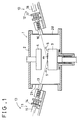
- Fig. 1 is an example of an apparatus for carrying out this invention method of gas phase synthesizing.
- Numeral 1 denotes an apparatus for gas phase synthesis.
- This gas phase synthesizing apparatus 1 comprises a synthesizing chamber 2 for carrying out synthesizing therein. Inside this synthesizing chamber 2, a substrate electrode 3 is rotatably provided at a lower portion thereof and a discharging electrode 4 is provided at an upper portion thereof. In the neighborhood of the substrate electrode 3, there is provided a ring-like pipe 5 for introducing a reactive gas for diamond synthesis.
- the gas phase synthesizing apparatus 1 is provided with an ellipsometer 10 for evaluating the density of nucleation of diamond crystal nuclei to be formed on a substrate m.
- This ellipsometer 10 is provided with a light source system 11 and a light receiving system 12.
- the light source system 11 comprises a light incident window 14, to function as a peep hole, which is provided in communication with an opening 13 which is formed in a side wall 2a of the synthesizing chamber 2, and a light source member 15 for emitting polarized laser light or the like for analyzing the surface of the substrate m.
- the light receiving system 12 comprises: a light emitting window 17, to function as a peep hole, which is provided in communication with an opening 16 which is located in a side wall 2b of the synthesizing chamber 2 at a position diametrically opposite to the side wall 2a and is formed on an optical axis of the light reflected from the substrate m; and a light receiving member 18 to receive the reflected light.
- the light receiving member 18 is connected to a data processing system for measuring and analyzing the changes in the polarization state of the light before and after reflection on the surface of the substrate m.
- the ellipsometric simulating calculation can be performed as follows.
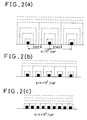
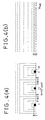
- the grown diamond is in the form of nuclei, if the wave length of the light to be measured is in the length of several times the distance between the nuclei, an effective medium approximate calculation can be applied; the grown diamond can be treated in the same way as a homogeneous film.
- N is the density of nucleation
- n is the refractive index of the bulk diamond
- D is the length of one side of each diamond nucleus of cubic shape
- the effective refractive index n eff of a homogeneous film having a thickness of D can be expressed by the following formula (see Fig. 4(a) and (b)):
- r 1p and r 2p are Fresnel reflection coefficients of components p of polarized light
- r 1s and r 2s are Fresnel reflection coefficients of components s of polarized light
- r 1p and r 1s are Fresnel coefficients between vacuum and the equivalent single-layer film
- r 2p and r 2s are Fresnel coefficients between the equivalent single-layer film and the substrate
- e is a base of natural logarithm
- i is ⁇ -1 ⁇
- ⁇ and ⁇ are ellipsometric parameter angles.
- d can be obtained by the following formula: where ⁇ is the wave length of the light and ⁇ is the angle of incidence.
- Fig. 5 shows another embodying example of this invention apparatus for gas phase synthesis. The difference between the apparatus as shown in Fig. 5 and the apparatus as shown in Fig. 1 is explained hereinbelow.
- the synthesizing chamber 2 is connected to an evacuating system 6 such as vacuum pumps or the like via exhausting pipes 8 which are provided with regulating valves 7.
- the light receiving member 18 is connected to a computer-equipped data processing system 19 which performs the ellipsometric analysis by analyzing the changes in polarization before and after the reflection of the light on the surface of the substrate m.
- the substrate electrode 3 is connected to a circulation pipe 20 for circulating therein cooling water for cooling the electrode 3.
- the flow rate control device 21 and the data processing system 19 are communicated with each other so that the flow rate adjustment of the cooling water in the circulation pipe 20 can be made by adjusting the opening degree of the flow rate control device 21 depending on the control voltage to be output from the data processing system 19.
- the pressure i.e., the vacuum degree inside the synthesizing chamber 2 can be maintained in a predetermined value by opening or closing the regulating valve 7. Further, even if the substrate m becomes higher in temperature due to the electric discharging during film formation, it can be cooled by circulating cooling water through the cooling pipe 20. Furthermore, by providing the circulating pipe 20 with the flow rate control device 21 which is in communication with the data processing system 19, the substrate m can be maintained at a predetermined temperature to suit the formation of the thin film having a desired density N of nucleation, even though the temperature of the substrate m may be raised due to the electric discharging during the formation of the thin film.
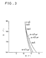
- the density of nucleation was obtained in the following manner through the changes in the ellipsometric parameter angles.
- the diamond film can be formed by synthesis on the substrate m while controlling the opening degree of the flow rate control device 21 by the control voltage which is output from the computer-equipped data processing system 19 for polarization monitoring.
- the thin diamond film having a density of nucleation of 109/cm2 or more while maintaining the substrate temperature as low as possible in each film formation operation.
- This kind of method is effective in an actual manufacturing stage. In other words, since the apparatuses become complicated and on a large scale in the manufacturing facility and, as a result, it is estimated that the accuracy of ellipsometric measurement generally becomes poor. If the accuracy of ellipsometric measurement becomes poor, the size of the diamond nuclei of minimum requirement in accurately obtaining the density of nucleation, becomes large. Then, there are cases where it is too late for the control in the batch operation which is then in progress.
- the production may be stopped at as early a stage as possible to remove the product of poor quality so that a step can be taken to change the film formation conditions of the next batch of production.
- the difference value ⁇ of the parameter angles ⁇ before and during the film formation was used in obtaining the density of nucleation.
- this method is simple, the following method may also be used to obtain a more accurate density of nucleation. Namely, there is obtained by calculation a curve which most closely approaches the curve which represents the changes in the empirically obtained ⁇ value and ⁇ value of parameter angles, i.e., a locus of points ( ⁇ , ⁇ ) of parameter angle values on the coordinates by varying parameters as the density N of nucleation, the height D of the nuclei and so on.
- the angle ⁇ and the angle ⁇ have parameters such as the density N of nucleation, the height D of the nuclei, the refractive index n s of the substrate, the refractive index n of bulk diamond, the incidence angle ⁇ , the refractive index n i of the boundary layer, and the thickness d i of the boundary layer and the like. If the nucleus height D of the nuclei is changed among these parameters, a curve can be drawn. A curve that can be naturally determined by a combination of values of parameters to be selected from among the remaining parameters, is compared with the experimental data by, e.g., a method of least squares. The N value then obtained becomes the density of nucleation.
- the film forming conditions during the film forming operation are not limited to the above-described adjustments of the substrate temperature. Instead, the concentration of hydrocarbon in the synthesis gas to be introduced into the synthesizing chamber 2, the pressure inside the synthesizing chamber 2, the discharging electric current, or the like may be set to an appropriate value in response to the density of nucleation of the diamond thin film to be formed on the substrate m.
- the synthesizing chamber 2 is connected to the evacuating pump 6 via regulating valves 7, the vacuum degree inside the synthesizing chamber 2 can be easily maintained at a desired pressure by the operation of the regulating valves.
- gas phase synthesizing apparatus of this invention it is possible to provide an apparatus in which the density of nucleation can be grasped by measuring and analyzing the polarization state of the light as reflected from the substrate to facilitate the control of the film formation of a predetermined density of nucleation and in which the diamond thin film having a very accurately controlled density of nucleation can be easily formed on the substrate.
- the synthesizing chamber with the substrate electrode which is equipped with the flow rate control device for cooling water, it becomes easy to adjust the substrate temperature during the film formation.
Landscapes
- Chemical & Material Sciences (AREA)
- Chemical Kinetics & Catalysis (AREA)
- General Chemical & Material Sciences (AREA)
- Engineering & Computer Science (AREA)
- Crystallography & Structural Chemistry (AREA)
- Materials Engineering (AREA)
- Metallurgy (AREA)
- Organic Chemistry (AREA)
- Physics & Mathematics (AREA)
- Health & Medical Sciences (AREA)
- Life Sciences & Earth Sciences (AREA)
- Analytical Chemistry (AREA)
- Biochemistry (AREA)
- General Health & Medical Sciences (AREA)
- General Physics & Mathematics (AREA)
- Immunology (AREA)
- Pathology (AREA)
- Crystals, And After-Treatments Of Crystals (AREA)
- Investigating Or Analysing Materials By Optical Means (AREA)
Applications Claiming Priority (2)
| Application Number | Priority Date | Filing Date | Title |
|---|---|---|---|
| JP297167/90 | 1990-11-05 | ||
| JP29716790 | 1990-11-05 |
Publications (3)
| Publication Number | Publication Date |
|---|---|
| EP0484879A2 true EP0484879A2 (de) | 1992-05-13 |
| EP0484879A3 EP0484879A3 (en) | 1993-03-31 |
| EP0484879B1 EP0484879B1 (de) | 1997-02-05 |
Family
ID=17843057
Family Applications (1)
| Application Number | Title | Priority Date | Filing Date |
|---|---|---|---|
| EP19910118835 Expired - Lifetime EP0484879B1 (de) | 1990-11-05 | 1991-11-05 | Gassyntheseverfahren und -vorrichtung |
Country Status (3)
| Country | Link |
|---|---|
| EP (1) | EP0484879B1 (de) |
| JP (1) | JPH05889A (de) |
| DE (1) | DE69124565T2 (de) |
Cited By (3)
| Publication number | Priority date | Publication date | Assignee | Title |
|---|---|---|---|---|
| EP0545302A1 (de) * | 1991-11-29 | 1993-06-09 | Hitachi, Ltd. | Verfahren und Apparat zur Überwachung oxidisch supraleitender Schichten |
| WO1994011722A1 (en) * | 1992-11-12 | 1994-05-26 | Santa Barbara Research Center | Reflection-free ellipsometry measurement apparatus and method for small sample cells |
| KR100946596B1 (ko) | 2008-02-28 | 2010-03-09 | 한양대학교 산학협력단 | 매핑용 타원해석기 |
Families Citing this family (2)
| Publication number | Priority date | Publication date | Assignee | Title |
|---|---|---|---|---|
| KR100352127B1 (ko) * | 2000-04-11 | 2002-09-12 | 김상열 | 회전검광자형 in situ 타원계 |
| KR20040041311A (ko) * | 2002-11-11 | 2004-05-17 | 삼성전자주식회사 | 유기 박막의 물성적 특성을 분석하기 위한 방법 및 장치 |
Family Cites Families (3)
| Publication number | Priority date | Publication date | Assignee | Title |
|---|---|---|---|---|
| US4332833A (en) * | 1980-02-29 | 1982-06-01 | Bell Telephone Laboratories, Incorporated | Method for optical monitoring in materials fabrication |
| GB8606748D0 (en) * | 1986-03-19 | 1986-04-23 | Secr Defence | Monitoring surface layer growth |
| US4906844A (en) * | 1988-08-12 | 1990-03-06 | Rockwell International Corporation | Phase sensitive optical monitor for thin film deposition |
-
1991
- 1991-10-09 JP JP91262318A patent/JPH05889A/ja active Pending
- 1991-11-05 EP EP19910118835 patent/EP0484879B1/de not_active Expired - Lifetime
- 1991-11-05 DE DE1991624565 patent/DE69124565T2/de not_active Expired - Fee Related
Cited By (3)
| Publication number | Priority date | Publication date | Assignee | Title |
|---|---|---|---|---|
| EP0545302A1 (de) * | 1991-11-29 | 1993-06-09 | Hitachi, Ltd. | Verfahren und Apparat zur Überwachung oxidisch supraleitender Schichten |
| WO1994011722A1 (en) * | 1992-11-12 | 1994-05-26 | Santa Barbara Research Center | Reflection-free ellipsometry measurement apparatus and method for small sample cells |
| KR100946596B1 (ko) | 2008-02-28 | 2010-03-09 | 한양대학교 산학협력단 | 매핑용 타원해석기 |
Also Published As
| Publication number | Publication date |
|---|---|
| DE69124565T2 (de) | 1997-09-11 |
| EP0484879B1 (de) | 1997-02-05 |
| EP0484879A3 (en) | 1993-03-31 |
| DE69124565D1 (de) | 1997-03-20 |
| JPH05889A (ja) | 1993-01-08 |
Similar Documents
| Publication | Publication Date | Title |
|---|---|---|
| Aspnes | Real-time optical diagnostics for epitaxial growth | |
| US5276503A (en) | Method and apparatus for gas phase synthesis | |
| US20050117164A1 (en) | Method and apparatus for measuring thickness of thin film and device manufacturing method using same | |
| JP2004335841A (ja) | プラズマ処理装置の予測装置及び予測方法 | |
| Callard et al. | Fabrication and characterization of graded refractive index silicon oxynitride thin films | |
| US7342225B2 (en) | Crystallographic metrology and process control | |
| EP0484879B1 (de) | Gassyntheseverfahren und -vorrichtung | |
| Giba et al. | Controlling refractive index in AlN films by texture and crystallinity manipulation | |
| Zhang et al. | Scaling behavior and structure transition of ZrO2 films deposited by RF magnetron sputtering | |
| Von Keudell et al. | Role of hydrogen ions in plasma‐enhanced chemical vapor deposition of hydrocarbon films, investigated by in situ ellipsometry | |
| US6726767B1 (en) | Layer processing | |
| Remillard et al. | Optical studies of PdO thin films | |
| Spanos et al. | Investigation of roughened silicon surfaces using fractal analysis. II. Chemical etching, rapid thermal chemical vapor deposition, and thermal oxidation | |
| Cobet et al. | Surface termination during GaN growth by metalorganic vapor phase epitaxy determined by ellipsometry | |
| JPH02124406A (ja) | 半導体製造装置 | |
| Pickering | Spectroscopic ellipsometry for monitoring and control of surfaces, thin layers and interfaces | |
| Kroesen et al. | Depth profiling of the Ge concentration in SiGe alloys using in situ ellipsometry during reactive‐ion etching | |
| Bell et al. | Real-time optical characterization of heteroepitaxy by organometallic chemical vapor deposition | |
| Kostiukevych | Transducer based on surface plasmon resonance with thermal modification of metal layer properties | |
| Zauner et al. | Spectroscopic ellipsometry on GaN: Comparison between hetero-epitaxial layers and bulk crystals | |
| Aspnes | Real-Time Surface and Near-Surface Optical Diagnostics for Epitaxial Growth | |
| EP1123562B1 (de) | Schichtbearbeitung | |
| Huerta-Ruelas et al. | Observation of thermal desorption and MBE growth rate using laser light scattering | |
| Pickering et al. | Angle-resolved light scattering studies of silicon-on-sapphire | |
| Rathnathilaka | Wafer-scale fabrication and characterisation of SiN thin films for cryoelectronic applications |
Legal Events
| Date | Code | Title | Description |
|---|---|---|---|
| PUAI | Public reference made under article 153(3) epc to a published international application that has entered the european phase |
Free format text: ORIGINAL CODE: 0009012 |
|
| AK | Designated contracting states |
Kind code of ref document: A2 Designated state(s): DE FR GB |
|
| PUAL | Search report despatched |
Free format text: ORIGINAL CODE: 0009013 |
|
| AK | Designated contracting states |
Kind code of ref document: A3 Designated state(s): DE FR GB |
|
| 17P | Request for examination filed |
Effective date: 19930826 |
|
| 17Q | First examination report despatched |
Effective date: 19950728 |
|
| GRAG | Despatch of communication of intention to grant |
Free format text: ORIGINAL CODE: EPIDOS AGRA |
|
| GRAH | Despatch of communication of intention to grant a patent |
Free format text: ORIGINAL CODE: EPIDOS IGRA |
|
| GRAH | Despatch of communication of intention to grant a patent |
Free format text: ORIGINAL CODE: EPIDOS IGRA |
|
| GRAA | (expected) grant |
Free format text: ORIGINAL CODE: 0009210 |
|
| AK | Designated contracting states |
Kind code of ref document: B1 Designated state(s): DE FR GB |
|
| REF | Corresponds to: |
Ref document number: 69124565 Country of ref document: DE Date of ref document: 19970320 |
|
| ET | Fr: translation filed | ||
| PLBE | No opposition filed within time limit |
Free format text: ORIGINAL CODE: 0009261 |
|
| STAA | Information on the status of an ep patent application or granted ep patent |
Free format text: STATUS: NO OPPOSITION FILED WITHIN TIME LIMIT |
|
| 26N | No opposition filed | ||
| PGFP | Annual fee paid to national office [announced via postgrant information from national office to epo] |
Ref country code: GB Payment date: 19981023 Year of fee payment: 8 |
|
| PGFP | Annual fee paid to national office [announced via postgrant information from national office to epo] |
Ref country code: FR Payment date: 19981127 Year of fee payment: 8 |
|
| PGFP | Annual fee paid to national office [announced via postgrant information from national office to epo] |
Ref country code: DE Payment date: 19990129 Year of fee payment: 8 |
|
| PG25 | Lapsed in a contracting state [announced via postgrant information from national office to epo] |
Ref country code: GB Free format text: LAPSE BECAUSE OF NON-PAYMENT OF DUE FEES Effective date: 19991105 |
|
| GBPC | Gb: european patent ceased through non-payment of renewal fee |
Effective date: 19991105 |
|
| PG25 | Lapsed in a contracting state [announced via postgrant information from national office to epo] |
Ref country code: FR Free format text: LAPSE BECAUSE OF NON-PAYMENT OF DUE FEES Effective date: 20000731 |
|
| PG25 | Lapsed in a contracting state [announced via postgrant information from national office to epo] |
Ref country code: DE Free format text: LAPSE BECAUSE OF NON-PAYMENT OF DUE FEES Effective date: 20000901 |
|
| REG | Reference to a national code |
Ref country code: FR Ref legal event code: ST |