EP0545544B1 - Registre à décalage optique à rebouclage linéaire - Google Patents
Registre à décalage optique à rebouclage linéaire Download PDFInfo
- Publication number
- EP0545544B1 EP0545544B1 EP92309953A EP92309953A EP0545544B1 EP 0545544 B1 EP0545544 B1 EP 0545544B1 EP 92309953 A EP92309953 A EP 92309953A EP 92309953 A EP92309953 A EP 92309953A EP 0545544 B1 EP0545544 B1 EP 0545544B1
- Authority
- EP
- European Patent Office
- Prior art keywords
- clock signal
- optical
- encoded
- output
- control
- Prior art date
- Legal status (The legal status is an assumption and is not a legal conclusion. Google has not performed a legal analysis and makes no representation as to the accuracy of the status listed.)
- Expired - Lifetime
Links
Images

Classifications
-
- G—PHYSICS
- G02—OPTICS
- G02F—OPTICAL DEVICES OR ARRANGEMENTS FOR THE CONTROL OF LIGHT BY MODIFICATION OF THE OPTICAL PROPERTIES OF THE MEDIA OF THE ELEMENTS INVOLVED THEREIN; NON-LINEAR OPTICS; FREQUENCY-CHANGING OF LIGHT; OPTICAL LOGIC ELEMENTS; OPTICAL ANALOGUE/DIGITAL CONVERTERS
- G02F3/00—Optical logic elements; Optical bistable devices
-
- G—PHYSICS
- G06—COMPUTING OR CALCULATING; COUNTING
- G06E—OPTICAL COMPUTING DEVICES
- G06E1/00—Devices for processing exclusively digital data
-
- G—PHYSICS
- G11—INFORMATION STORAGE
- G11C—STATIC STORES
- G11C21/00—Digital stores in which the information circulates continuously
-
- H—ELECTRICITY
- H03—ELECTRONIC CIRCUITRY
- H03K—PULSE TECHNIQUE
- H03K3/00—Circuits for generating electric pulses; Monostable, bistable or multistable circuits
- H03K3/84—Generating pulses having a predetermined statistical distribution of a parameter, e.g. random pulse generators
Definitions
- This invention relates to optical linear feedback shift registers.
- All-optical information processing holds promise for processing throughput rates which are much faster than electronics.
- One illustrative prior art all-optical shift register is described in US-A-4,923,267 as constructed from at least two optical memory cells connected in cascade, each memory cell having an optical combiner, a 1 X 2 optical switch, a clock, and an optical amplifier, all connected by optical fibers.
- Each memory cell in the sequence is connected to the next sequential cell by an optical fiber from its output port to the input port of the next sequential cell.
- the input port of the first optical memory cell serves as the input to the shift register.
- the output port of the last sequential optical memory cell serves as the output port of the shift register.
- Each cell is controlled by a clock, all clocks operating at the same rate, but each out of phase with the clock in the next sequential cell.
- Control signals are provided by said clocks to shift optical pulses from one cell to the next for the enter-shift-exit cycle of the shift register.
- silica optical fiber Despite its relatively weak nonlinear index, silica optical fiber remains the most promising medium for realizing all-optical processing systems. The loss is low enough that extremely long lengths can be used to compensate for the weak nonlinearity, and there is vast amount of existing technology that can be exploited in building a system. All-optical fiber Sagnac interferometer switches have been demonstrated in a number of different formats, and at extremely high speeds. Such Sagnac switches are extremely simple structures which are also immune to fluctuations in ambient conditions, and much experience has been accumulated in the development of Sagnac-based fiber optic gyroscopes.
- a control beam must be used which is isolated from a separate signal beam.
- Two distinct optical wavelengths can be used, in which case lossless combination and separation of the control and signal can be effected using wavelength dependent couplers or filters. While the use of different wavelengths is an elegant scheme for a simple system, the complexity grows as the system grows in complexity, because identical devices of this type cannot be cascaded.
- a polarization-based Sagnac switch was demonstrated, in which polarization rather than wavelength was used to distinguish the control beam from the signal beam. Stable polarization-based interferometry is achieved in a Sagnac switch by using polarizing couplers.
- an optical linear feedback shift register arrangement as claimed in claim 1.
- an optical linear feedback shift register as claimed in claim 7.
- an optical linear feedback shift register as claimed in claim 15.
- an optical linear feedback shift register arrangement is implemented using an optical encoding means.
- the encoding means encodes a received optical clock signal with a value derived from an exclusive-or of the first and second delayed versions of an encoded signal received, respectively, at first and second control ports.
- the resulting encoded clock signal, appearing at an output port, is then coupled through a first delay means to said first control port and coupled through a second delay means to said second control port.
- an optical communication system utilizes the above-described linear feedback shift register to encode a data signal at a transmitter location and uses an identical linear feedback shift register at the receiver location to decode the encoded data signal.
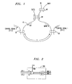
- An optical exclusive-or logic gate 100 may be implemented using a Sagnac interferometer switch arrangement 110 (hereinafter Sagnac switch) modified to include two control inputs.
- Sagnac switch is described in more detail in the co-pending United States patent application, Serial No. 07/521774 of Gabriel, Houh and Whitaker entitled “Sagnac Optical Logic Gate,” filed May 10, 1990.
- the Sagnac switch illustratively, includes an optical transmission medium, i.e., an optical fiber 10, that is connected at both ends to a coupler 20.
- An input signal is applied to an input IN, which is coupled through coupler 40, to port 1 of coupler 20.
- Coupler 40 also enables a reflected output appearing at port 1 of coupler 20 to be coupled to output OUT1.
- Ports 2 and 4 of coupler 20 are connected to the two ends of fiber 10.
- Port 3 of coupler 20 forms a second output OUT2 of the Sagnac switch.
- Fiber 10 forms a loop, (also referred to herein as fiber loop 10) which in the context of this disclosure, refers to the path over which a signal travels and, more particularly, to arrangements where the path forms a closed, or nearly closed, figure.
- the Sagnac switch operates as follows. An input signal IN applied to port 1 is split into two parts that exit coupler 20 at ports 2 and 4: a "mark” signal that travels clockwise, and a “ref” signal (reference signal) that travels counterclockwise.
- the "mark” and “ref” signals travel through the loop in opposite directions, re-enter coupler 20 and recombine therein. Under normal circumstances, the "mark” and “ref” signals experience the same conditions as they travel through the loop. Even though the propagation speed is a function of many parameters that may be uncontrollable and may or may not change with time, the travel time of the "ref" and “mark” signals is short enough that, basically, all of the parameters remain static.
- FIG. 1 includes a coupler 30 that injects a first control signal CTL1 into a segment 11 of the fiber loop 10. Because coupler 30 is within the loop, the control signal CTL1 travels along the loop only in one direction; and more specifically, coupler 30 is arranged to inject the control signal that travels along the loop in the clockwise direction of the "mark" signal. Similarly, coupler 50 injects a second control signal CTL2 into segment 11 of the fiber loop 10 in the same counter-clockwise direction as the "ref" signal.
- control pulse When a control pulse is sent into loop 10, it is timed with respect to the input generated pulse (reference or interacting pulse) so that the pulse that propagates faster is preceded by the pulse that propagates slower. While propagating through the loop, the faster pulse overtakes and completely surpasses the slower pulse, causing the two pulses to traverse each other. (It should be kept in mind that the term "traverse" is used in a bilateral sense. When pulse A traverses pulse B, pulse B also traverses pulse A.) In this manner, the control pulse affects the propagation speed of the pulse sent in the same direction through the Sagnac loop and modifies the phase of the affected pulse as it re-enters the coupler 20. When the intensity of the control pulse is properly controlled, the phase shift caused by the control pulse (on the pulse sent in the control pulse direction) is such that no reflected signal appears at the input port 1 of the coupler 20.
- Segment 11 of fiber 10 is a variable refractive-index material that is characterized by the property that the propagation speed of a light beam passing through the material is a function of the energy of the beam that passes through the material. Furthermore, not only does the propagation speed change for the beam that effects the change in propagation speed, but it also changes the propagation speed of other beams that pass through the material at the same time.
- the entire length of fiber 10 may be made of such a variable refractive-index material, but for the sake of generality, FIG. 1 is drawn with only a limited segment being made up of this material. Also for the sake of generality, it should be pointed out that the loop of fiber 10 in FIG. 1 does not necessarily have to be fiber. It can be a waveguide or other means for directing the flow of light.
- the arrangement of FIG. 1 includes a fiber loop 10 having a controllable propagation speed material in segment 11, "mark” and “ref” signals traveling through the loop in opposite directions and combined in coupler 20, a first control signal CTL1 that is injected at coupler 30 which travels in the same direction as the "mark” signal, and a second control signal CTL2 that is injected at coupler 50 and which travels in the same direction as the "ref” signal.
- the circuit of FIG. 1 provides an exclusive-or function on the control signals CTL1 and CTL2.
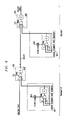
- FIG. 2 we illustrate a standard exclusive-or gate representation of our circuit of FIG. 1.
- the exclusive-or function requires that if both input signals I1 and I2 are absent (logic 0) or present (logic 1), then the output OUT is absent (logic 0). However, if either input signal I1 or I2 is present (logic 1), then the output OUT is present (logic 1).
- the circuit of FIG. 1 provides the exclusive-or function of FIG. 2 if control signal CTL1 is defined as input I1, control signal CTL2 is defined as input I2, OUT2 is the non-inverted output and OUT1 is the inverted output.
- the input IN of FIG. 1 is, illustratively, shown as the power lead of FIG. 2.
- control pulses CTL1 and CTL2 are approximately the same shape (although as discussed later only the overall energy of the control signals CTL1 and CTL2 need be the same to have the same propagation speed alteration effects).
- control signal CTL1 when only the control signal CTL1 is present (i.e., control signal CTL2 is not present) and is made to traverse the "mark” signal in segment 11, there is a change in propagation speed of the "mark” signal.
- the control signal alters the phase of the "mark” signal arriving at coupler 20.
- the "mark” signal undergoes an additional phase shift of about ⁇ radians (180°), which the opposite traveling " ref " signal doesn't undergo.
- control signal CTL1 completely traverse the "mark” signal during its transit through segment 11 of the fiber loop 10. (That is, every part of control signal CTL1 interacts with every part of the "mark” signal, as described in detail in the above-identified patent application.) This traversing is accomplished by requiring that the material of segment 11 have a birefringence characteristic, that is, one that propagates the control signal at a different rate than the "mark” signal.
- the control signal CTLI is faster than the "mark” signal, it enters loop 10 behind the "mark” signal and slips past it before the end of segment 11. If the control signal is slower than the "mark” signal, it must enter loop 10 just before the "mark” signal and the "mark” signal must pass it before the end of segment 11.
- the difference in the propagation speed between the control signal CTL1 and "mark” signal may be tied to any controllable parameter of the control signal, such as wavelength, intensity or polarization. To ensure that the control signal does not interfere with the "mark” signal it should utilize either a different wavelength or the same wavelength and different polarization. As long as the control signal CTL1 completely traverses the "mark” signal within segment 11 the Sagnac switch operation is completely insensitive to the shape of the control signal or its precise timing. Rather, it is only sensitive to the overall energy of the control signal (integral of the control pulse).
- control signal CTL2 when only control signal CTL2 is present (control signal CTL1 being absent), it travels through segment 11 with the "ref” signal. This alters the propagation speed of the "ref” signal relative to the "mark” signal so that the resulting phase differential between the "ref” and “mark” signals is about ⁇ radians (180°) which causes the combining in coupler 20 to be completely destructive with respect to port 1 and completely constructive with respect to port 3.
- a signal appears at output OUT2 and no signal appears at OUT1.
- output lead OUT2 of the circuit of FIG. 1 exhibits an exclusive-or function of the control signals CTL1 and CTL2. This is shown in FIG. 2. If an exclusive-nor function is desired, then the output OUT1 is used rather than OUT2, as also shown in FIG. 2.
- the linear feedback shift register of FIG. 3 includes an exclusive-or logic gate 301 (FIG. 1) having a first length of fiber 302 connected between its output OUT2 and input I1, and a second length of fiber 303 connected between inputs I1 and I2.
- the output OUT2 (and OUT1, not shown) of exclusive-or gate 301 is generated from the clock signal it has the same wavelength and polarization as the clock signal.
- the outputs of the first length of fiber 302 and the second length of fiber 303 which become, respectively, input signals to I1 and I2 also have the same wavelength and polarization as the clock signal.
- inputs I1 and I2 are the control ports of the Sagnac switch, proper Sagnac operation requires that they use the orthogonal polarization (since they have the same wavelength) so as not to interfere with the clock signal.
- the fiber cable connection must be rotated 90° to ensure that the signals to inputs I1 and I2 have a different polarization than the clock signal.
- the length of fiber 302 and 303 represents a tapped delay line.
- the fiber 302 and 303 may also be considered as an optical shift register having, respectively, N1 and N2 bits which is clocked at the clock frequency rate CLK.
- the number of bits N1 and N2, respectively, is determined by the length of fiber 302 and 303, respectively, divided by the length of fiber traveled by a clock pulse during one clock time.
- fiber 302 and 303 may be a fiber having a uniform propagation speed it could also be made from the same material as fiber 10 in FIG. 1.
- the operation of the linear feedback shift register is described as follows.
- the output bits of shift register location 304 and 305 are input, respectively, to inputs I2 and I1 and generate an output from exclusive-or gate 301 which is stored in delay 306.
- the inherent delay 306 of our exclusive-or gate 301 is equal to a clock period (one bit time). That is, it represents a one bit register which may be considered as part of register 302. One clock period later, the next bits are outputted from stages 304 and 305 are "exclusive-ored" by gate 301 and stored in register 306.
- the previous bit from register 306 is shifted into location 307 of register 302.
- the output of register location 305 also is inputted to location 310 of register 303 as well as to input I1 of exclusive-or gate 301.
- the process continues as described above with the output OUT2 of gate 301 thus representing a binary sequence.
- Data may be entered into the linear feedback shift register of FIG. 3, in a number of ways including 1) modulator 320 placed in series with the clock lead, 2) modulator 330 placed in series with the output lead OUT2, and 3) modulator 340 or 350 placed in series with the input leads I1 and I2, respectively.
- GF Galois Field
- FIG. 4 Shown in FIG. 4 is a linear feedback shift register of FIG. 3 arranged as an exclusive-nor gate 400 (using negative feedback), and having an internal reset (clear circuit).
- the gate 400 operates in the same manner as gate 300, except that the output is inverted.
- the modulator 420 is used to clear the contents of shift registers 402 and 403 when the clear lead is logic 1. Modulator 420 is disabled when the clear lead is logic 0.
- the clear lead is logic 1 and the output 407 is logic 0.
- the contents of registers 406, 402 and 403, are all sequentially cleared to logic 0. Note, however, that register 406 becomes and stays as logic 1 during the clear mode.
- data can then be entered into the linear feedback shift register of FIG. 4 by selectively turning the clear lead to logic 0 to enable clock pulses to enter the linear feedback shift register. Since registers 302 and 303 are cleared, the output 407 is logic 1 and is entered into register 402 and then register 403. After the data has all been entered the clear lead is set to logic 0.
- linear feedback shift register 500 having both positive and negative feedback and internal reset.
- clear lead is logic 1
- no clock pulse enters circuit 500 and registers 501 and 502 are cleared.
- the length of registers 501 and 502 have to be different and are determined using an appropriate primitive trinomial, as previously discussed Data may be entered into registers 501 and 502 using modulators 503 and 504, respectively.
- FIG. 6 Shown in FIG. 6 is a communication system implemented using identical FIG. 1-type linear feedback shift registers which have the appropriate register size needed to implement identical pseudorandom number generators (601 and 602) for use at the transmitter location and at the receiver locations.
- Transmit data and the output of pseudorandom number generator 601 are provided as inputs to an encoder, illustratively, implemented using exclusive-or gate 603.
- the output of exclusive-or gate 603, sent over facility 605, is the transmit data encoded by the pseudorandom sequence outputted from pseudorandom number generator 601.
- the encoded data signal received over facility 605 is decoded by a decoder, illustratively, implemented using exclusive-or gate 604, using the output of pseudorandom number generator 602 (identical to the output of generator 601).
- the receive data output of exclusive-or gate 604 is the original transmit data.
- the pseudorandom number generator 601 utilized at the transmitter location may be implemented differently than the pseudorandom number generator 602 used at the receiver location, as long as they are synchronized so that the generated pseudorandom number sequence is the same.
- Sagnac switch of FIG. 1 may be implemented using a Mach-Zehnder switch or other interferometer switch, utilizing the Kerr effect, and arranged in an analogous manner as disclosed herein.
Landscapes
- Physics & Mathematics (AREA)
- General Physics & Mathematics (AREA)
- Engineering & Computer Science (AREA)
- Theoretical Computer Science (AREA)
- Nonlinear Science (AREA)
- Optics & Photonics (AREA)
- Optical Communication System (AREA)
Claims (15)
- Agencement de registre à décalage optique à rebouclage linéaire, comprenant:un moyen de codage (301) utilisant une interaction entièrement optique, comprenantun moyen (PWR) pour recevoir un signal d'horloge optique,un premier moyen de commande (Il) pour recevoir une première version retardée d'un signal d'horloge optique codé,un deuxième moyen de commande (I2) pour recevoir une deuxième version retardée dudit signal d'horloge optique codé,un moyen (OUT2) pour sortir un signal d'horloge optique codé, dans lequel ledit moyen de codage code le signal d'horloge avec une valeur dérivée d'un ou exclusif desdits premier et deuxième signaux d'horloge codés retardés, et dans lequel un troisième retard causé par ledit moyen de codage entre ledit moyen de commande et ledit moyen de sortie est un intervalle de temps préspécifié;un premier moyen de retard (302) pour coupler le signal d'horloge codé provenant dudit moyen de sortie audit premier moyen de commande, après un premier intervalle de temps prédéterminé; etun deuxième moyen de retard (303) pour coupler le signal d'horloge codé audit deuxième moyen de commande après un deuxième intervalle de temps prédéterminé.
- Agencement selon la revendication 1, comprenant un moyen (340) pour entrer des données dans le registre à décalage à rebouclage linéaire.
- Agencement selon la revendication 1, comprenant un moyen (320) pour produire un signal d'horloge optique modulé en réponse à un signal de données reçu.
- Agencement selon la revendication 1, comprenant un moyen pour entrer un signal de données reçu dans l'un desdits premier moyen de commande et deuxième moyen de commande.
- Agencement selon la revendication 1, dans lequelledit moyen de codage comprend un commutateur Sagnac,ledit moyen de réception est un port d'entrée (IN) dudit commutateur Sagnac;ledit premier moyen de commande est un premier port de commande (CTL1) dudit commutateur Sagnac;ledit deuxième moyen de commande est un deuxième port de commande (CTL2) dudit commutateur Sagnac; etledit moyen de retard couple un port de sortie (OUT2) dudit commutateur Sagnac audit premier port de commande.
- Agencement selon la revendication 1, dans lequel le premier intervalle de temps prédéterminé et l'intervalle de temps préspécifié combinés peuvent stocker N impulsions et le deuxième intervalle de temps prédéterminé peut stocker M impulsions, où M est inférieur à N, et M est déterminé par un trinôme primitif de Pe ordre approprié, P = M + N, de telle sorte que ledit signal d'horloge codé soit une séquence de longueur maximale.
- Registre à décalage optique à rebouclage linéaire, comprenant:un moyen de codage (500) utilisant une interaction entièrement optique, comportant un moyen (PWR) pour recevoir un signal d'horloge optique,un premier moyen de commande (Il) pour recevoir une première version retardée d'un signal d'horloge optique codé,un deuxième moyen de commande (I2) pour recevoir une deuxième version retardée d'une copie inversée dudit signal d'horloge optique codé,un premier moyen (OUT1) pour sortir ledit signal d'horloge optique codé,un deuxième moyen (OUT2) pour sortir ladite copie inversée dudit signal d'horloge optique codé,dans lequel ledit moyen de codage code le signal d'horloge avec une valeur dérivée d'un ou exclusif dudit premier signal d'horloge codé retardé et dudit deuxième signal d'horloge codé inversé retardé, et un troisième retard causé par ledit moyen de codage entre lesdits premier et deuxième moyens de commande et ledit premier moyen de sortie est un intervalle de temps préspécifié;un premier moyen de retard (501) pour coupler le signal d'horloge codé provenant dudit premier moyen de sortie audit premier moyen de commande après un premier intervalle de temps prédéterminé; etun deuxième moyen de retard (502) pour coupler le signal d'horloge codé inversé audit deuxième moyen de commande après un deuxième intervalle de temps prédéterminé, ledit deuxième retard de temps prédéterminé étant supérieur audit premier intervalle de temps prédéterminé; etun moyen de sortie de registre (OUTPUT) pour sortir le signal d'horloge codé.
- Registre selon la revendication 7, dans lequelledit moyen de codage comprend un commutateur Sagnac,ledit moyen de réception est un port d'entrée (IN) dudit commutateur Sagnac;ledit premier moyen de commande est un premier port de commande (CTL1) dudit commutateur Sagnac;ledit deuxième moyen de commande est un deuxième port de commande (CTL2) dudit commutateur Sagnac;ledit premier moyen de sortie est un premier port de sortie (OUT1) dudit commutateur Sagnac;ledit deuxième moyen de sortie est un deuxième port de sortie (OUT2) dudit commutateur Sagnac, ledit deuxième port de sortie ayant une sortie qui est un inverse d'une sortie dudit premier port de sortie;ledit premier moyen de retard couple ledit premier port de sortie dudit commutateur Sagnac audit premier port de commande; etledit deuxième moyen de retard couple ledit deuxième port de sortie dudit commutateur Sagnac audit deuxième port de commande.
- Registre selon la revendication 7, dans lequel l'un desdits moyens de retard peut stocker N impulsions et l'autre desdits moyens de retard peut stocker M impulsions, où M est inférieur à N, et M est déterminé par un trinôme primitif de Ne ordre approprié, P = M + N, de telle sorte que ledit signal d'horloge codé soit une séquence de longueur maximale.
- Agencement selon la revendication 1, mis en oeuvre en tant que partie d'un émetteur pour être utilisé dans un système de communication optique, comprenant en outreun moyen de ou exclusif (803) pour coder un signal de données d'émission optique reçu avec un signal de code généré par ledit registre à décalage optique à rebouclage linéaire (801), ledit registre à décalage optique à rebouclage linéaire comprenant un moyen de sortie de registre (sortie) pour sortir le signal d'horloge codé.
- Agencement selon la revendication 10, dans lequel le deuxième signal d'horloge codé retardé est une copie inversée dudit signal d'horloge codé.
- Agencement selon la revendication 10, mis en oeuvre en tant que partie d'un système de communication optique, comprenant en outreun récepteur comprenantun moyen de ou exclusif (804) pour décoder un signal codé reçu en utilisant un signal de code généré par ledit registre à décalage optique à rebouclage linéaire (802), ledit registre à décalage optique à rebouclage linéaire comprenant un moyen de sortie de registre pour sortir le signal d'horloge codé.
- Agencement selon la revendication 1, mis en oeuvre en tant que partie d'un récepteur pour être utilisé dans un système de communication optique, comprenant en outreun moyen de ou exclusif (804) pour décoder un signal codé reçu en utilisant un signal de code généré par ledit registre à décalage optique à rebouclage linéaire (802), ledit registre à décalage optique à rebouclage linéaire comprenant un moyen de sortie de registre pour sortir le signal d'horloge codé.
- Agencement selon la revendication 13, dans lequel le deuxième signal d'horloge codé retardé est une copie inversée dudit signal d'horloge codé.
- Registre à décalage optique à rebouclage linéaire comprenantun moyen de retard (302, 303) pour produire deux sorties correspondant à deux retards différents de signaux d'entrée; etune boucle de Sagnac (301) ayant un signal d'horloge et deux entrées de commande couplées aux dites deux sorties dudit moyen de retard pour générer lesdits signaux d'entrée;dans lequel la polarisation des signaux de commande est différente de la polarisation des signaux d'entrée, et la polarisation des signaux d'entrée est la même que la polarisation du signal d'horloge.
Applications Claiming Priority (2)
| Application Number | Priority Date | Filing Date | Title |
|---|---|---|---|
| US07/787,985 US5208705A (en) | 1991-11-05 | 1991-11-05 | Optical linear feedback shift register |
| US787985 | 1991-11-05 |
Publications (3)
| Publication Number | Publication Date |
|---|---|
| EP0545544A2 EP0545544A2 (fr) | 1993-06-09 |
| EP0545544A3 EP0545544A3 (en) | 1993-11-24 |
| EP0545544B1 true EP0545544B1 (fr) | 1998-06-10 |
Family
ID=25143096
Family Applications (1)
| Application Number | Title | Priority Date | Filing Date |
|---|---|---|---|
| EP92309953A Expired - Lifetime EP0545544B1 (fr) | 1991-11-05 | 1992-10-30 | Registre à décalage optique à rebouclage linéaire |
Country Status (4)
| Country | Link |
|---|---|
| US (1) | US5208705A (fr) |
| EP (1) | EP0545544B1 (fr) |
| JP (1) | JPH087357B2 (fr) |
| DE (1) | DE69225870T2 (fr) |
Families Citing this family (12)
| Publication number | Priority date | Publication date | Assignee | Title |
|---|---|---|---|---|
| DE4238103A1 (de) * | 1992-11-12 | 1994-05-19 | Sel Alcatel Ag | Optischer Schalter |
| US5831731A (en) * | 1997-02-24 | 1998-11-03 | Massachusetts Institute Of Technology | Apparatus and method for comparing optical bits |
| US6201870B1 (en) * | 1997-03-20 | 2001-03-13 | Massachusetts Institue Of Technology | Pseudorandom noise sequence generator |
| US6810407B1 (en) | 2000-07-14 | 2004-10-26 | Lucent Technologies Inc. | Optical boolean logic devices for data encryption |
| EP1328077B1 (fr) * | 2002-01-10 | 2006-06-14 | Nippon Telegraph and Telephone Corporation | Générateur de trains d'impulsions optiques |
| US6952172B1 (en) * | 2004-03-19 | 2005-10-04 | Lucent Technologies Inc. | All-optical linear feedback shift register |
| US7110154B2 (en) * | 2004-06-10 | 2006-09-19 | Clemson University | Plasmon-photon coupled optical devices |
| US7668893B2 (en) * | 2005-08-30 | 2010-02-23 | Micron Technology, Inc. | Data generator having linear feedback shift registers for generating data pattern in forward and reverse orders |
| US7644227B1 (en) | 2007-05-31 | 2010-01-05 | Alan Huang | Circulating first-in-first-out buffer |
| US8559287B1 (en) | 2007-07-17 | 2013-10-15 | Marvell International Ltd. | Method and system for fault protection using a linear feedback shift register |
| EP2492773A1 (fr) * | 2011-02-24 | 2012-08-29 | Telefonaktiebolaget L M Ericsson (PUBL) | Circuit de rétroaction linéaire optique |
| JP6850246B2 (ja) * | 2017-06-08 | 2021-03-31 | 日本電信電話株式会社 | 光信号バッファメモリ回路並びに光信号バッファ方法 |
Family Cites Families (14)
| Publication number | Priority date | Publication date | Assignee | Title |
|---|---|---|---|---|
| US4761060A (en) * | 1984-11-07 | 1988-08-02 | Nec Corporation | Optical delay type flipflop and shift register using it |
| GB2191357B (en) * | 1986-06-07 | 1990-04-25 | Stc Plc | Optical switching |
| US4717256A (en) * | 1986-07-21 | 1988-01-05 | The United States Of America As Represented By The Secretary Of The Navy | Fiber optic rate sensor |
| CA1298112C (fr) * | 1986-10-20 | 1992-03-31 | Nicholas John Doran | Dispositif optique |
| GB8728854D0 (en) * | 1987-12-10 | 1988-01-27 | British Telecomm | Optical device |
| US4898468A (en) * | 1988-06-20 | 1990-02-06 | Mcdonnell Douglas Corporation | Sagnac distributed sensor |
| US4905176A (en) * | 1988-10-28 | 1990-02-27 | International Business Machines Corporation | Random number generator circuit |
| US4923267A (en) * | 1988-12-05 | 1990-05-08 | Gte Laboratories Incorporated | Optical fiber shift register |
| US4952791A (en) * | 1988-12-12 | 1990-08-28 | At&T Bell Laboratories | Monolithic apparatus comprising optically interconnected quantum well devices |
| US4961621A (en) * | 1988-12-22 | 1990-10-09 | Gte Laboratories, Inc. | Optical parallel-to-serial converter |
| US4995690A (en) * | 1989-04-24 | 1991-02-26 | Islam Mohammed N | Modulation instability-based fiber interferometric switch |
| US5046848A (en) * | 1989-09-08 | 1991-09-10 | Mcdonnell Douglas Corporation | Fiber optic detection system using a Sagnac interferometer |
| US5144375A (en) * | 1990-05-10 | 1992-09-01 | At&T Bell Laboratories | Sagnac optical logic gate |
| US5093565A (en) * | 1990-07-18 | 1992-03-03 | At&T Bell Laboratories | Apparatus for sequential optical systems where an independently controllable transmission gate is interposed between successive optoelectronic gates |
-
1991
- 1991-11-05 US US07/787,985 patent/US5208705A/en not_active Expired - Lifetime
-
1992
- 1992-10-30 EP EP92309953A patent/EP0545544B1/fr not_active Expired - Lifetime
- 1992-10-30 DE DE69225870T patent/DE69225870T2/de not_active Expired - Lifetime
- 1992-11-05 JP JP4319272A patent/JPH087357B2/ja not_active Expired - Fee Related
Also Published As
| Publication number | Publication date |
|---|---|
| EP0545544A3 (en) | 1993-11-24 |
| JPH0675263A (ja) | 1994-03-18 |
| JPH087357B2 (ja) | 1996-01-29 |
| EP0545544A2 (fr) | 1993-06-09 |
| US5208705A (en) | 1993-05-04 |
| DE69225870T2 (de) | 1998-11-26 |
| DE69225870D1 (de) | 1998-07-16 |
Similar Documents
| Publication | Publication Date | Title |
|---|---|---|
| US5155779A (en) | Optical circulating shift register | |
| EP0571134B1 (fr) | Circuit de régénérateur optique | |
| EP0545544B1 (fr) | Registre à décalage optique à rebouclage linéaire | |
| EP0593208B1 (fr) | Système de communication optique | |
| US5663824A (en) | Optical modulators as monolithically integrated optical isolators | |
| CN111526019B (zh) | 两级偏振编码装置、编码方法及量子密钥分发光源 | |
| JP3225201B2 (ja) | 調整可能な光学振幅位相変調器およびこのような変調器を含むソリトン再生器 | |
| JP3178792B2 (ja) | 全光学式周波数倍化器 | |
| CN114401089B (zh) | 一种可调延时干涉仪及量子密钥分发系统 | |
| US5309267A (en) | Optical communication system using a Sagnac switch | |
| US5848205A (en) | Polarization independent non-linear optical mirror | |
| US5301008A (en) | Optical crossbar exchange arrangement | |
| CN208797952U (zh) | 用于光通信的偏振编码装置 | |
| US8699888B2 (en) | Optical linear feedback circuit | |
| US5777766A (en) | Method and device for optically recovering the synchronism of an optical digital signal | |
| CN114465725A (zh) | 一种量子密钥分发编码装置 | |
| Sauer et al. | A soliton ring network | |
| US6369921B1 (en) | Parity determining apparatus and method | |
| GB2386728A (en) | All optical exclusive OR (XOR) gate | |
| GB2201534A (en) | Arithmetic assembly | |
| Armenise et al. | New all-photonic error control system | |
| McAulay | Optical guided wave arithmetic | |
| Shamir et al. | Optical Fredkin Gate | |
| JPH01195429A (ja) | 光時分割多重変復調回路 | |
| Soccolich et al. | GEO-Modules and All-Optical Time Slot Interchangers |
Legal Events
| Date | Code | Title | Description |
|---|---|---|---|
| PUAI | Public reference made under article 153(3) epc to a published international application that has entered the european phase |
Free format text: ORIGINAL CODE: 0009012 |
|
| AK | Designated contracting states |
Kind code of ref document: A2 Designated state(s): DE FR GB |
|
| PUAL | Search report despatched |
Free format text: ORIGINAL CODE: 0009013 |
|
| AK | Designated contracting states |
Kind code of ref document: A3 Designated state(s): DE FR GB |
|
| RAP3 | Party data changed (applicant data changed or rights of an application transferred) |
Owner name: AT&T CORP. |
|
| 17P | Request for examination filed |
Effective date: 19940512 |
|
| 17Q | First examination report despatched |
Effective date: 19970127 |
|
| GRAG | Despatch of communication of intention to grant |
Free format text: ORIGINAL CODE: EPIDOS AGRA |
|
| GRAG | Despatch of communication of intention to grant |
Free format text: ORIGINAL CODE: EPIDOS AGRA |
|
| GRAH | Despatch of communication of intention to grant a patent |
Free format text: ORIGINAL CODE: EPIDOS IGRA |
|
| GRAH | Despatch of communication of intention to grant a patent |
Free format text: ORIGINAL CODE: EPIDOS IGRA |
|
| GRAA | (expected) grant |
Free format text: ORIGINAL CODE: 0009210 |
|
| AK | Designated contracting states |
Kind code of ref document: B1 Designated state(s): DE FR GB |
|
| REF | Corresponds to: |
Ref document number: 69225870 Country of ref document: DE Date of ref document: 19980716 |
|
| ET | Fr: translation filed | ||
| PLBE | No opposition filed within time limit |
Free format text: ORIGINAL CODE: 0009261 |
|
| 26N | No opposition filed | ||
| REG | Reference to a national code |
Ref country code: GB Ref legal event code: IF02 |
|
| PGFP | Annual fee paid to national office [announced via postgrant information from national office to epo] |
Ref country code: DE Payment date: 20091026 Year of fee payment: 18 |
|
| PGFP | Annual fee paid to national office [announced via postgrant information from national office to epo] |
Ref country code: GB Payment date: 20091022 Year of fee payment: 18 Ref country code: FR Payment date: 20091110 Year of fee payment: 18 |
|
| GBPC | Gb: european patent ceased through non-payment of renewal fee |
Effective date: 20101030 |
|
| PG25 | Lapsed in a contracting state [announced via postgrant information from national office to epo] |
Ref country code: FR Free format text: LAPSE BECAUSE OF NON-PAYMENT OF DUE FEES Effective date: 20101102 |
|
| REG | Reference to a national code |
Ref country code: FR Ref legal event code: ST Effective date: 20110630 |
|
| PG25 | Lapsed in a contracting state [announced via postgrant information from national office to epo] |
Ref country code: GB Free format text: LAPSE BECAUSE OF NON-PAYMENT OF DUE FEES Effective date: 20101030 |
|
| REG | Reference to a national code |
Ref country code: DE Ref legal event code: R119 Ref document number: 69225870 Country of ref document: DE Effective date: 20110502 |
|
| PG25 | Lapsed in a contracting state [announced via postgrant information from national office to epo] |
Ref country code: DE Free format text: LAPSE BECAUSE OF NON-PAYMENT OF DUE FEES Effective date: 20110502 |